
Circuit Diagram
Index 1271
74 Series digital circuit of 74LS244,74F244 eight inverting buffer/line driver/ line receiver(three-state)
Published:2011/8/1 1:08:00 Author:Lucas | Keyword: 74 Series, digital circuit, eight inverting buffer, line driver, line receiver, three-state
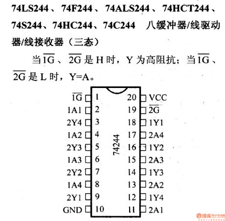
When 1G, 2G are H, Y is in high resistance; when 1G, 2G are L, Y=A.
(View)
View full Circuit Diagram | Comments | Reading(3500)
ELECTRONIC_CROWBAR_FOR_AC_OR_DC_LINES
Published:2009/6/28 22:29:00 Author:May


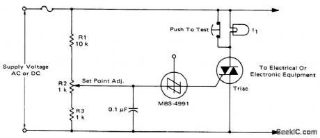
For positive protection ofelectrical or electronic equipment, use this against excessive supply voltage. Due to improper switching, wiring, short circuits, or failure of reg-ulators, an electronic crowbar circuit can quickly place a short circuit across the power lines, thereby dropping the voltage across the protected device to near zero and blowing a fuse. The triac and SBS are both bilateral devices, the circuit is equally useful on ac or dc supply lines. With the values shown for R1, R2, and R3, the crowbar operating point can be adjusted over the range of 60 to 120 volts dc or 42 to 84 volts ac. The resistor values can be changed to cover a different range of supply voltages. The voltage rating of the triac must be greater than the highest operating point as set by R2. I1 is a low power incandescent lamp with a voltage rating equal to the supply voltage. It may be used to check the set point and operation of the unit by opening the test switch and adjusting the input or set point to fire the SBS. An alarm unit such as the Mallory Sonalert may be connected across the fuse to provide an audible indication of crowbar action.(This circuit may not act on short, infrequent power line transients). (View)
View full Circuit Diagram | Comments | Reading(1689)
IC_VCO_with_split_supply_and_fixed_frequency
Published:2009/7/25 4:07:00 Author:Jessie
This circuit is similar to that of Fig. 5-36, except that a split supply is used, and the output is at a fixed frequency, determined by R3 and C as shown by the equations. (View)
View full Circuit Diagram | Comments | Reading(602)
74 Series digital circuit of 74LS241,74F241 eight inverting buffer/line driver/ line receiver(three-state)
Published:2011/8/1 1:06:00 Author:Lucas | Keyword: 74 Series , digital circuit , eight inverting buffer, line driver , line receiver, three-state
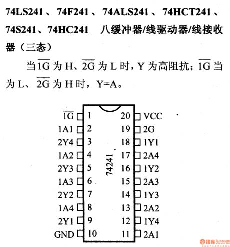
When 1G is H, 2G is L, Y is in high resistance; when 1G is L, and 2G is H, Y=A.
(View)
View full Circuit Diagram | Comments | Reading(1044)
BATTERY_MONITOR
Published:2009/6/28 22:27:00 Author:May
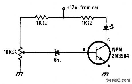
Basic circuit energizes LED when battery voltage drops to level set by 10K pot. Any number of additional circuits can be added, for reading battery voltage in 1-V steps oreven steps assmall as 0.1 V. Circuitsup-plements idiot light that replaces ammeter in most modern cars. LED type is not criticaL-J. Sandier, 9 Pro jects under $9, Modem Electron-ics, Sept, 1978, p 35-39. (View)
View full Circuit Diagram | Comments | Reading(2442)
The Schmidt trigger circuit
Published:2011/7/23 22:38:00 Author:Seven | Keyword: Schmidt trigger
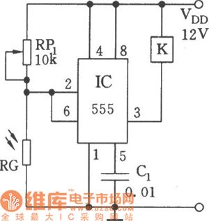
See as the figure, the circuit is based on 555, and 555 with LDR RG and RP1 composes the circuit. The resistance of RG changes with the light, by using the resetting and offsetting feature of the 2 comparators in 555, the Schmidt trigger is formed. When the light is strong, RG is in a low resistance, 2-pin is in low LEV(<1/3 VDD), 555 is offset, K is still; when the light is weak, RG is in a high resistance, 6-pin LEV is higher than 2/3VDD threshold LEV, 555 is reset, K is pulling in. (View)
View full Circuit Diagram | Comments | Reading(1095)
_5_V_from___5_Vor_four_to_eight_cells
Published:2009/7/25 4:06:00 Author:Jessie
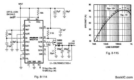

Figure 8-114 shows a MAX714 PWM regulator connected to provide-5 V from a four- to eight-cell battery (or a fixed +5-V Source). Figure 8-115 shows theefficiency curves. The input voltage range is 4 V to 15 V, with a quiescent current of 3 mA (VIN =5 V), a maximum load current of 1 A(VIN =4.75 V), and 1.25 A (VIN=12V), and a shutdown current of 30 μA. MAXIM BATTERY MANAGEMENT CIRCUIT COLLECTION. 1994, P. 56.
(View)
View full Circuit Diagram | Comments | Reading(672)
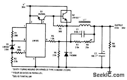
60_A_VARIABLE_OUTPUT_SWITCHING_REGULATOR
Published:2009/6/28 22:26:00 Author:May
View full Circuit Diagram | Comments | Reading(872)
COLD_WEATHER_IGNITION
Published:2009/6/28 22:25:00 Author:May
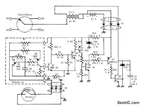
Multispark electronic ignition improves cold-weather starting ability of engines in arctic environment by providing more than one spark per combustion cycle. Circuit uses UJT triangle-wave generator Q1, emitter-follower isolator Q2, wave-shaping Schmitt trigger Q3-Q4, three stages of squarewave amplification Q5-Q7, and output switching circuit Q8 all operating from 12-V negative-ground supply. 6.2-V zener provides regulated voltage for UJT and Schmitt trigger. Initial 20,-000- to 40,000-V ignition spark produced by opening of breaker points is followed by continuous series of sparks at rate of about 200 per second as long as points stay open.-D. E. Stinchcomb, Multi-Spark Electronic Ignition for Engine Stating in Arctic Environment, Proceedings of the IEEE 1975 Region Six Conference, May 1975, p 224-225. (View)
View full Circuit Diagram | Comments | Reading(1234)
IC_VCO_voltrtge_controlled_oscillcltor_with_single_supply
Published:2009/7/25 4:05:00 Author:Jessie
This circuit is similar to that of Fig. 5-36, except that a single supply is used. (View)
View full Circuit Diagram | Comments | Reading(641)
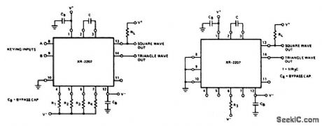
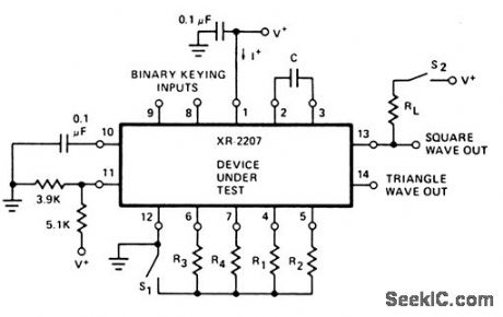
IC_VCO_voltrtge_controlled_oscillator_with_split_supply
Published:2009/7/25 4:05:00 Author:Jessie
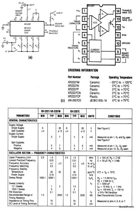
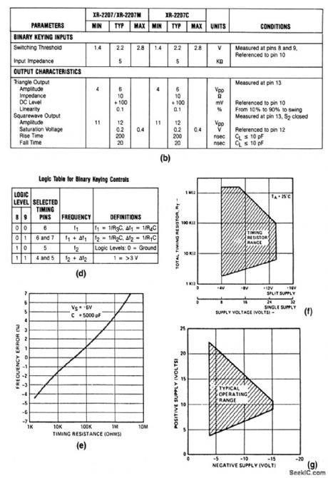
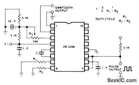
This circuit uses an XR-2207 to provide simultaneous triangle and square outputs (with binary keying if desired) over a frequency range of 0.01 Hz to 1 MHz, with a typical drift of 10 ppm/°C. The output can be linearly swept over a 1000:1 range with an external control voltage. Both the triangle and square output duty cycle can be varied from 0.1% to 99.9%. Electrical characteristics and functional circuits of the XR-2207 are shown in Figs. 5-36B and 5-36C, respectively. Operating frequency is set by capacitor C between pins 2 and 3, and timing resistors at pins 4-7. See Conditions in Fig. 5-36B. (View)
View full Circuit Diagram | Comments | Reading(699)
MULTIPLE_OUTPUT_SWITCHING_REGULATOR_FOR_USE_WITH_MPUs
Published:2009/6/28 22:25:00 Author:May
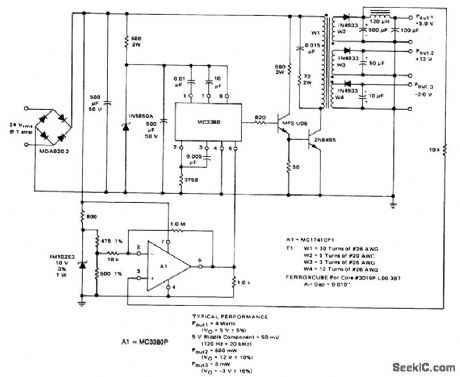
View full Circuit Diagram | Comments | Reading(713)
4 types of basic circuits of the single steady trigger composed of 555
Published:2011/7/24 1:43:00 Author:Seven | Keyword: single steady trigger, basic circuits
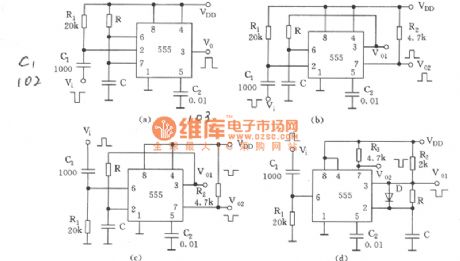
In Figure (a) is the typical single steady circuit. When an external pulse is added on the 2-pin of 555 after being past the C1 and R1 differential circuit, the forward pulse makes 555 offset, 3-pin is outputting a contemporary stable pulse width td=1.1RC. Figure b is like figure a, but it has 2 output terminals. C discharges the internal current of 555 through R, the recovering time is longer than that of Figure a. In figure c, the 2-pin and 6-pin of the circuit are different from figure a and figure b, the external trigger should be a forward pulse.
(View)
View full Circuit Diagram | Comments | Reading(700)
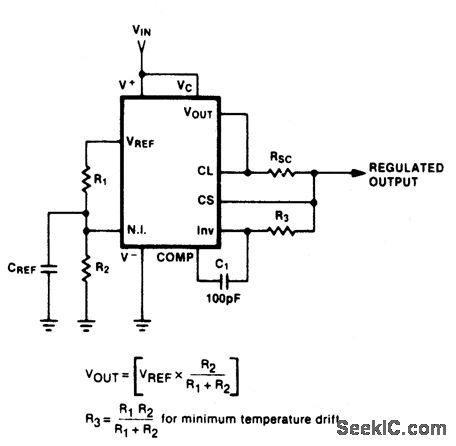
1ADJUSTABLE_OUTPUT_REGULATOR
Published:2009/6/28 22:23:00 Author:May
View full Circuit Diagram | Comments | Reading(620)
_5_V_from_a_negcttive_input_voltage
Published:2009/7/25 4:03:00 Author:Jessie
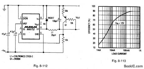
Figure 8-112 shows a MAX752 step-up regulator connected to provide a +5-V output from a 6-V to -15-V input (six- to eight-cell battery). Quiescent current with a VIN of -6 V is 1.5 mA, and maximum load current with a VIN of -6 V is 500 mA. Figure 8-113 shows the efficiency curves. The circuit works only in situations where the negative battery terminal need not be tied to ground (in systems that do not require multiple-output voltages taken from the battery). MAXIM BATTERY MANAGEMENT CIRCUIT COLLECTION, 1994, P. 3 (View)
View full Circuit Diagram | Comments | Reading(590)
SIMPLE_SPLIT_POWER_SUPPLY
Published:2009/6/28 22:22:00 Author:May
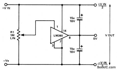
This circuit utilizes the quasicomplementary output stage ofthe popular LM380 audio power IC. The device is internally biased so that with no input the output is held midway between the supply rails. R1, which should be initially set to mid-travel, is used to nullify any inbalance in the output.Regulation of Vout depends upon the circuit feeding the LM380, but positive and negative outputs will track accurately irrespective of input regulation and unbalanced loads. The free-air dissipation is a little over 1 watt, and so extra cooling may be required. The device is fully protected and will go into thermal shutdown if its rated dissipation is exceeded. Current limiting occurs if the output current exceeds 1.3 A. The input voltage should not exceed 20 V. (View)
View full Circuit Diagram | Comments | Reading(835)
LOW_VOLTAGE_REGULATOR(VSUBout_SUB=2_TO_7_V)
Published:2009/6/28 22:21:00 Author:May
View full Circuit Diagram | Comments | Reading(621)
IC_function_generator_connected_for_pulse_and_ramp_outputs
Published:2009/7/25 4:01:00 Author:Jessie
This circuit is similar to that of Fig. 5-31, except that the XR-2206 is connected for pulse and ramp outputs. In this mode, the FSK keying terminal (pin 9) is shorted to the square output (pin 11), and the IC automatically frequency-shift keys itself between two separate frequencies during the positive-going and negative-going output waveforms. The pulse width and duty cycle can be adjusted from 1% to 99% by selection of R1 and R2, using the equations. The values of R1 and R2 should be in the range of 1 kΩ to 2 MΩ. (View)
View full Circuit Diagram | Comments | Reading(2528)
Q_MULTIPLIER_FOR_LOOP
Published:2009/6/28 22:20:00 Author:May
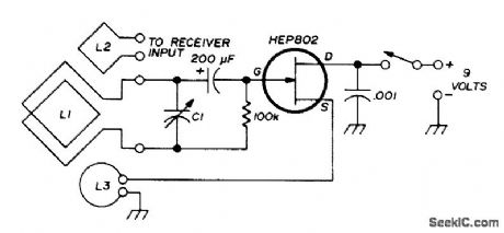
Improves performance of loop antenna on 40,80, and 160 meters. Feedback control is obtained with adjustable single-turn loop L3 coupled to L1, and receiver input is taken from L2. L3 is rotated within field.of L1 to adjust amount of regeneration, optimize circuit a, and make directional null more pronounced, Article gives loop con-struction details. Ground lower end of 100K ret sistorto provideground return for FET.-K, Cor-nell, Loop Antenna Receiving Aid, Ham Radio, May 1975, p 66-70. (View)
View full Circuit Diagram | Comments | Reading(2884)
IC_function_generator_connected_for_FSK_frequency_shift_keying
Published:2009/7/25 4:00:00 Author:Jessie
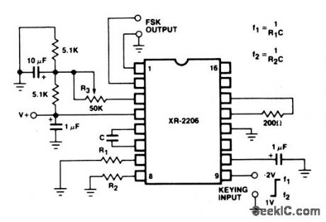
This circuit is similar to that of Fig. 5-31, except that the XR-2206 is connected for sine FSK outputs. Mark and space frequencies f1 and f2 are selected by the choice of R1, R2, and C, as shown by the equation. The output is phase-continuous during transitions. The keying signal is applied at pin 9. The circuit can be converted to split-supply operation by replacing ground with V-.R3 sets the FSK output amplitude. (View)
View full Circuit Diagram | Comments | Reading(2335)
| Pages:1271/2234 At 2012611262126312641265126612671268126912701271127212731274127512761277127812791280Under 20 |
Circuit Categories
power supply circuit
Amplifier Circuit
Basic Circuit
LED and Light Circuit
Sensor Circuit
Signal Processing
Electrical Equipment Circuit
Control Circuit
Remote Control Circuit
A/D-D/A Converter Circuit
Audio Circuit
Measuring and Test Circuit
Communication Circuit
Computer-Related Circuit
555 Circuit
Automotive Circuit
Repairing Circuit