
Circuit Diagram
Index 1278
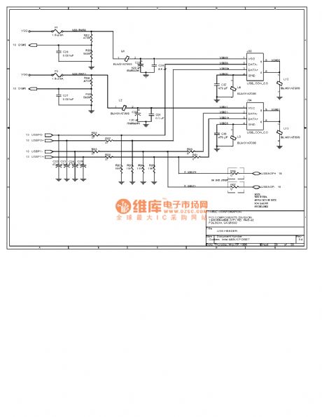
Computer motherboard circuit diagram 440LX2_21
Published:2011/7/31 22:00:00 Author:Ecco | Keyword: Computer motherboard
View full Circuit Diagram | Comments | Reading(590)
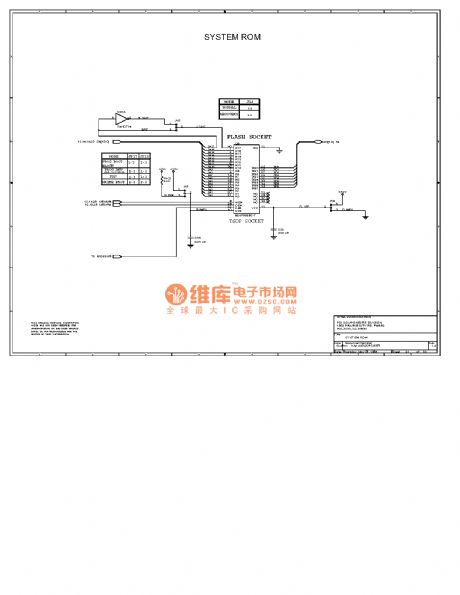
Computer motherboard circuit diagram 440LX2_20
Published:2011/7/31 21:59:00 Author:Ecco | Keyword: Computer motherboard
View full Circuit Diagram | Comments | Reading(559)
CMOS 555 equivalent function box circuit diagram
Published:2011/7/31 22:08:00 Author:Ecco | Keyword: CMOS, 555 , equivalent function box
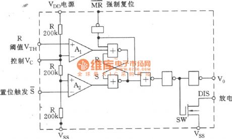
View full Circuit Diagram | Comments | Reading(1171)
Color ring display circuit diagram of foreign capacitor
Published:2011/7/31 22:10:00 Author:Ecco | Keyword: Color ring display, foreign capacitor
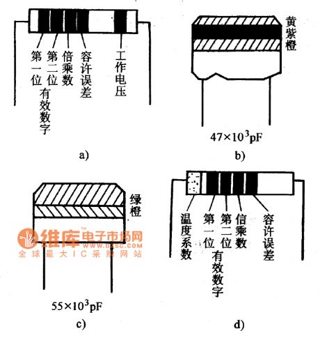
View full Circuit Diagram | Comments | Reading(529)
A digital power amplifier circuit diagram
Published:2011/7/31 22:11:00 Author:Ecco | Keyword: digital power amplifier
View full Circuit Diagram | Comments | Reading(661)
5.1ch amplifier circuit diagram
Published:2011/7/31 22:10:00 Author:Ecco | Keyword: 5.1ch amplifier
View full Circuit Diagram | Comments | Reading(8261)
LOW_RIPPLE_POWER_SUPPLY
Published:2009/6/28 21:45:00 Author:Jessie
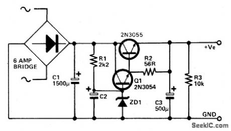
This circuit may be used where a high current is required with a low ripple voltage (such as in a high powered class AB amplifier when high quality reproduction is necessary). Q1, Q2, and R2 may be regarded as a power darlington transistor. ZD1 and R1 provide a reference voltage at the base of Q1. ZD1 should be chosen thus: ZD1 = Vout-1.2. C2 can be chosen for the degree of smoothness as its value is effectively multiplied by the combined gains of Q1/Q2, if 100 μF is chosen for C2, assuming minimum hfe for Q1 and Q2, C = 100 x 15(Q1) x 25(Q2) = 37,000 μF. (View)
View full Circuit Diagram | Comments | Reading(1883)
15_V/1_A_REGULATOR_WITH_REMOTE_SENSE_
Published:2009/6/28 21:43:00 Author:Jessie
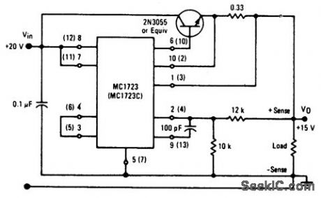
View full Circuit Diagram | Comments | Reading(1928)
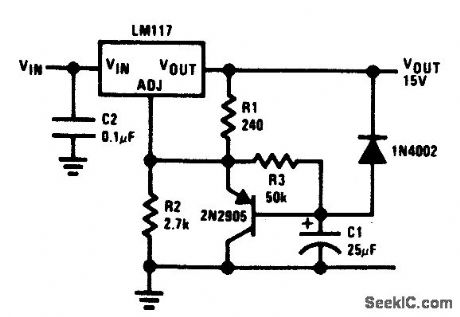
SLOW_TURN_ON_15_V_REGULATOR_
Published:2009/6/28 21:43:00 Author:Jessie
View full Circuit Diagram | Comments | Reading(818)
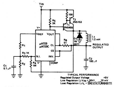
5_V/1_A_SWITCHING_REGULATOR_
Published:2009/6/28 21:42:00 Author:Jessie
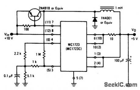
View full Circuit Diagram | Comments | Reading(651)
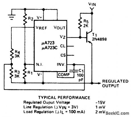
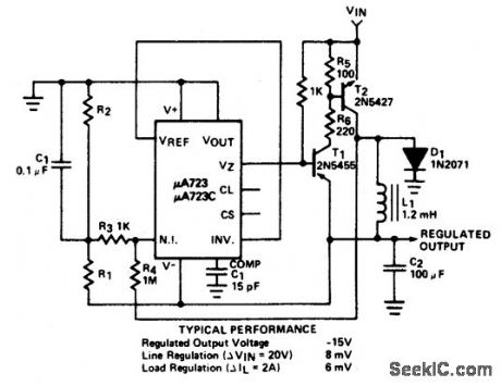
-15_V_NEGATIVE_REGULATOR_
Published:2009/6/28 21:41:00 Author:Jessie
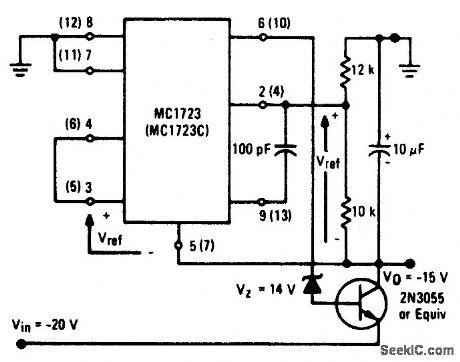
View full Circuit Diagram | Comments | Reading(804)
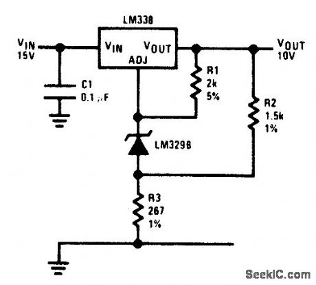
HIGH_STABILITY_10_V_REGULATOR_
Published:2009/6/28 21:41:00 Author:Jessie
View full Circuit Diagram | Comments | Reading(596)
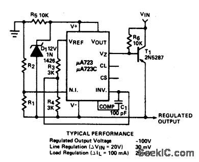
NEGATIVE_VOLTAGE_REGULATOR__
Published:2009/6/28 21:40:00 Author:Jessie
View full Circuit Diagram | Comments | Reading(645)
LED_BAR_PEAK_PROGRAM_METER_DISPLAY_FOR_AUDIO
Published:2009/6/28 21:39:00 Author:Jessie

Circuit NotesA bar column of LEDs is arranged so that as the audio signal level increases, more LEDs in the column light up. The LEDs are arranged vertically in 6 dB steps. A fast response time and a one second decay time give an accurate response to transients and a low flicker decay characteristic. On each of the op amps inverting inputs is a dc reference voltage, which increases in 6 dB steps. All noninverting inputs are tied together and connected to the positive peak envelope ofthe audio signal.hus, as this envelope exceeds a particular voltage reference, the op amp output goes high and the LED lights up. Also, all the LEDs below this are illuminated. (View)
View full Circuit Diagram | Comments | Reading(810)
1NEGATIVE_FLOATING_REGULATOR
Published:2009/6/28 21:38:00 Author:Jessie
View full Circuit Diagram | Comments | Reading(529)
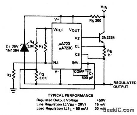
POSITIVE_SWITCHING_REGULATOR
Published:2009/6/28 21:37:00 Author:Jessie
View full Circuit Diagram | Comments | Reading(524)
NEGATIVE_FLOATING_REGULATOR
Published:2009/6/28 21:36:00 Author:Jessie
View full Circuit Diagram | Comments | Reading(598)
NEGATIVE_SWITCHING_REGULATOR
Published:2009/6/28 21:36:00 Author:Jessie
View full Circuit Diagram | Comments | Reading(602)
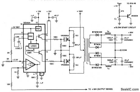
±50_V_PUSH_PULL_SWITCHED_MODE_CONVERTER
Published:2009/6/28 21:21:00 Author:May
View full Circuit Diagram | Comments | Reading(2449)
HEADLIGHT_REMINDER
Published:2009/6/28 21:21:00 Author:May
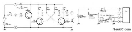
Uses basic oscillator consisting ofQ2 and Q3 arranged as collectorcoupled astable MVBR. Power is taken from collector of Q1 which acts as switch for Q2 and Q3. With S1 closed and S2 open, oscillator operates. Closing S2 saturatesQ1 and stops oscillator. When used as headlight reminder for negativeground car, B1 is omitted and power for oscillator is taken from dashboard panel lights since they come on simultaneously with either parking lights or headlights. If ignition key is turned on, al saturates and disables Q2-Q3. With ig-nition off but lights on, Q1 is cut off and oscillator receives power. Audio output may be connected directly to high side of voice coil of car radio loudspeaker without affecting operation of radio. Almost any NPN transistors can be used. Changing values of R4 and R5 changesfre-quency of reminder tone.-H. F. Batie, Versatile Audio Oscillator, Ham Radio, Jan. 1976, p 72-74. (View)
View full Circuit Diagram | Comments | Reading(860)
| Pages:1278/2234 At 2012611262126312641265126612671268126912701271127212731274127512761277127812791280Under 20 |
Circuit Categories
power supply circuit
Amplifier Circuit
Basic Circuit
LED and Light Circuit
Sensor Circuit
Signal Processing
Electrical Equipment Circuit
Control Circuit
Remote Control Circuit
A/D-D/A Converter Circuit
Audio Circuit
Measuring and Test Circuit
Communication Circuit
Computer-Related Circuit
555 Circuit
Automotive Circuit
Repairing Circuit