
Circuit Diagram
Index 1276
DAC_with_bipolar_output_from_a_fixed_reference
Published:2009/7/25 5:33:00 Author:Jessie
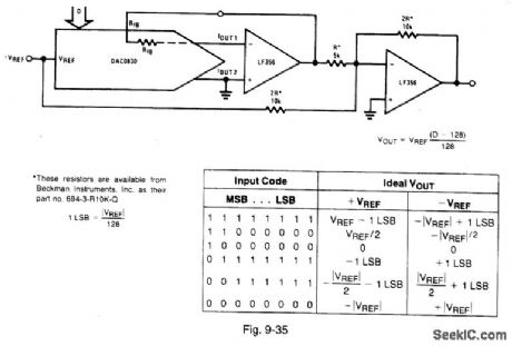
Figure 9-35 shows a DAC0830 connected to provide a bipolar output from a fixed reference voltage. This connection is made with a second op amp in the analog-output circuit. In effect, the circuit gives sign significance to the MSB of the digital-input word, allowing four-quadrant multiplication of the reference voltage. The polarity of the reference can still be reversed (or can be an ac signal) to realize full four-quadrant multiplication. NATIONAL SEMICONDUCTOR, APPLICATION Now 271, 1994 P. 666.
(View)
View full Circuit Diagram | Comments | Reading(1300)
DAC_connected_for_single_supply_operation
Published:2009/7/25 5:31:00 Author:Jessie
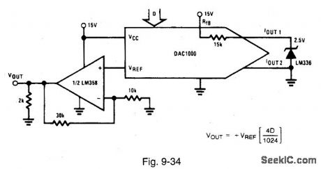
Figure 9-34 shows a DAC1000 connected for single-supply operation. The R-2R ladder can be operated as a voltage-switching network to prevent the output-voltage inversion that is so common in the current-switching mode. In this circuit, the reference voltage is applied to the IOUT 1 terminal and is attenuated by the R-2R ladder in proportion to the applied code. The voltage is then output to the VREF terminal with no phase inversion. To ensure linear operation in single-supply modes, the applied voltage must be kept less than 3 V for 10-bit DACs, or less than 5 V for 8-bit DACs. The supply voltage to the DAC must be at least 10 V more positive than the reference voltage to ensure that the CMOS ladder switches have enough voltage Qverdrive to fully turn on. An external op amp can be added to provide gain to the DAC output voltage for a wide overall output span. This circuit provides generally good linearity for 8-bit and 8-bit DACs, but can have a problem with 12-bit DACs (because of the very low reference required). If 12-bit operation is desired, use a DAC specifically designed for single-supply operation. NATIONAL SEMICONDUCTOR, APPLICATION NOTE 271, 1994, P. 666. (View)
View full Circuit Diagram | Comments | Reading(862)
DAC_with_level_shifted_output
Published:2009/7/25 5:30:00 Author:Jessie
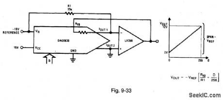
Figure 9-33 shows a DAC0830 operated with the output level shifted. The shift is made by summing a fixed current to the DAC current-output terminal, offsetting the output voltage to the op amp. The applied reference voltage then serves as the output-span controller and is added (in fractions) to the output as a function of the applied digital code. NATIONAL SEMICONDUCTOR, APPLICATION NOTE 271, 1994, P. 665. (View)
View full Circuit Diagram | Comments | Reading(1108)
Digital_potentiometer_with_composite_amplifier
Published:2009/7/25 5:26:00 Author:Jessie
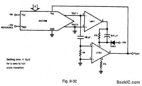
Figure 9-32 shows a DAC1208 connected as a digital pot with improved characteristics (over those of the Fig. 9-31 circuit). The Fig. 9-32 circuit combines the excellent dc input characteristics of the classic LM11 with the fast response of a LF351 (a combination bipolar device). NANONAL SEMICONDUCTOR, APPLICATION NOTE 271, 1994, P. 665.
(View)
View full Circuit Diagram | Comments | Reading(806)
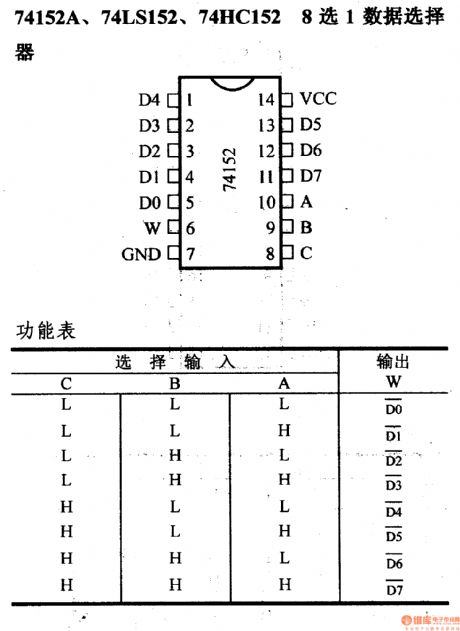
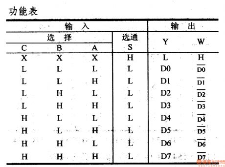
74 Series digital circuit of 74152A, 74LS152 8-to-1 data selector
Published:2011/7/25 3:51:00 Author:Lucas | Keyword: 74 Series , digital circuit, 8-to-1 data selector
View full Circuit Diagram | Comments | Reading(1214)
Digital_potentiometer
Published:2009/7/25 5:25:00 Author:Jessie
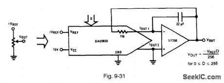
Figure 9-31 shows a DAC0830 connected as a digital potentiometer (pot). The applied digital-input word multiplies the applied reference voltage. The resultant output voltage is the product of this multiplication, normalized to the resolution of the DAC. The op amp converts the DAC output current to a voltage through the 15-kΩ feedback resistor within the DAC. To preserve output linearity, the two current-output pins must be as close to 0 V as possible. Thus, the input-offset voltage of the op amp must be nulled. The amount of linearity-error degradation is about VOS + VREF When the digital pot is used to attenuate ac signals (in audio applications, for example), the DAC linearity over the full range of the applied reference voltage (even if it passes through zero) is good enough to distort a 10-V sine wave by only 0.004%. NATIONAL SEMICONDUCTOR, APPLICATION NOTE 271, 1994, P. 665.
(View)
View full Circuit Diagram | Comments | Reading(903)
Sine_wave_generator_with_digital_control
Published:2009/7/25 5:23:00 Author:Jessie
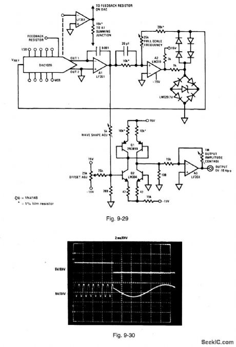
Figure 9-29 shows a DAC1020 connected to provide a variable-frequency, sine-wave generator. This circuit is capable of producing signals at frequencies up to 30 kHz under digital control. The linearity of the output frequency to the digital-code input is within 0.1% for each of the 1024 discrete output frequencies. To adjust the circuit, set all DAC digital inputs high and trim the 25-kΩ pot for a 30-kHz output (using a frequency counter). Then connect a distortion analyzer to the circuit output and adjust the 5-kΩ and 75-kΩ pots for minimum distortion. Finally, set the 1-MΩ output control for the desired output. The circuit provides rapid switching of the output frequency, as shown in Fig. 9-30. Notice that the output frequency shifts immediately (actually with no undesired delay) by more than an order of magnitude in response to digital commands (top line of Fig. 9-30). If operation over temperature is required, the absolute change in resistance in the DAC internal ladder might cause unacceptable errors. This can be corrected by reversing the A2 inputs and inserting an amplifier (dashed lines in Fig. 9-29) between the DAC and A1. Because this amplifier uses the DAC internal feedback resistor (Fig. 9-28), the temperature error in the ladder is cancelled. This results in more stable operation. NATIONAL SEMICONDUCTOR, APPLICATION NOTE 269, 1994, P. 660. (View)
View full Circuit Diagram | Comments | Reading(1053)
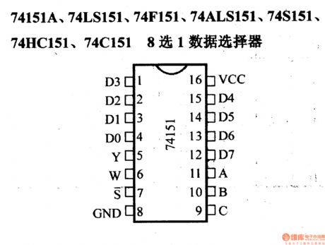
74 Series digital circuit of 74151A, 74LS151 8-to-1 data selector
Published:2011/7/25 3:52:00 Author:Lucas | Keyword: 74 Series, digital circuit , 8-to-1 data selector
View full Circuit Diagram | Comments | Reading(4310)
Multiplying_DACs
Published:2009/7/25 5:18:00 Author:Jessie
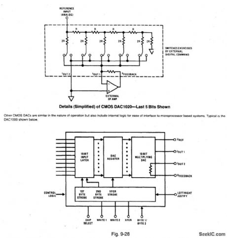
Figure 9-28 shows the internal functions of a multiplying DAC. Because Such four-quadrant DACs allow a digital word to operate on an analog input, or vice versa, the output can represent a sophisticated function. CMOS multiplying DACs allow true bipolar analog signals to be applied to the reference input. This feature makes such DACs useful in many applications that are not generally considered data converters. NATIONAL SEMICONDUCTOR, APPLICATION NOTE 269, 1994, P. 659. (View)
View full Circuit Diagram | Comments | Reading(673)
Partially_decoded_6800_interface
Published:2009/7/25 5:17:00 Author:Jessie
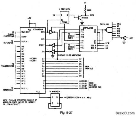
Figure 9-27 shows the ADC0816/17 connected to form a partially decoded 6800 interface. This interface has more I/O-port strobes than the circuit of Fig. 9-26. A NAND gate and inverter are used to decode the addresses, VMA, and phase-2 clocki The I/O addresses are located at 11110XXXXXAABBBB (binary); where X = don't care; A = 00 (binary) for ALE write or IREQ reset/EOC read and A = 01 for START write or data read; and B channel-select address, if A, B, C, and D are connected to the address bus and ALE is accessed. A dual2-4 line decoder is used to generate these strobes. Inverters are used to create the correct logic levels. The 6800 supports only a wired-OR interrupt structure. In a multi-interrupt environment, only one interrupt is received and the interrupt-handler routine must determine which device has cause the interrupt and must service that device.To do this, the EOC is brought out to the data bus so that EOC can be checked by the CPU. NATIoNAL SEMICONDUCTOR, APPLICATION NOTE 258, 1994, P. 610. (View)
View full Circuit Diagram | Comments | Reading(692)
Simple_6800_interface
Published:2009/7/25 5:15:00 Author:Jessie
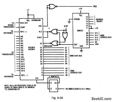
Figure 9-26 shows the ADC0816/17 connected for a simple-or minimum 6800 interface. This circuit uses a DM8131 comparator to partically decode the A12, A13, A14, and A15 address lines with the phase-2 clock and VMA (valid memory address). This provides an address-decode pulse for the two NOT gates, which in turn generate the START/ALE pulse and the output-enable OE signal. Ihe design locates the ADC in one 4-kb or block. EOC is tied to IREQ interrupt through an inverter, and is usable only in single-interrupt systems because the 6800 has no way of resetting the interrupt (except by starting a new conversion). Because EOC is directly ties to the interrupt input, the controlling software must not re-enable interrupts until eight converter clock periods after the start pulse, when EOC is low. NATIONAL SEMICONDUCTOR, APPLICATION NOTE 258, 1994, P. 610.
(View)
View full Circuit Diagram | Comments | Reading(1177)
Minimum_NAC800_interface
Published:2009/7/25 5:13:00 Author:Jessie
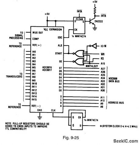
Figure 9-25 shows the ADC0816/17 connected to form a simple or minimum NAC800 interface. This circuit uses NOR gates (similar to that of Fig. 9-20), but with different control signals. When EOC goes high, the flip-flop is set and INTR goes low. When the NSC800 acknowledges the interrupt by lowering INTA, the flip-flop resets. If more than one interrupt can occur simultaneously, either INTA should be gated with EOC, or a signal other than INTA must be used. This is required because the NSC800 can detect another interrupt and clear the ADC interrupt before the ADC signal is detected. NATIONAL SEMICONDUCTOR, APPLICATION NOTE 258, 1994, P. 609. (View)
View full Circuit Diagram | Comments | Reading(668)
Partially_decoded_NSC800_interface
Published:2009/7/25 5:12:00 Author:Jessie
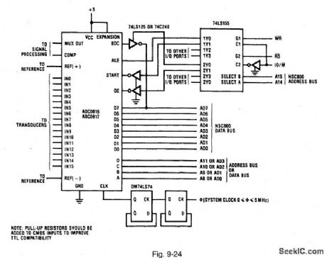
Figure 9-24 shows the ADC0816/17 connected to form a partially coded NSC800 interface. This interface is quite similar to that for the 8080-even though the timing is very different. The NSC800 multiplexes the lower 8 address bits on the data bus at the beginning of each cycle. When accessing memory, A0 through A7 must be latched out at the beginning of a read or write cyde. For I/O accessing, the NSC800 duplicates the 8-bit I/O addresses on A8 through A15 address lines. Latches are not necessary because these lines are not multiplexed. The I/O read and write strobes are taken from RD (read) and WR (write) lines and the IO/M signal. A dual 2-4 line decoder decodes A15. A14 is enabled by the read-write strobes. Tristate inverters are used to implement a decoding stmitar to that of Fig. 9-21. Double pulsing is not required because START and ALE are accessed separately. NATIONAL SEMICONDUCTOR, APPLICATION NOTE 258, 1994, P. 608.
(View)
View full Circuit Diagram | Comments | Reading(890)
EXCLAMATION_POINT_DISPLAY
Published:2009/6/28 21:34:00 Author:May
View full Circuit Diagram | Comments | Reading(706)
74 Series digital circuit of 74148,74LS148 8-3 line priority encoder
Published:2011/7/25 3:54:00 Author:Lucas | Keyword: 74 Series , digital circuit , 8-3 , line priority encoder
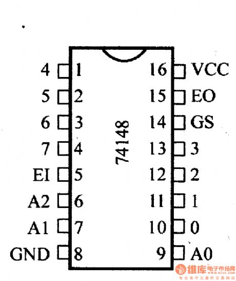
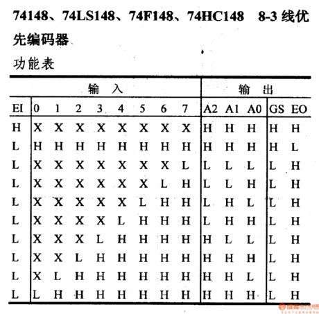
View full Circuit Diagram | Comments | Reading(10118)
MOBILE_VOLTAGE_REGULATOR
Published:2009/6/28 21:34:00 Author:May
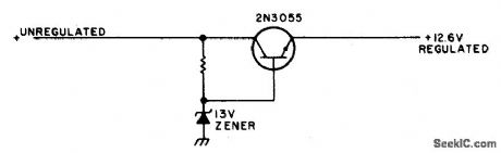
This simple mobile voltage regulator circuit may save your two meter or CB transceiver if the voltage regulator fails. The 2N3055 should be heat sinked if current drawn by the rig is in excess of 2 A on transmit. This circuit will do little under normal operating conditions, but could save expensive equipment if the vehicle's electrical system loses regulation. (View)
View full Circuit Diagram | Comments | Reading(1394)
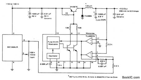
50_V/60_A_25_kHz_SWITCHING_REGULATOR_WITH_SEPARATE_ULTRA_STABLE_REFERENCE
Published:2009/6/28 21:31:00 Author:May
View full Circuit Diagram | Comments | Reading(807)
74 Series digital circuit of 74147,74LS147 decimal 4 line BCD priority encoder
Published:2011/7/25 3:57:00 Author:Lucas | Keyword: 74 Series , digital circuit , decimal 4 line , BCD priority encoder
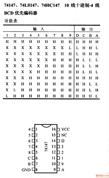
View full Circuit Diagram | Comments | Reading(4755)
HEADLIGHTS_ON_ALARM
Published:2009/6/28 21:31:00 Author:May
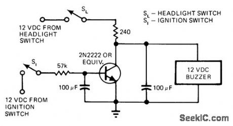
Designed for cars in which headlight switch is nongrounding type, providing 12 V when dosed. When both light and ignition switches are closed, transistor is saturated and there is no voltage drop across it to drive buzzer. If ignition switch is open while lights are on, transistor bias is removed so transistor is effectively open and full 12 V is applied to buzzer through 240-ohm resistor until lights are turned off.-R. E. Hartzell, Jr., Detector Warns You When Headlights Are Left On, EDN Magazine, Nov. 20, 1975, p 160. (View)
View full Circuit Diagram | Comments | Reading(903)
74 Series digital circuit of 74145,74LS145 BCD decimal decoder / driver (OC)
Published:2011/7/25 4:01:00 Author:Lucas | Keyword: 74 Series , digital circuit , BCD decimal decoder , BCD decimal driver , OC
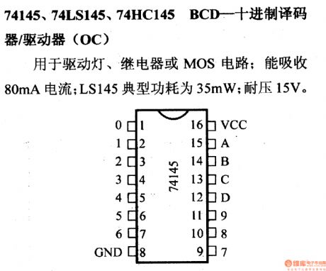
It is used to drive lamp, relay or MOS circuit; it can absorb 80mA current; the typical power consumption of LS145 is 35mW; withstand voltage is 15V.
(View)
View full Circuit Diagram | Comments | Reading(2538)
| Pages:1276/2234 At 2012611262126312641265126612671268126912701271127212731274127512761277127812791280Under 20 |
Circuit Categories
power supply circuit
Amplifier Circuit
Basic Circuit
LED and Light Circuit
Sensor Circuit
Signal Processing
Electrical Equipment Circuit
Control Circuit
Remote Control Circuit
A/D-D/A Converter Circuit
Audio Circuit
Measuring and Test Circuit
Communication Circuit
Computer-Related Circuit
555 Circuit
Automotive Circuit
Repairing Circuit