
Circuit Diagram
Index 1264
LINE_DRIVER
Published:2009/6/28 23:23:00 Author:May
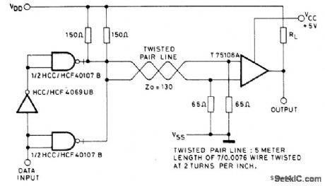
View full Circuit Diagram | Comments | Reading(0)
Inverting_buck_boost_converter
Published:2009/7/25 1:49:00 Author:Jessie

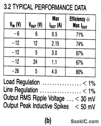
This circuit provides positive outputs for negative inputs at the same voltage, at a higher voltage, or at a lower voltage. Typical performance data and component source information are given in Figs. 4-36B and 4-36C, respectively. (View)
View full Circuit Diagram | Comments | Reading(855)
Inverting_step_down_converter_with_adjustable_output
Published:2009/7/25 1:47:00 Author:Jessie
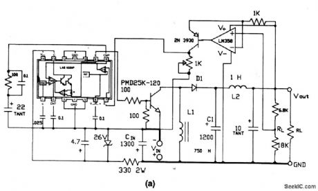
This circuit provides a +9 to +30 V output at 5 A from a -48-V input.Typical performance data and component source information are given in Figs.4-35B and 4-35C, respectively. (View)
View full Circuit Diagram | Comments | Reading(941)
50_OHM_DRIVER
Published:2009/6/28 23:21:00 Author:May
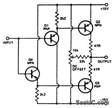
Circuit Notes
To buffer a test generator to the outside world requires an amplifier with sufficient bandwidth and power handling capability. The circuit is a very simple unity gain buffer. It has a fairly high input impedance, a 50 ohm output impedance, a wide bandwidth, and high slew rate. The circuit is simply two pairs of emitter ollowers. The base emitter voltages of Q1 and Q2 cancel out, and so do those of Q3 and Q4.The preset is used to zero out any small dc offsets due to mismatching in the transistors. (View)
View full Circuit Diagram | Comments | Reading(1728)
74 Series digital circuit of 74S412 multi-mode buffer latch (tristate)
Published:2011/7/25 3:25:00 Author:Lucas | Keyword: 74 Series , digital circuit , multi-mode buffer latch , tristate
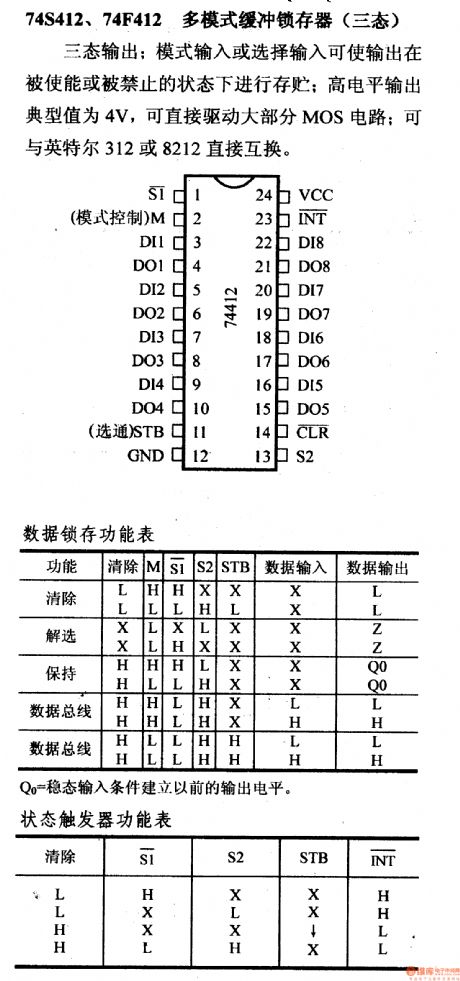
Three-state output; mode input or selecting input allows output to storage in the enabled or disabled state; the typical value of high output is 4V, which can directly drive most of the MOS circuit; it can exchange with Intel 312 or 8212 directly.
Q0 = the output level before establishing the steady-state input conditions.
(View)
View full Circuit Diagram | Comments | Reading(1098)
74 Series digital circuit of 74LS423, 74HC423 dual retriggerable monostable multivibrator (with clearing)
Published:2011/7/25 3:39:00 Author:Lucas | Keyword: 74 Series, digital circuit , dual retriggerable , monostable multivibrator , clearing
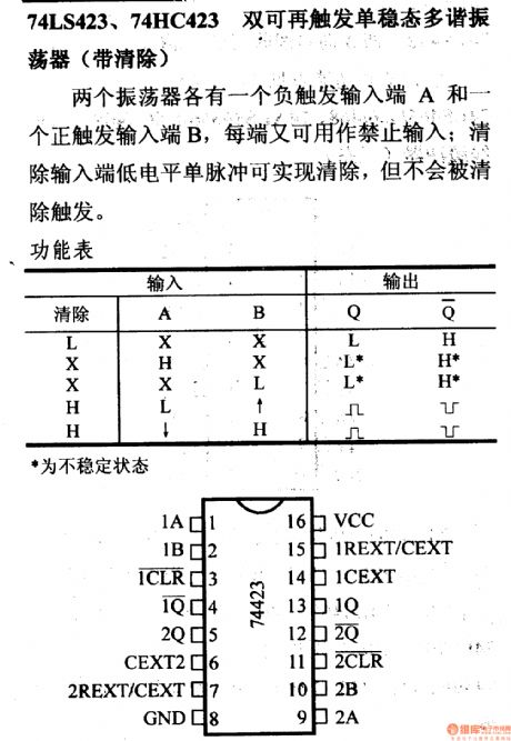
Two oscillators have a negative trigger input A and a positive trigger input B, but each end can be used to ban on the importation; when the clearing input end is in single-pulse low level, it is enable to clear, but will not be cleared trigger.
*is the unstable state.
(View)
View full Circuit Diagram | Comments | Reading(935)
35_W_BRIDGE_AMPLIFIER
Published:2009/6/28 23:21:00 Author:May
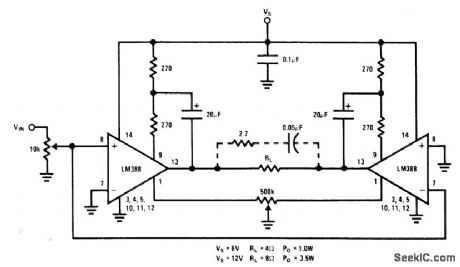
Bridge connection of National LM388 power opamps provides 3.5 W to 8-ohm loudspeaker when using 12-V supply. With 6-V supply and 4-ohm load, maximum power is 1 W. Coupling capacitors are not re quired since output DC levels are within several tenths of a volt of each other.- Audio Hand-book, National Semiconductor, Santa Clara, CA, 1977, p 4-37-4-41. (View)
View full Circuit Diagram | Comments | Reading(851)
HAMMER_DRIVER
Published:2009/6/28 23:21:00 Author:May
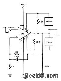
Signetics 540 power driver handles either push-pull or single-ended inductive loads such as relays, solenoids, motors, and electric hammers. In push-pull connection shown, load is driven in either positive, negative, or both arms of output. Either output can be selected by appropriate choice of input pulse polarity. Supply can be ±5 to ±25 V.- Signetics Analog Data Manual, Signetics, Sunnyvale, CA, 1977, p 764. (View)
View full Circuit Diagram | Comments | Reading(675)
30_W
Published:2009/6/28 23:20:00 Author:May
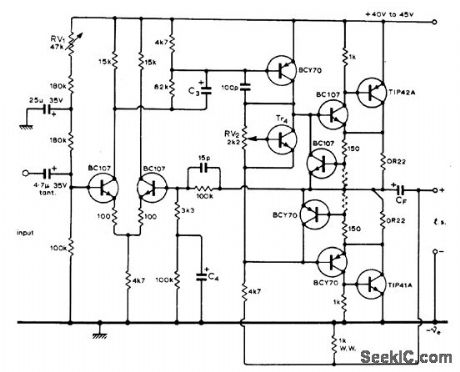
Designed for use with active filter crossover networks for three loudspeakers. For lowest-frequency channel, C3 is 150μF and C4 is 50μF. For middle channel, C3 and C4 are 25μF. For high-frequency channel, C3 and C4 are 10μF.Article includes circuit for active filter network.-D. C. Read, Active Filter Crossover Networks, Wireless World, Dec. 1973, p 574-576. (View)
View full Circuit Diagram | Comments | Reading(793)
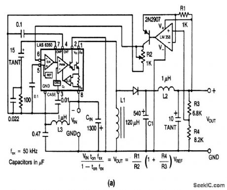
Step_down_voltage_regulator
Published:2009/7/25 3:03:00 Author:Jessie
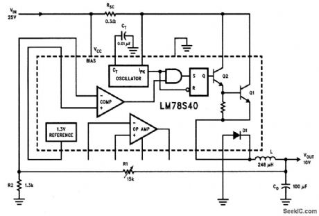
This circuit converts 25-V to an adjustable 10-V output at 500 mA, with less than 1% ripple. (View)
View full Circuit Diagram | Comments | Reading(1454)
CAPACITOR_SERVES_AS_IGNITION_BATTERY
Published:2009/6/28 23:17:00 Author:May
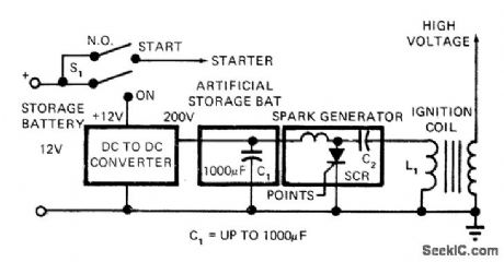
Developed for use with capacitor-discharge ignition systems to provide independent voltage sourcefor ignition when starting car in very cold weather. Before attempting to start car, S1 is set to ON position for energizing DC-to-DC converter for charging C1 with DC voltage between 200 and 400 V. Starter is now engaged. If voltage of storage battery drops as starter slowly turns engine over, C1 still represents equivalent of fully charged 12-V storage battery that is ca pable of driving ignition system for almost a minute.-W. Stalzer, Capacitor Provides Artificial Battery for Ignition Systems, EDN Mage-zine, Nov. 15, 1972, p 48. (View)
View full Circuit Diagram | Comments | Reading(1193)
Step_up_voltage_regulator_with_increased_voltage_current_ratings
Published:2009/7/25 2:46:00 Author:Jessie
This circuit is similar to that of Fig. 4-65, except that the input is 15 V, and the output is 70 V with less than 1% ripple. (View)
View full Circuit Diagram | Comments | Reading(1130)
Step_up_voltage_regulator
Published:2009/7/25 2:45:00 Author:Jessie
This circuit converts 5-V to an adjustable 15-V output at 150 mA, with less than 1 % ripple. (View)
View full Circuit Diagram | Comments | Reading(845)
Off_line_regulator_with_a_floating_intput
Published:2009/7/25 2:44:00 Author:Jessie
With this circuit, the input of the LT1070 switching regulator floats to a potential set by the output. (View)
View full Circuit Diagram | Comments | Reading(804)
Negative_to_positive_switched_capacitor_converter
Published:2009/7/25 2:43:00 Author:Jessie
This circuit is similar to that of Fig. 4-56, except that the input is negative and the output is positive. (View)
View full Circuit Diagram | Comments | Reading(748)
AUTO_TRAILER_INTERFACE_FOR_LIGHTS
Published:2009/6/28 23:13:00 Author:May
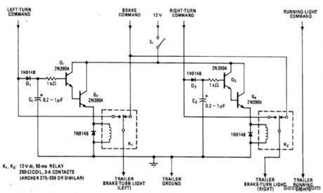


Low-cost transistors and two relays combine brake-light and tum-indicator signals on common bus to ensure that trailer lights respond to both commands. C1 and C2 charge to peak amplitude of tum signal, which flashes about 2 times per second. Values are selected to hold relay closed between flash intervals; if capacitance is too large, brake signal cannot immediately activate trailer lights after tum signal is canceled. Developed for new cars in which sep-arate turn and brake signals are required for safety.-M. E. Gilmore and C. W. Snipes, Dar-lington-Switched Relays Link Car and Trailer Signal Lights, Electronics, Aug. 18, 1971, p 116. (View)
View full Circuit Diagram | Comments | Reading(945)
Switched_capacitor_12_to_5_V_converter
Published:2009/7/25 2:42:00 Author:Jessie
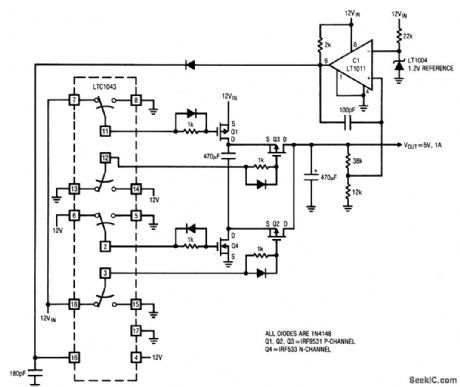
This circuit provides 5 V at 1 A from a 12-V input. (View)
View full Circuit Diagram | Comments | Reading(629)
The op-amp μA741 switch power supply circuit
Published:2011/7/24 3:53:00 Author:Seven | Keyword: op-amp, switch power supply
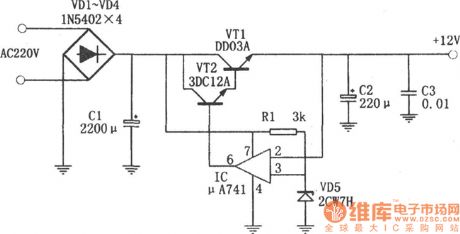
The power supply adopts with the op-amp μA741 as the comparator control element, 2 triodes as the regulating elements, the circuit is working the the open state. When the output voltage is 2mV lower than the Vref, i.e the 2-pin is 2mV lower than 3-pin(as the sensibility ofμA741 is 2mV), 6-pin of μA741 is outputting a high LEV, VT1 and VT2 are conducting, large current load and relevant capacitors of C2 and C3 compensate the power, soon the output voltage rises to 12V, i.e 2-pin and 3-pin of μA741 have the same LEV.
(View)
View full Circuit Diagram | Comments | Reading(1236)
Switched_capnacitor_5__to_±10_V_converter
Published:2009/7/25 2:41:00 Author:Jessie
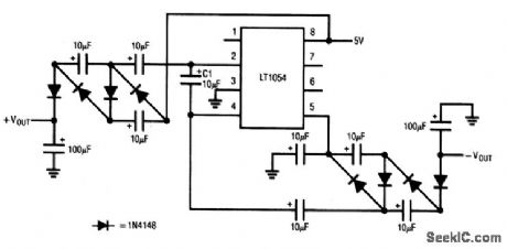
This circuit uses charge-pump principles to convert 5 V to ±10 V at 10 mA. At no load, the output is ± 13 V. (View)
View full Circuit Diagram | Comments | Reading(804)
Switched_capacitor_6__to_±7_V
Published:2009/7/25 2:40:00 Author:Jessie
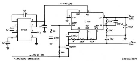
This circuit provides±7-V outputs at 20 mA from a 6-V input. (View)
View full Circuit Diagram | Comments | Reading(540)
| Pages:1264/2234 At 2012611262126312641265126612671268126912701271127212731274127512761277127812791280Under 20 |
Circuit Categories
power supply circuit
Amplifier Circuit
Basic Circuit
LED and Light Circuit
Sensor Circuit
Signal Processing
Electrical Equipment Circuit
Control Circuit
Remote Control Circuit
A/D-D/A Converter Circuit
Audio Circuit
Measuring and Test Circuit
Communication Circuit
Computer-Related Circuit
555 Circuit
Automotive Circuit
Repairing Circuit