
Circuit Diagram
Index 1275
Buffering_circuits
Published:2009/7/25 4:53:00 Author:Jessie
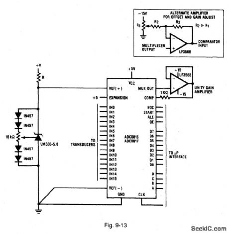

Figures 9-13 and 9-14 show two typical buffering circuits for the ADCs. Three basic ranges of input signal levels can occur when ADCs are interfaces to the real world. These are as follows: (1) signals that exceed VCC or go below ground; (2) signals with input ranges less than VCC and ground, but are different from the reference range; and (3) signals that have an input range equal to the reference range. Each of these situations requires different buffering. In the last case (in which the signals are equal to the reference), no buffering is usually required, unless the source impedance of the input signal is very high. In this case, a buffer can be added between the multiplexer output and comparator input (Fig. 9-13). An op amp with high input impedance and low output impedance reduces input leakage (when one views the configuration from the multiplexer). If the input signal is within the supply range, but different from the reference range (or when the reference cannot be manipulated to conform to the full input range), the unity-gain buffer of Fig. 9-13 can be replaced with another op amp (as shown in the inset of Fig. 9-13). This type of amplifier provides gain or offset control to produce a full-scale range equal to the reference. When the input range exceeds VCC or goes below ground, the input signals must be level-shifted before the input can go to the multiplexer. There is a limit to such level shifting when the input voltage range is with 5 V, but outside the 0.5-V supply range. In this case, the supply for the entire chip can be shifted to the input range, and the digital-output signals can be level-shifted to the system 5-V supply. A typical example of level-shifting and buffering is the situation in which the bipolar inputs range from -2.5 V to +2.5 V. If the ADCs have the supply and reference provided (as shown in Fig. 9-14), then the ±2.5-V logic outputs can be shifted to 0-V and 5-V SEMICONDUCTOR, APPLICATION NOTE 258, 1994, P. 599.
(View)
View full Circuit Diagram | Comments | Reading(743)
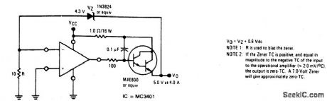
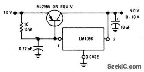
HIGH_STABILITY_1_A_REGULATOR
Published:2009/6/28 21:52:00 Author:May
View full Circuit Diagram | Comments | Reading(565)
74 Series digital circuit of 74190,74LS190 preset decimal reversible BCD counter(with mode control)
Published:2011/7/31 22:39:00 Author:Lucas | Keyword: 74 Series, digital circuit , preset decimal reversible , BCD counter, mode control

View full Circuit Diagram | Comments | Reading(3752)
Differential_16_channel_converter
Published:2009/7/25 4:49:00 Author:Jessie
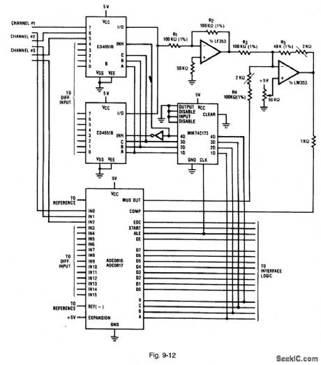
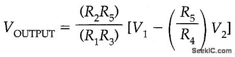
Figure 9-12 shows the ADC0816/17 connected to provide for an ADC with 16 differential inputs. This circuit is a modification of the circuit in Fig. 9-10. The CD4051 addressing is changed, and a differential amplifier is added between the multiplexer outputs and the comparator input. The select logic for the CD4051 is modified to enable the switches so that they can be selected in parallel with the ADC. The output of the three multiplexers are connected to a differential amplifier, composed of two inverting amplifiers with gain and offset trimmers. A dual op-amp configuration of inverting amplifiers can be trimmed easily, and has less-stringent feedback-resistor matching requirements (than a single op amp). The transfer equation for the dual op amp shown is:
The propagation delay through the op amps is an important consideration. There must be sufficient time between the analog switch-selection and start-conversion to allow the analog signal at the comparator input to settle. Using the LF353 op amp shown, the delay is about 5 pus. The op-amp gain and offset controls are adjusted to provide the zero and full-scale digital-output readings for the analog-in-put range or span. NATIONAL SEMICONDUCTOR, APPLICATION NOTE 258, P. 598. (View)
View full Circuit Diagram | Comments | Reading(986)
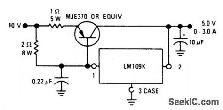
LOW_VOLTAGE_REGULATORS_WITH
Published:2009/6/28 21:51:00 Author:May
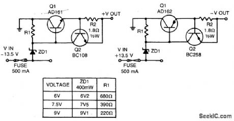
These short-circuit protected regulators give 6, 7.5, and 9 V from an automobile battery supply of 13.5 V nominal; however, they will function just as well if connected to a smoothed dc output from a transformer/rectifier circuit.Two types are shown for both positive and negative ground systems. The power transistors can be mounted on the heatsink without a mica insulating spacer thus allowing for greater cooling efficiency. Both circuits are protected against overload or short-circuits. The current cannot exceed 330 mA. Under normal operating conditions the voltage across R2 does not rise above the 500 mV necessary to turn Q2 on and the circuit behaves as if there was only Q1 present. If excessive current is drawn, Q2 turns on and cuts off Q1, protecting the regulating transistor. The table gives the values of R1 for different zener voltages. (View)
View full Circuit Diagram | Comments | Reading(1125)
CD_IGNITION
Published:2009/6/28 21:50:00 Author:May
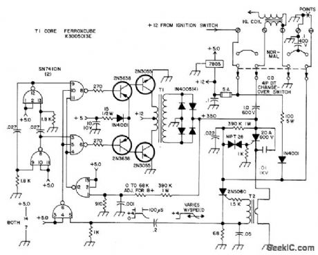
Uses master oscillator-power amplifier type of DC/DC converter in which two sections of triple 3-input NANDgate serve as 10 kHz square-wave MVBR feeding class B PNP/ NPN power amplifier through two-gate driver. Remaining two gates are used as logic invert-ers. Secondary of T1 has t5.24 meters of No. 26 in six bankwindings, with 20tums No. 14 added and center-tapped for primary. T2 is unshielded iron-core RF choke, 30-100 pH, whh several turns wound over it for secondary. When main 20-A SCR fires, T2 develops oscillation burst for firing sensitive gate-Iatching SCR. Storage ca-pacitor energy is then dumped into ignition coil primary through power SCR.-K. W. Robbins, CD Ignition System, 73 Magazine, May 1974, p 17and19. (View)
View full Circuit Diagram | Comments | Reading(1590)
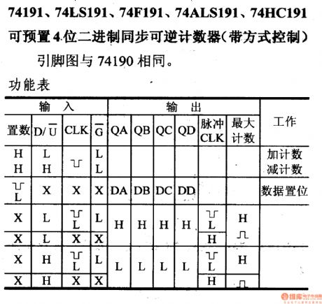
74 Series digital circuit of 74191, 74LS191 preset 4-bit synchronous reversible binary counter(with mode control)
Published:2011/7/31 23:05:00 Author:Lucas | Keyword: 74 Series, digital circuit , preset 4-bit synchronous , reversible binary counter, mode control
View full Circuit Diagram | Comments | Reading(2175)
VOLTAGE_REGULATOR
Published:2009/6/28 21:49:00 Author:May
View full Circuit Diagram | Comments | Reading(0)
10_MHz_UNIVERSAL_COUNTER
Published:2009/6/28 21:48:00 Author:May
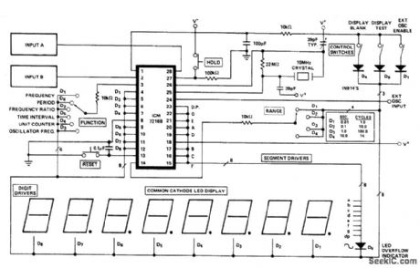


Circuit NotesThis is a minimum component complete Universal Counter. It can use input frequencies up to 10 MHz at INPUT A and 2 MHz at INPUT B. If the signal at INPUT A has a very low duty cycle, it may be necessary to use a 74121 monostable multivibrator or similar circuit to stretch the input pulse width to be able to guarantee that it is at least 50 ns in duration. (View)
View full Circuit Diagram | Comments | Reading(3510)
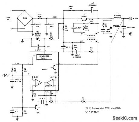
10_V/025_A_SWITCH_MODE_CONVERTER
Published:2009/6/28 21:48:00 Author:May
View full Circuit Diagram | Comments | Reading(679)
50_V/30_A_REGULATOR
Published:2009/6/28 21:46:00 Author:May
View full Circuit Diagram | Comments | Reading(639)
50_V/10_A_REGULATOR
Published:2009/6/28 21:45:00 Author:May
View full Circuit Diagram | Comments | Reading(613)
ELECTRIC_VEHICLE_CONTROL
Published:2009/6/28 21:45:00 Author:May


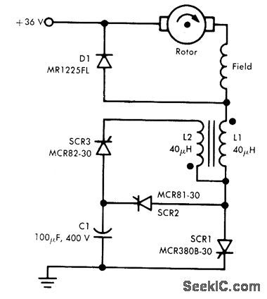
SCR1 is used in combination with Jones chopper to provide smooth acceleration of golf cart or other electric vehicle operating from 36-V on-board storage battery. Normal running current of 2-hp 36-V series-wound DC motor is 60 A, with up to 300 A required for starting vehicle up hill. Chopper and its control maintain high average motor current while limiting peak current by increas-ing chopping frequency from normal 125 Hz to as high as 500 Hz when high torque is required.-T. Malarkey, You Need Precision SCR Chopper Control, New Motorola Semiconduc-tors for Industry, Motorola, Phoenix, AZ, Vol, 2, No. 1, 1975. (View)
View full Circuit Diagram | Comments | Reading(1559)
Voltage_controlled_oscillator_frequency_sweep_operation
Published:2009/7/25 4:46:00 Author:Jessie
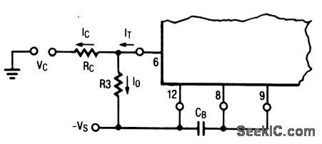
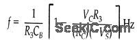

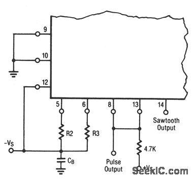
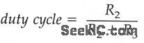
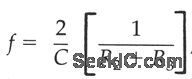
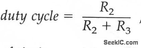
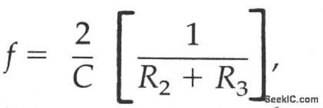
This circuit shows the connections required to convert the circuits of Figs. 5-52 and 5-53 to pulse and sawtooth operation. The duty cycle of the output waveforms is given as:and can be varied from 0.1% to 99.9% by proper choice of timing resistors. The frequency of oscillation is given as:
and can be modulated or swept by connecting R2 and R3 to common control voltage Vc instead of -Vs. (View)
View full Circuit Diagram | Comments | Reading(863)
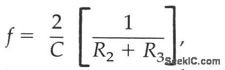
74 Series digital circuit of 74LS168A/169A preset 4-bit synchronous reversible counter
Published:2011/7/28 22:42:00 Author:Lucas | Keyword: 74 Series , digital circuit , preset 4-bit synchronous , reversible counter
168 is preset carry lookahead reversible decimal counter; 169 is preset carry lookahead reversible binary counter; count and preset are fully synchronized; it can be carry lookahead when fast counting; it can be used for n-bit binary cascade output; the clock circuit is fully independent.
(View)
View full Circuit Diagram | Comments | Reading(1217)
Simple_8_differential_channel_ADC
Published:2009/7/25 4:46:00 Author:Jessie
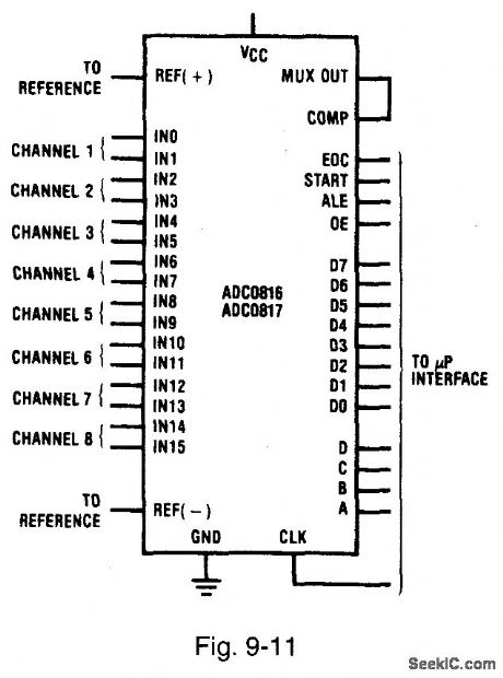
Figure 9-11 shows the ADC0816/17 connected to provide for an ADC with eight differential inputs. The differential inputs are implemented in software. All 16 channels are paired into positive and negative inputs. Then the control logic or microprocessor converts each channel of a differential pair, loads each result, then subtracts the two results. This method requires two single-ended conversions to do one differential conversiqn. As a result, the effective differential-conver sion time is twice that of a single channel, or a little more than 200 μs (assuming a clock of 640 kHz). The differential inputs should be stable throughout both conversions to produce accurate results. NATIONAL SEMICONDUCTOR, APPLICATION NorE 258, 1994, P. 597.
(View)
View full Circuit Diagram | Comments | Reading(701)
Simple_32_channel_ADC
Published:2009/7/25 4:44:00 Author:Jessie
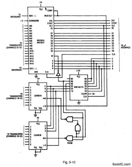
Figure 9-10 shows the ADC0816/17 connected to provide for 32-channel conversion. Such a configuration is possible because of the EC pin, which is actually a multiplexer enable. When the EC signal is low, all switches are inhibited so that another signal can be applied to the comparator input. Additional channels can be implemented as necessary. A total of five address lines are required to address the 32 channels. The lower four bits are applied directly to the A, B, C, and D inputs, All four bits are also applied to an MM74C174 flip-flop which is used as an address latch for the two CD4051s. The 1Q, 2Q, and 3Q outputs of the flip-flop feed the CD4051 address inputs. The 4Q and 5Q outputs are gated to form enable signals for each CD4051. Output 5Q is also applied at the EC input (after inversion) to enable the ADC multiplexer. NATIONAL SEMICONDUCTOR, APPLICATION NOTE 258, 1994, P. 596.
(View)
View full Circuit Diagram | Comments | Reading(961)
Eliminating_input_gain_adjustments
Published:2009/7/25 4:43:00 Author:Jessie
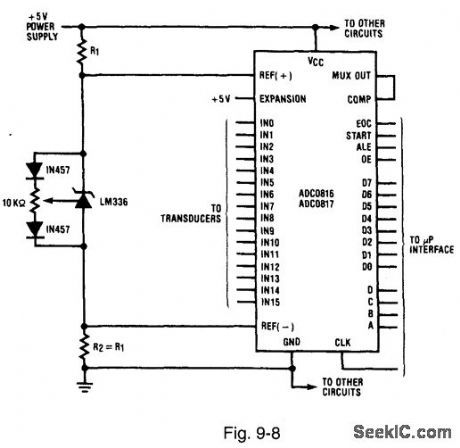
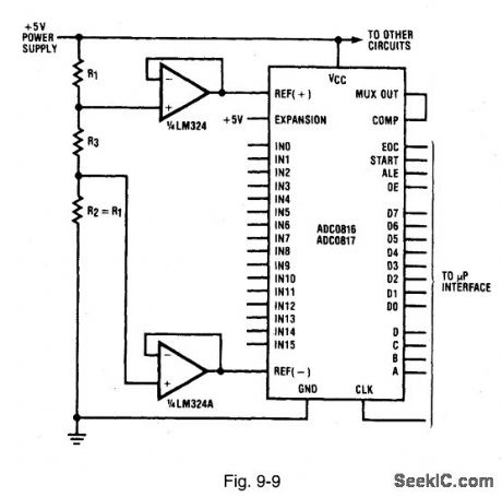
Figures 9-8 and 9-9 show the ADC0816/17 connected to eliminate gain adjustments on the analog input signals. This is done by varying the ADC REF+ and REF- voltages to get various full-scale ranges Typically, the reference voltages can be varied from 5 V to about 0.5 V to accommodate various input voltages. However, there is a restriction: the center of the reference voltage must be within 10.1 V of mid-supply. The reason for this restriction is that the reference ladder is tapped by an N-channel or P-channel MOSFET switch tree (Fig. 9-1), Offsetting the voltage at the center of the switch tree from VCC2 causes the transistors to turn off at the wrong point, resulting in inaccurate and erratic conversions. However, if properly applied, this method can reduce parts count and eliminate extra power Supplies for the input buffers. In the supply-centered reference circuit of Fig. 9-8, R1 and R2 offset REF+ and REF- from VCC and ground. An LM336-2.5 is shown, but any reference betueen 0.5 V and 5 V can be used. For odd reference values, use the op-amp circuit of Fig. 9-9. Single-supply op amps, such as the LM324 or LM10, can be used. R1, R2, and R3 form a resistor divider in which R1 and R3 center the reference at VCC2 and R2 can be varied to get the proper reference magnitude. NATIONAL SEMICONDUCTOR, APPLICATION NOTE 258, 1994, P. 595. (View)
View full Circuit Diagram | Comments | Reading(683)
74 Series digital circuit of 74167 BCD synchronization coefficient multiplier
Published:2011/7/29 1:14:00 Author:Lucas | Keyword: 74 Series, digital circuit, BCD , synchronization coefficient multiplier
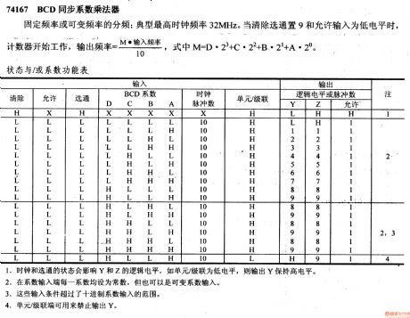
The fractional frequency has the fixed frequency or variable frequency; the typical maximum clock frequency is 32MHz. When the clear strobe sets to 9 and it allows the input to be low, the counter starts to work. 1. The status of clock and strobe has the effect on the logic level Y and Z, for example, unit/ cascade is low, the output Y remains high. 2. Each factor of the factor inputs is set to constant, but also can be a variable factor input. 3. The input conditions have been greater than the decimal input range. 4. Unit/cascade can be used to disable the output terminal Y.
(View)
View full Circuit Diagram | Comments | Reading(1353)
DAC_controlled_ctmplifier
Published:2009/7/25 5:34:00 Author:Jessie
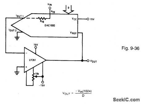
Figure 9-36 shows a DAC1000 connected to control the output of an LF351 amplifier. In this circuit, the DAC is used as the feedback element for an inverting amplifier. The R-2R ladder digitally adjusts the amount of output signal fed back to the amplifier summing junction. The feedback resistance can be thought of as varying from about 15 kΩ to infinity when the input code changes from full-scale to zero. The internal feedback resistor is used as the amplifier input resistor. When the input code is all 0s, the feedback loop is opened and the op-amp output saturates. NATIONAL SEMICONDUCTOR, APPLICATION NorE 271, 1994, P. 667. (View)
View full Circuit Diagram | Comments | Reading(649)
| Pages:1275/2234 At 2012611262126312641265126612671268126912701271127212731274127512761277127812791280Under 20 |
Circuit Categories
power supply circuit
Amplifier Circuit
Basic Circuit
LED and Light Circuit
Sensor Circuit
Signal Processing
Electrical Equipment Circuit
Control Circuit
Remote Control Circuit
A/D-D/A Converter Circuit
Audio Circuit
Measuring and Test Circuit
Communication Circuit
Computer-Related Circuit
555 Circuit
Automotive Circuit
Repairing Circuit