
Circuit Diagram
Index 1273
Voltage_controlled_oscillator_split_supply
Published:2009/7/25 4:36:00 Author:Jessie

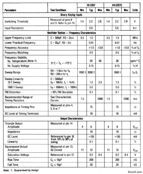
This circuit shows the baisc connection for an XR-2207 connected for split-supply operation. The output frequency(both sine and triangle) is controlled by C (pin2/3)and R1 through R4 .If a single timing resistors is used, the frequency is 1/RC. Otherwise ,the frequency is either 1/(R1//R2)C or 1/(R1//R4)C. Timing resistors R1 through R4 are activated by the logic signals at the binary keying input (pin 8/9),as shown in Fig,5-52B.Figure 5-52C shows the electrical characteristics. (View)
View full Circuit Diagram | Comments | Reading(788)
Absolute_conversion
Published:2009/7/25 4:34:00 Author:Jessie
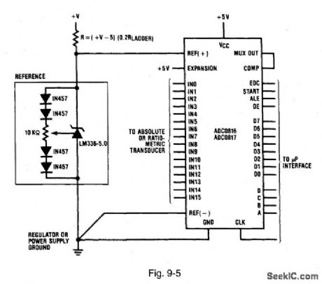
Figure 9-5 shows the ADC0816/17 connected for simple absolute conversion. Absolute conversion refers to the use of transducers with which the output value is not related to another voltage. The absolute value of the output voltage is very important (in contrast to the output voltage of a ratiometric transducer). This implies that the reference must be accurate to determine the value of the absolute output of the transducer. A precise, adjustable reference is provided by an LM336-5.0 and the associated parts. Ratiometric transducers can also be used in this circuit, and in most of the following data-conversion circuits. However, the key point to remember is that accuracy of absolute conversion depends primarily on the accuracy of the reference voltage. With ratiometric systems (Fig. 9-4), accuracy is determined by the transducer characteristics. NATIONAL SEMICONDUCTOR, APPLICATION NOTE 259, 1994, P. 594. (View)
View full Circuit Diagram | Comments | Reading(722)
PRECISION_HIGH_VOLTAGE_REGULATOR
Published:2009/6/28 22:07:00 Author:May
View full Circuit Diagram | Comments | Reading(2236)
POWER_PACK_FOR_BATTERY_POWERED_CALCULATORS,RADIOS,OR_CASSETTE_PLAYERS
Published:2009/6/28 22:07:00 Author:May
This circuit gives a regulated output of between 5 V and 15 Vdc, adjusted and set by a preset resistor. Current output up to about 350 mA. An integrated circuit regulates the output voltage and although this IC (the 7805) is normally used in a fixed-voltage (5 Vdc) supply it is for a variable output voltage. (View)
View full Circuit Diagram | Comments | Reading(743)
Ratiometic_conversion
Published:2009/7/25 4:32:00 Author:Jessie
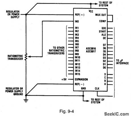
Figure 9-4 shows the ADC0816/17 connected for ratiometric conversion. Becauseboth ends of the 256R resistor ladder are available externally (Fig.9-1) the ICs areideally suited for use with ratiometric transducers A ratiometric transducer is aconverslon device in which the output is proportional to so me arbitrary full-scalevalue.The actual value of the transducer output is of no great importance but theratio of this output to the full-scale reference is valuable.The prime advantage of a ratiometric transducer is that an accurate reference is not essential However the reference should be nolse free because the voltage spikes during a converslon could cause inaccurate results.The circuit of Fig.9-4 uses the existing 5-V supply for reference thus eliminating the need for a special external reference. Take careto reduce power-supply nolse,The supply lines should be bypassed and separate PC traces shodld be used to route the 5-V and ground to the reference inputs andto the supply pms (if practical). NATIONAL SEMICONDUCTOR APPLICATION NOTE258 1994. P.592.
(View)
View full Circuit Diagram | Comments | Reading(703)
FIELD_STRENGTH_AT_7_MHz
Published:2009/6/28 22:04:00 Author:May

Operates from single dry cell, Meter can be calibrated in decibels with Hewlett-Packard 606A or equivalent signal generator,Jack permits remote metering L1 is 5 turns、and L2 is 30 turns wound onAmidonT68-2 core.-R,W Jones、A7-MHz Vertical Parasitic Array QST,Nov,1973、p 39-43and 52 (View)
View full Circuit Diagram | Comments | Reading(753)
33_V_5_V_and_12_V_from_six_to_twelve_cells
Published:2009/7/25 4:29:00 Author:Jessie
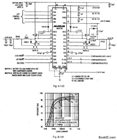
Figttre 8-130 shows a MAX782 notebook SMPS connected to provide 3.3 V, 5 V, and 12 V from six to twelve battery cells. Figure 8-131 shows the efficiency curves. The input voltage range is 5.5 V to 30 V, quiescent current (VIN = 15 V) is 420 μA, maximum load current (5-V output, VIN = 6) and 3.3-V output, VIN = 6 V) is 3 A, and the shutdown current is 70 μA. An evaluation kit is available from Maxim. MAXIM BATTERY MANAGEMENT CIRCUIT COLLECTION, 1994, P. 37. (View)
View full Circuit Diagram | Comments | Reading(549)
The duty cycle adjustable square wave generator circuit composed of 555
Published:2011/7/24 1:51:00 Author:Seven | Keyword: duty cycle, square wave generator
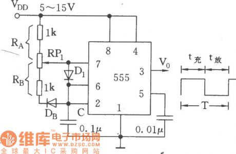
Once the circuit was added with a voltage VDD, the oscillator would start the oscillate. When the circuit is connected, as the voltage on C can't mutate, i.e the 2-pin LEV is the earth LEV firstly, which makes 555 offset, 3-pin is in a high LEV. C charges the generator through RA and D1, the charge time is tc=0.693RAC, when the voltage on C rises to 2/3VDD, 555 is reset, 3-pin is in a low LEV, at this moment, C discharge with the help of D1, R8 and the discharge tube in 555, the discharge time is td=0.693RbC. (View)
View full Circuit Diagram | Comments | Reading(2639)
5_A_CONSTANT_VOLTAGE/CONSTANT_CURRENT_REGULATOR
Published:2009/6/28 22:04:00 Author:May
View full Circuit Diagram | Comments | Reading(1134)
System_voltage_monitor
Published:2009/7/25 4:26:00 Author:Jessie
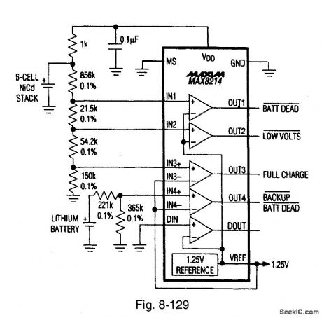
Figure 8-129 shows a MAX8214 voltage monitor connected to monitor the condition of a six-cell NiCad stack and a lithium backup battery. Larger portable systems often require several voltage-monitoring comparators to detect the status of main and backup batteries, as well as for power-fail monitoring and ac adapter detection. This circuit performs such monitoring and draws only 3 μA per comparator. The input-voltage range for the monitored voltage is 1.25 V to 100 V, and 2.7 V to 11 V for the IC. Quiescent current (VIN = 5 V) is 16 μA, and threshold accuracy is 11% maximum. When the NiCad stack is fully charged, output 3 goes high. When the NiCad stack voltage drops to a low (but still usable) level, output 2 goes low. When the NiCad stack is dead, output 1 goes low. Output 4 goes low when the lithium battery is dead. MAXIM BATTERY MANAGEMENT CIRCUIT COLLECTION, 1994, P. 77. (View)
View full Circuit Diagram | Comments | Reading(730)
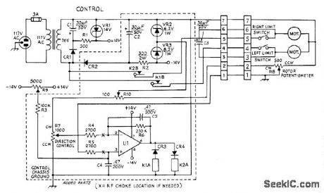
ANTENNA_POSITION_CONTBOL
Published:2009/6/28 22:03:00 Author:May
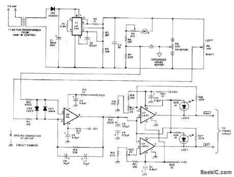
IC logic provides automatic brake release and poshitive povsition control for commercial Ham-M antenna rotator Regulated power supply drives bridge haing position-sensing pot R8 in rotator and R9 in control box When antenna is in desired position, wiper voltages of pots are equal.When R9 is set to new position, voltage difference is amplified by error amplifier U2. Comparators U3 and U4 determine rotation direction needed for rebalance and delivet logic circuits to timing circuit (also given in article) that drives motor and brake release relays.Timer prevents jamming of circuit by operator error.-P. Zander, Automatic Position Control for the HAM-M Rotator, Ham Radio, May 1977, p 42-45. (View)
View full Circuit Diagram | Comments | Reading(2549)
Complete_function_generator
Published:2009/7/25 4:25:00 Author:Jessie
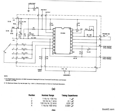
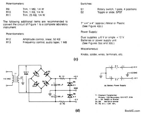
This circuit uses an XR-2206 to provide sine, triangle, and square outputs that can be AM/FM modulated. There are four overlapping frequency ranges selected by S1, as shown in Fig. 5-51B. The parts list, and a typical power supply, are shown in Figs. 5-51C and 5-51D respectively. Each tuning range can be varied over a 100:1 range. The sine/triangle output (P) can be varied from 0 to over 6 Vpp and appears as a 600-Ω source at the output terminal. The square-wave output (full M, or half L) is available for scope sync or to drive logic circuits. S1 selects range, S2 selects triangle or sine output, R9 sets dc-offset level of the triangle or sine output, R10 is adjusted for minimum harmonic content of the sine output. R11 is adjusted for optimum symmetry of the sine output. R12 sets the amplitude of the triangle/sine output, and should be a front-panel control, as should R13, which varies the frequency over the 100:1 range. To adjust for minimum distortion, monitor the output at P with S2 closed. Set R12 for a non-clipping maximum swing, then adjust R10 and R11 alternately for minimum distortion. Use a distortion meter, if desired, for final adjustment. Typical distortion is less than 1% from 1 Hz to 10 kHz, and less than 3% over the entire range. (View)
View full Circuit Diagram | Comments | Reading(3042)
High_side_current_sense_amplifier
Published:2009/7/25 4:25:00 Author:Jessie
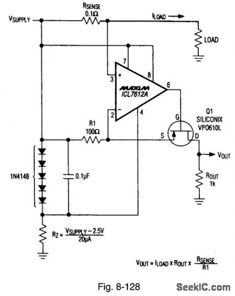
Figure 8-128 shows an ICL7612A micropower op amp connected to provide sensing of high-side current. The operating voltage range is 4.5 V to 48 V, quiescent current (VIN = 5 V) is 20 μA, and the gain factor is 1 VA. The circuit senses current in the positive battery lead, allowing the battery's negative terminal to be directly connected to circuit ground. The circuit output is a ground-referenced output voltage that is directly proportional to the current flowing in the low-value sense resistor. The output is typically added to the input of an A/D converter or integrating V/F converter. Because the output current is a true-current source, the output can be referenced to any level within the supply limits. The value of R1 should be kept in the range of 100 × RSENSE to 1000× RSENSE. MAXIM BATTERY MANAGEMENT CIRCUIT COLLECTION, 1994, P. 75.
(View)
View full Circuit Diagram | Comments | Reading(1266)
12_V_TO_9,75_or_6_V_CONVERTER
Published:2009/6/28 22:02:00 Author:May
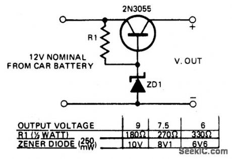
This circuit enables transistorized items such as radio, cassettes, and other electrical devices to be operated from a car's electrical supply. The table gives values for resistors and specified diode types for different voltage. Should more than one voltage be required a switching arrangement could be incorporated.For high currents, the transistor should be mounted on a heatsink. (View)
View full Circuit Diagram | Comments | Reading(523)
SELECTABLE_BANDWIDTH_NOTCH_FILTER
Published:2009/6/28 22:02:00 Author:May
Circuit Notes
This notch filter, which operates at up to 200 kHz, uses a modified Wien bridge to select bandwidth over which frequencies are rejected. RC components determine filter's center frequency, Plselects notch bandwidth. Notch depth is fixed at about 60 dB. (View)
View full Circuit Diagram | Comments | Reading(1052)
IC_rprecision_waveform_generator_with_sweep_and_frequency_modulation_
Published:2009/7/25 4:23:00 Author:Jessie
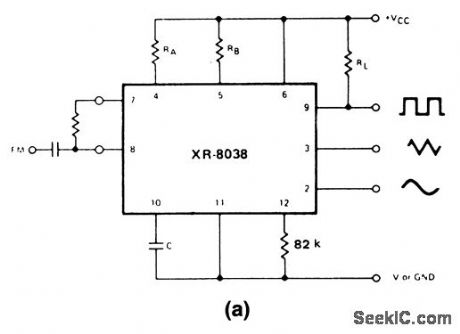
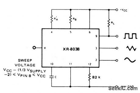
These circuits are similar to that of Fig. 5-47, except that the circuits provide for FM or sweep modulation. Use circuit 5-50A for FM (small deviations, about±10%). Use circuit 5-50B for a sweep range of 1000:1. As a guideline, the sweep frequency approaches 0 Hz when the voltage at pin 8 equals VCC, and reaches maximum at the lower pin-8 voltage limit of VCC - (1/3 VSUPPLY -2).Waveform symmetry variations can be minimized when a 10-M resistor is added between pins 5 and 11. (View)
View full Circuit Diagram | Comments | Reading(3227)
The tone changeable multivibrator circuit
Published:2011/7/24 1:57:00 Author:Seven | Keyword: tone changeable multivibrator, circuit

This tone changeable multivibrator circuit consists of the time-based circuit 555, which can emit the continuous changing oscillating wave of 400~2500Hz, like the police car sound. The circuit consists of the starting relay, low-frequency oscillator and modulating audio generator. (View)
View full Circuit Diagram | Comments | Reading(743)
VARIABLE_ZENER_DIODE
Published:2009/6/28 22:01:00 Author:May
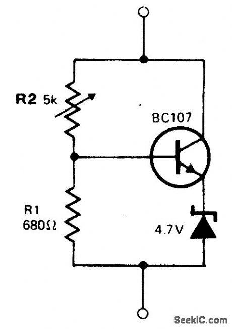
The circuit behaves like a zener diode over a large range of voltages. The current passing through the voltage divider R1-R2 is substantially larger than the transistor base current and is in the region of 8 mA. The stabilizing voltage is adjustable over the range 5-45 V by changing the value of R2. The total current drawn by the circuit is variable over the range 15 mA to 50 mA. This value is determined by the maximum dissipation of the zener diode. In the case of a 250 mW device, this is of the order of 50 mA. (View)
View full Circuit Diagram | Comments | Reading(201)
INSTANT_VSWR_BRIDGE
Published:2009/6/28 22:01:00 Author:May

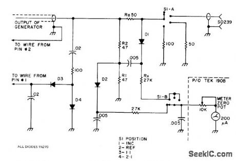
Modified 190B Tektronix constant-amplitude signal generator is combined with 50-ohm resistance bridge toglve stable high-accuracy instrument for measuring voltage standing-wave ratio as guide fortuning antennas Range iS 160 meters through 10 meters,Trim Rx so incident or forward voltage at position 1 of S1 equals reflected voltage at position 2. Article gives chart for finding VSWR. Step-by-step procedure for modifying signal generator is given.-D.Sander, Make Antenna Tuning a Joy, 73 Magazine, May 1978, p 134-136. (View)
View full Circuit Diagram | Comments | Reading(1166)
IC_precision_waveform_generator_with_minimum_sine_wave_distortion
Published:2009/7/25 4:22:00 Author:Jessie
This circuit is similar to that of Fig. 5-47, except that sine-wave distortion can be adjusted to less than 0.5%. (View)
View full Circuit Diagram | Comments | Reading(1224)
| Pages:1273/2234 At 2012611262126312641265126612671268126912701271127212731274127512761277127812791280Under 20 |
Circuit Categories
power supply circuit
Amplifier Circuit
Basic Circuit
LED and Light Circuit
Sensor Circuit
Signal Processing
Electrical Equipment Circuit
Control Circuit
Remote Control Circuit
A/D-D/A Converter Circuit
Audio Circuit
Measuring and Test Circuit
Communication Circuit
Computer-Related Circuit
555 Circuit
Automotive Circuit
Repairing Circuit