
Circuit Diagram
Index 1272
IC_function_generator_connected_for_sine_output_with_external_adjustment
Published:2009/7/25 3:59:00 Author:Jessie
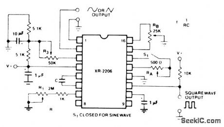
This circuit is similar to that of Figs. 5-31/5-32, except that the harmonic content of the sine output can be reduced to about 0.5%. Set RB at midpoint and adjust RA for minimum distortion. With RA set, adjust RB to further reduce distortion. If a triangle output is desired, open S1. (View)
View full Circuit Diagram | Comments | Reading(779)
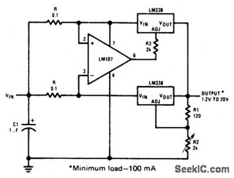
HIGH_VOLTAGE_REGULATOR(VSUBout_SUB=_7_V_TO_37_V)
Published:2009/6/28 22:19:00 Author:May
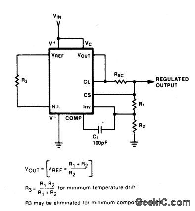
View full Circuit Diagram | Comments | Reading(528)
74 Series digital circuit of 74S226 4-bit parallel latched bus transceiver
Published:2011/7/31 22:37:00 Author:Lucas | Keyword: 74 Series, digital circuit , 4-bit parallel latched, bus transceiver
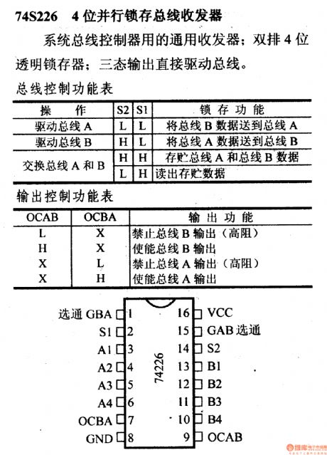
The universal transceiver for system bus controller; double 4-bit transparent latch; one state output can directly drive the bus.
(View)
View full Circuit Diagram | Comments | Reading(1119)
VSWR_BRIDGE
Published:2009/6/28 22:19:00 Author:May
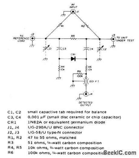
Works well through 450 MHz to for measuring and matching VHF and UHF antennas. If identical load impedances are placed at J2 and J3, signals at opposite ends of R3 are equal and in phase and there is no output at J4. If impedances are different, output proportional to difference appears at J4 Impedance values can be from 25 to 100 ohms, although drcuit is designed for optimum performance at 50 ohms.-J. Reisert, Matching Techniques for VHF/UHF Antennas, Ham Radio, July 1976, p 50-56. (View)
View full Circuit Diagram | Comments | Reading(1168)
MODULATION_MONlTOR
Published:2009/6/28 22:18:00 Author:May
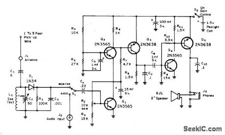
Provides off-the-air monitoring of RF signals up to 200 MHz by rectified detection of AM signals and by slope detection of FM signals. Can also be used as signal tracer, audio amplifier, orhidden-transmitter locator. High-gain audio amplifier has low-noise cascode input stage and output stage driving headphone or Ioudspeaker. S1 selects RF signals detected by D1 or AF applied to J2. L1 is 4 tums No. 18 for monitoring 75-150 MHz. Will also monitor VHF transmissions from pilot to ground stations while in commercial aircraft, using 24-inch wire antenna near window and earphone. Passive-type receiver is safe in aircraft because it has no oscillators that could interfere with navigation equipment. -W. F. Spli-chal, Jr., Sensitive Modulation Monitor, CQ, Jan. 1973, p 59-61. (View)
View full Circuit Diagram | Comments | Reading(2542)
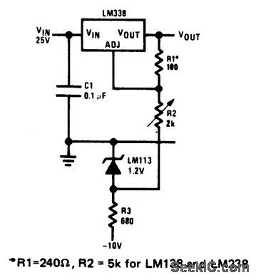
ADJUSTABLE_REGULATOR_O_10_V_AT_3_A
Published:2009/6/28 22:18:00 Author:May
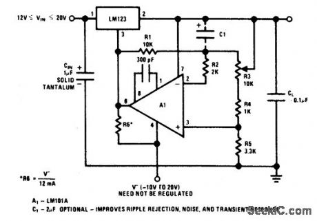
View full Circuit Diagram | Comments | Reading(630)
FIELD_STRENGTH_METER
Published:2009/6/28 22:18:00 Author:May
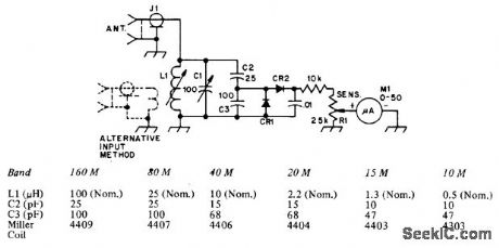
Useful for antenna experiments and ad justments in amateur bands from 160 to 10 meters. Increasing size of pickup antenna increases sensitivity. Far-field measurements are made with alternate input circuit, in which reference dipole or quarter-wave wire cut for frequency of interest is connected to input link. Diodes are 1N34A germanium or equivalent. M1 is 50μA. Table gives values of tuned-circuit components for six amateur bands.-D. DeMaw, A Simple Field-Strength Meter and How to Calibrate It, QST, Aug. 1975, p21-23. (View)
View full Circuit Diagram | Comments | Reading(5526)
The single stable circuit with changeable width
Published:2011/7/21 3:26:00 Author:Seven | Keyword: stable circuit, changeable width
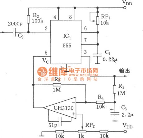
Usually, the single stable circuit outputs the solid pulse width. See as the figure, the circuit adopts the output pulse, after the pulse is low-pass filtered and DC amplified, the closed loop controls the 555 control terminal, the contemporary stable width will shrink automatically, so the cycle duty of the output waveform remains the same.
(View)
View full Circuit Diagram | Comments | Reading(639)
10_A_REGULATOR
Published:2009/6/28 22:17:00 Author:May
View full Circuit Diagram | Comments | Reading(692)
0_TO_22_V_REGULATOR_
Published:2009/6/28 22:17:00 Author:May
View full Circuit Diagram | Comments | Reading(674)
VOLTAGE_REGULATOR
Published:2009/6/28 22:17:00 Author:May
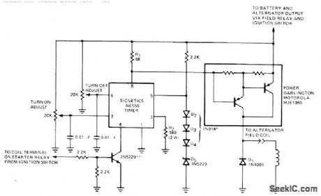
Time and power Darlington form simple automobile voltage regulator. When batteru voltage drops below 14.4 V , timer is turned on and Darlington pair conducts. Separate adjustments are provided for preset turn-on and turnoff voltages.- signetics Analog Data Manual. Signetics, Sunnyvale, CA, 1977, p 731. (View)
View full Circuit Diagram | Comments | Reading(0)
Voltage_controlled_oscillator_single_supply
Published:2009/7/25 4:40:00 Author:Jessie
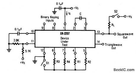
This circuit shows the basic connection for an XR-2207 connected for single-supply operation .The functions and electrical characteristics are as shown in Figs. 5-52B and 5-52C. (View)
View full Circuit Diagram | Comments | Reading(704)
Buffered_reference_used_as_a_power_supply
Published:2009/7/25 4:39:00 Author:Jessie
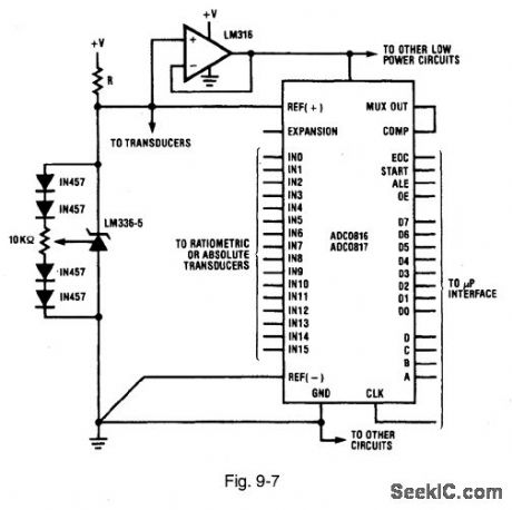
Figure 9-7 shows the ADC0816/17 used with a buffered reference. This method of buffering the reference provides higher current capabilities than the circuit of Fig. 9-6, and eliminates the IP term in the equation for resistor R. NATIONAL SEMICONDUCTOR, APPLICATION NOTE 258, 1994, P. 594. (View)
View full Circuit Diagram | Comments | Reading(713)
0_TO_30_V_REGULATOR
Published:2009/6/28 22:16:00 Author:May
View full Circuit Diagram | Comments | Reading(629)
REMOTE_SHUTDOWN_REGULATOR_WITH_CURRENT_LIMITING
Published:2009/6/28 22:16:00 Author:May
View full Circuit Diagram | Comments | Reading(670)
Using_the_referenc_as_the_supply
Published:2009/7/25 4:38:00 Author:Jessie
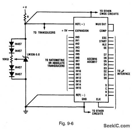
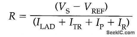
Figure 9-6 shows the ADC0816/17 connected with the external reference used asthe supply. The LM336-5.0 provides regulated 5-V for the ADC power andreference inputs as well as for the power input of other components in the system Of course an unregulated supply greater than 5 V is required for V+ Seriesresistor R is chosen so that the maximum current needed by the system is supplied and the LM336-5.0 is kept in regulation,The value of R is found by∶
where VS=unregulated supply voltage; VREF=reference voltage; ILAD =VREF/1 kΩ resistor ladder current; ITR =transducer currents IP=system power supply requirements; and IR = minimum reference current.NATIONAL SEMICONDUCTOR APPLICATION NOTE 258. 1994, P. 594.
(View)
View full Circuit Diagram | Comments | Reading(622)
HEADLIGHT_REMINDER_1
Published:2009/6/28 22:12:00 Author:May
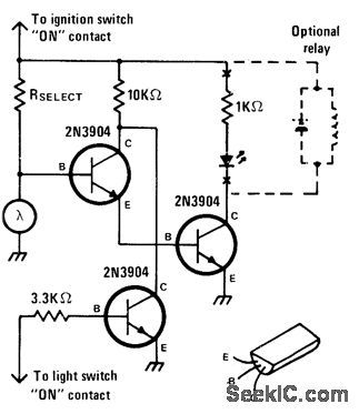
Photocell energizes circuit at twilight to remind motorist that lights should be turned on. Indicator can be LED connected as shown or relay turning on buzzer for more positive signal. Circuit can be made au-tomatic by connecting relay contacts in parallel with light switch, provided delay circuit is added to prevent oncoming headlights from killing circuit. Mount photocell in location where it is unaffected by other lights inside or outside car.-J. Sandier, 9 Projects under $9, Modern Electronics, Sept. 1978, p 35-39. (View)
View full Circuit Diagram | Comments | Reading(801)
74 Series digital circuit of 74198 8-bit shift register
Published:2011/7/29 1:26:00 Author:Lucas | Keyword: 74 Series , digital circuit , 8-bit shift register
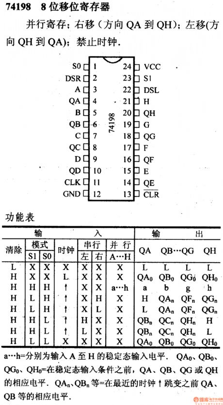
Parallel storage; right shift(direction is from the QA to QH): left shift(direction is from the QH to QA); it forbids the clock.
a. .. h= the input of steady-state input level of A to H.
QAo,QBo, QGo, QHo=the input of steady-state input level of QAo,QBo, QGo, QHo.
QAn, QBn= the corresponding level ofQA, QB before the next jump of the clock.
(View)
View full Circuit Diagram | Comments | Reading(2152)
TRANSISTORIZED_BREAKER_POINTS
Published:2009/6/28 22:09:00 Author:May
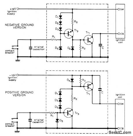
Uses Texas Instruments BUY23/23A high-voltage transistors that can easily withstand voltages up to about 300V existiong across breaker points of distributor in modern car. Circuit serves as electronic switch that isolates points fro;yt heavy interrupt current and high-voltage back-swing of Ignition coil, thereby almost completely eliminating wear on points. Values are: Tr2 2N3789; Tr3 (for positive ground version) 2N3055; D1-D4 1N4001; D5 18-V 400-mW zener; R1 56 ohm; R2 1.2 ohms; R3 10 ohms; C 600 VDC same size as points capacitor. Article covers installation procedure.-G.F. Nudd, Transistor-Aided Ignition, Wireless World, April 1975, p 191. (View)
View full Circuit Diagram | Comments | Reading(1640)
The low power single stable circuit
Published:2011/7/21 3:33:00 Author:Seven | Keyword: low power, single stable circuit
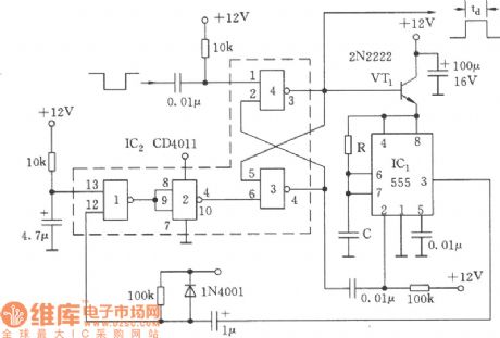
See as the figure, the circuit contains a 2-input terminal NAND CD4011 and a CMOS 555, so whether it is static or high LEV output timing period, the consuming power is very low. The door 3 and 4 of CD4011 compose the RS trigger. As the whole circuit is a closed circuit, the time pulse width is decided by the RC time constant, i.e td=1.1R1C1. (View)
View full Circuit Diagram | Comments | Reading(650)
| Pages:1272/2234 At 2012611262126312641265126612671268126912701271127212731274127512761277127812791280Under 20 |
Circuit Categories
power supply circuit
Amplifier Circuit
Basic Circuit
LED and Light Circuit
Sensor Circuit
Signal Processing
Electrical Equipment Circuit
Control Circuit
Remote Control Circuit
A/D-D/A Converter Circuit
Audio Circuit
Measuring and Test Circuit
Communication Circuit
Computer-Related Circuit
555 Circuit
Automotive Circuit
Repairing Circuit