
Circuit Diagram
Index 1266
Easy_tune_sine_wave_oscillator
Published:2009/7/25 3:29:00 Author:Jessie
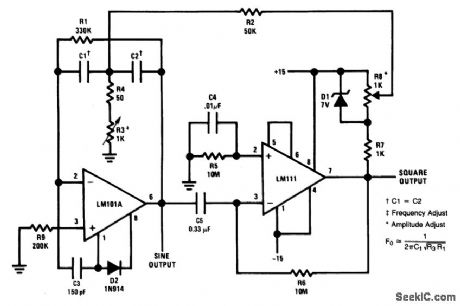
This circuit provides both sine- and square-wave outputs at frequencies from below 20 Hz to above 20 kHz, by varying R3. R8 sets amplitude.Distortion varies between 0.75% and 2% depending on R3 setting. The frequency range is set by R1, R3, and C1, as shown. (View)
View full Circuit Diagram | Comments | Reading(692)
DRIVER_CIRCUITS
Published:2009/6/28 23:11:00 Author:May
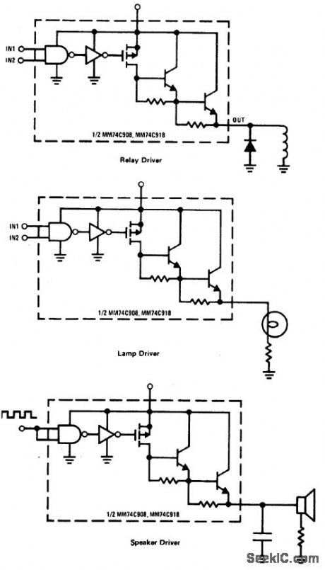
Circuit NotesCM0S drivers for relays, lmps,speakers,etc, offers extremely low standby power. At Vcc = 15V, power dissipation per package is typically 750 nW when the outputs are not drawing current. Thus, the drivers can be sitting out on line (a telephone line, for example) drawing essentially zero current until activated. (View)
View full Circuit Diagram | Comments | Reading(794)
1_Hz_to_1_MHz_sine_wave_VCO
Published:2009/7/25 3:27:00 Author:Jessie
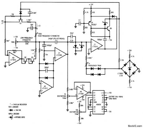
For a 0- to 10-V input, this circuit produces sine-wave outputs of 1 Hz to 1MHz, Both symmetry and distortion can be trimmed ndependently. (View)
View full Circuit Diagram | Comments | Reading(1134)
Low_frequency_sine_wave_generator
Published:2009/7/25 3:25:00 Author:Jessie
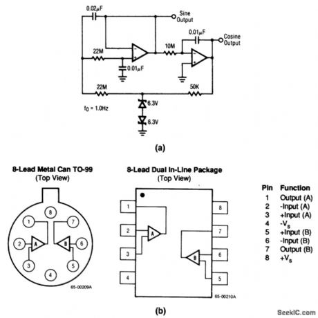
This circuit uses both sections of an RC4559 to form a 1-Hz sine-wave generator with both sine and cosine outputs. Figure 5-11B shows the pin connections. (View)
View full Circuit Diagram | Comments | Reading(0)
Triangle_and_square_wave_generator
Published:2009/7/25 3:24:00 Author:Jessie
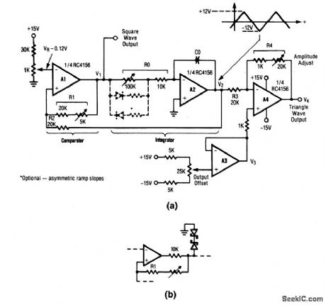
This circuit produces both triangle and square-wave outputs that can be adjusted independently. For best operation, set R1 and VR for a triangle at V2 with ±12-V amplitude. Then, adjust R4 for desired triangle output level. Triangle frequency is set by C0 and R0. Circuit should function well up to about 10 kHz. A more symmetrical waveform can be generated by adding a back-to-back Zener, as shown in Fig. 5-10B. (View)
View full Circuit Diagram | Comments | Reading(0)
The high speed switch power controller M62213FP switch regulated power supply circuit
Published:2011/7/24 4:05:00 Author:Seven | Keyword: high speed, controller, power supply
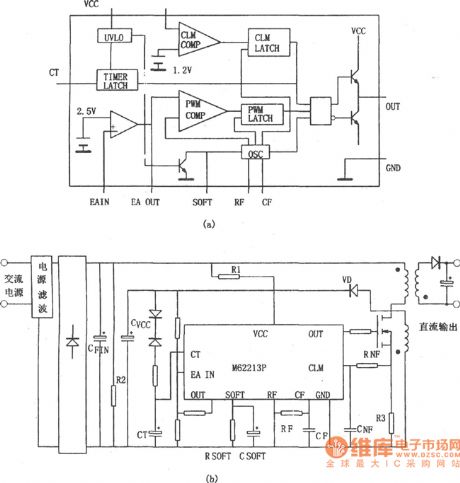
In Figure (b) is a switch regulated power supply composed of high speed switch power controller M62213FP. The conducting time of the power supply output pulse is decided by the SOFT resistor, if a capacitor is parallel with the resistor, the starting time will be prolonged, so the soft start can be fulfilled. When M62213FP is starting, the working voltage of it is provided by R1 after the AC power supply voltage is rectified.
Figure1 the internal structure of M62213FP
(View)
View full Circuit Diagram | Comments | Reading(607)
Pulse_generator_astable_multivibrator
Published:2009/7/25 3:23:00 Author:Jessie
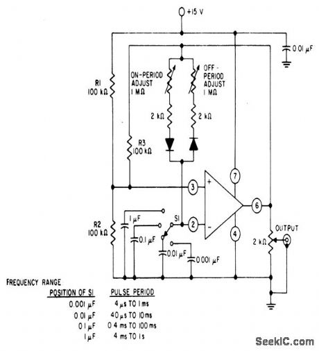
This circuit provides independent control of both On and Off periods, as well as the pulse period. (View)
View full Circuit Diagram | Comments | Reading(615)
REGULATOR_FOR_ALTERNATOR
Published:2009/6/28 23:09:00 Author:May
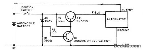
Simple and effective solid-state replaeement for auto voltage regulator can be used with altemator in almost any negative-ground system. Circuit acts as switch supplying either full or no voltage to field winding of altemator. When battery is below 13 V, zenel D1 does not conduct, Q1 is off, Q2 is on, and full battery voltage is applied to alternator field so it puts out full voltage to battery forcharging. When battery reaches 13.6 V, Q1 tums on, Q2 tums off, altemator output is reduced to zero, and battery gets no charging current. Corcuit can also be used with wind-drivent alternator systems.-P.S.Smith, $22 for a Regulator? Never!, 73 Magazine, Holifay issue 1976, p 103. (View)
View full Circuit Diagram | Comments | Reading(4155)
Staircase_generator
Published:2009/7/25 3:22:00 Author:Jessie
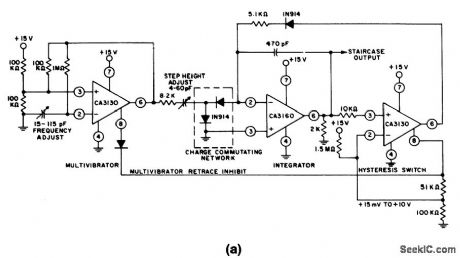
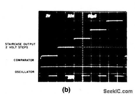
Both the frequency and step height can be adjusted separately in this circuit. Figure 5-8B shows the waveforms for each section. (View)
View full Circuit Diagram | Comments | Reading(0)
DUAL_RANGE_RF_WATTMETER
Published:2009/6/28 23:07:00 Author:May
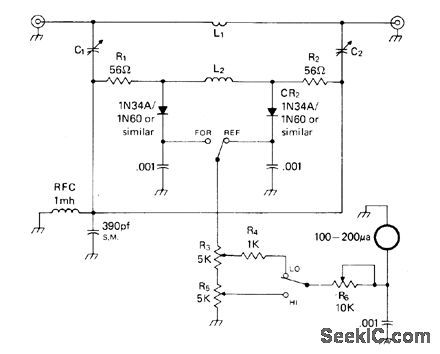
Uses circuit which is not frequency-sensitive, so calibration can be accurate over wide frequency spectrum, Ranges are 0-1 and 0-10 W. L2 is 7-50-2 toroid wound almost full with No. 28 enamel, leaving only room for 2-tum link L1.C1 and C2 are 3-20 pF trimmers. Article covers calibiation and use and gives table for reading SWR by comparing watts FORWARD with watts REFLECTED,-A,Weiss、The Silk-Purse In-Line Wattmeter、CQ,May 1977 p 50-52 and 74-75 (View)
View full Circuit Diagram | Comments | Reading(1428)
Precision_VCO
Published:2009/7/25 3:21:00 Author:Jessie
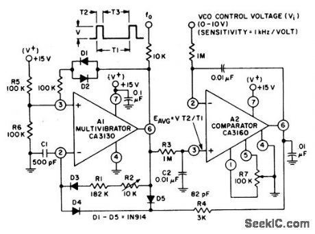
This voltage-controlled oscillator operates with a tracking error in the order of 0.02%、and a temperature coefficient of 0.01%/℃.Adjust both R2 and R7 for an output sensitivity of 1-kHz/V(from 0-to 10-V input) (View)
View full Circuit Diagram | Comments | Reading(838)
FIELD_STRENGTH_METER_2
Published:2009/6/28 23:07:00 Author:May
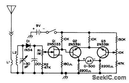
Developed for tuning all types of antennas, from mobile whips to four-element quads. Avoids shielding and other problems of switched T pads for calibrated attenuator by first detecting RF, then attenuating DC output. Technique has added advantage that circuit is no longer frequency-sensitive. To cover 13-24 MHz, L2 is 11 tums spaced out to about 1 inch, with 2 turns overtop for L1. D1 can be any diode such as 1N34. R1 serves as calibrated attenuator, with R2 in series giving 0-dB point at junction. Article covers construction and operation.-J. L. liffe, An Amplified, Cali-brated, Signal Strength Meter, 73 Magazine, June 1973, p 85-86. (View)
View full Circuit Diagram | Comments | Reading(1248)
Function_generator_with_wide_tuning_range
Published:2009/7/25 3:19:00 Author:Jessie
The adjustment range of this generator is in excess of 1,000,000/1, using a single frequency-adjust potentiometer, or an external voltage-control source.Both the pulse amplitude and triangle-wave slope symmetry can be adjusted individually. (View)
View full Circuit Diagram | Comments | Reading(1)
TUNED_RADIATED_FIELD_METER
Published:2009/6/28 23:06:00 Author:May
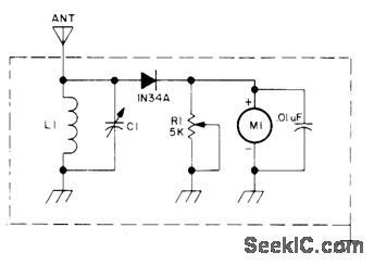
Provides quick check of transmitter performance and approximate check offrequency,Valuesfor L1 and C1 are chosen to cover desired frequency range,Metercan be 1 mA or 200μA,Keep lead lengthsshort-E.Hartz Is My Rig Working or Not?、73Magazine. Oct 1976、p 56-57 (View)
View full Circuit Diagram | Comments | Reading(738)
FIELD_STRENGTH_METER_1
Published:2009/6/28 23:05:00 Author:May
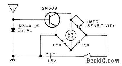
Easily assembled for checking performance of amateur radio transmitter and its antenna system.-Circuits, 73 Magazine, Jan. 1974, p 128. (View)
View full Circuit Diagram | Comments | Reading(643)
Voltage_controlled_sine_wave_oscillator
Published:2009/7/25 3:18:00 Author:Jessie
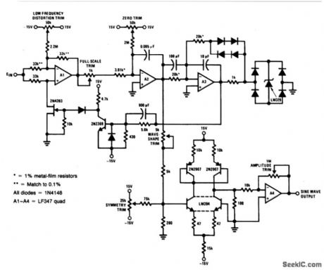
For a 0- to 10-V input, this circuit produces sine-wave outputs of 1 Hz to 20 kHz, with better than 0.2% linearity. Distortion is about 0.4% and the sine-wave output frequency and amplitude settle instantaneously to a step-input change. To calibrate, apply 10 V to the input and adjust the wave-shape trim and symmetry trim for minimum distortion on a distortion analyzer. Next, adjust the input voltage for an output frequency of 10 Hz and trim the low-frequency distortion for minimum indication on the distortion analyzer. Finally, alternately adjust the zero and full-scale pots so that inputs of 500μV and 10 V yield respective outputs of 1 Hz and 20 kHz. (View)
View full Circuit Diagram | Comments | Reading(2192)
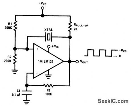
Crystal_controlled_square_wave_oscillator
Published:2009/7/25 3:17:00 Author:Jessie
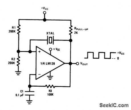
In this circuit, the values of R1 and R2 are equal so that the LM139 comparator switches symmetrically about +Vcc/2. To ensure a 50% duty cycle, the RC time constant of R3 and C1 is set to be several times greater than the period of the oscillating frequency (which depends on the crystal resonant frequency).When specifying the crystal, order series-resonant, along with the desired temperature coefficient and load capacitances to be used.
(View)
View full Circuit Diagram | Comments | Reading(1401)
The single knot transistor pulse transformer trigger thyristor circuit
Published:2011/7/21 3:15:00 Author:Seven | Keyword: single knot transistor, pulse transformer
View full Circuit Diagram | Comments | Reading(1324)
Pulse_generator_with_variable_duty_cycle
Published:2009/7/25 3:15:00 Author:Jessie
In this circuit, time t1 (pulse width) is set by R4, while time t2 (frequency) is set by R5. 1N914 or equivalent diodes can be used and D2. (View)
View full Circuit Diagram | Comments | Reading(0)
50_MHz_trigger
Published:2009/7/25 3:13:00 Author:Jessie
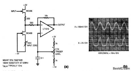
In this circuit, the FETs form a simple high-speed buffer and the LT1016 compares the buffer output to the voltage set by the trigger-level pot. The circuit has a 100-mV sensitivity at 50 MHz. Figure 5-2B shows the trigger response (trace B) to a 50-MHz sine wave (trace A). To calibrate, ground the input and adjust the input-zero control for 0 V at the Q2 drain terminal. (View)
View full Circuit Diagram | Comments | Reading(1706)
| Pages:1266/2234 At 2012611262126312641265126612671268126912701271127212731274127512761277127812791280Under 20 |
Circuit Categories
power supply circuit
Amplifier Circuit
Basic Circuit
LED and Light Circuit
Sensor Circuit
Signal Processing
Electrical Equipment Circuit
Control Circuit
Remote Control Circuit
A/D-D/A Converter Circuit
Audio Circuit
Measuring and Test Circuit
Communication Circuit
Computer-Related Circuit
555 Circuit
Automotive Circuit
Repairing Circuit