
Circuit Diagram
Index 1456
Computer motherboard circuit 810 2_04
Published:2011/7/27 1:33:00 Author:Ecco | Keyword: Computer motherboard
View full Circuit Diagram | Comments | Reading(688)
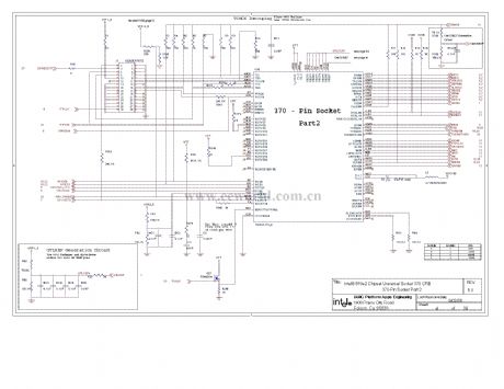
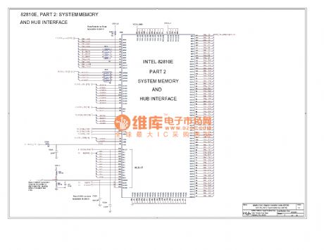
Computer motherboard circuit 810 2_05
Published:2011/7/27 1:33:00 Author:Ecco | Keyword: Computer motherboard
View full Circuit Diagram | Comments | Reading(597)
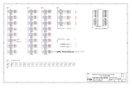
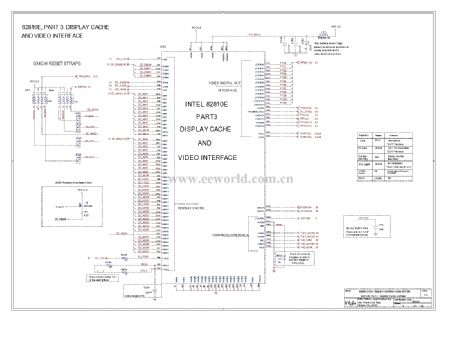
Computer motherboard circuit 810 2_06
Published:2011/7/27 1:34:00 Author:Ecco | Keyword: Computer motherboard
View full Circuit Diagram | Comments | Reading(699)
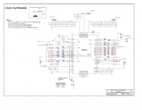
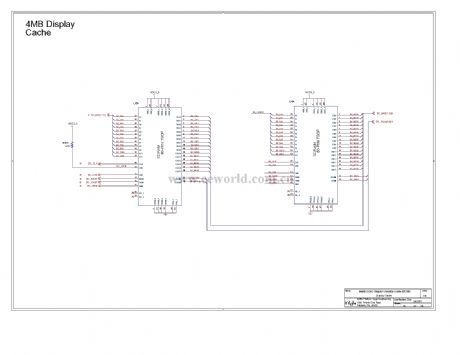
Computer motherboard circuit 810 2_07
Published:2011/7/27 1:34:00 Author:Ecco | Keyword: Computer motherboard
View full Circuit Diagram | Comments | Reading(661)
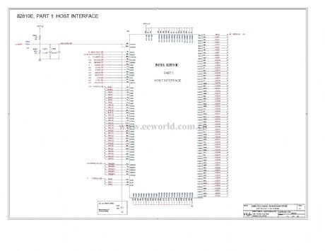
Computer motherboard circuit diagram 810 2_08
Published:2011/7/27 1:35:00 Author:Ecco | Keyword: Computer motherboard
View full Circuit Diagram | Comments | Reading(667)
Improved one-shot timer circuit composed of 2 PUT
Published:2011/5/8 11:11:00 Author:Rebekka | Keyword: Improved one-shot timer
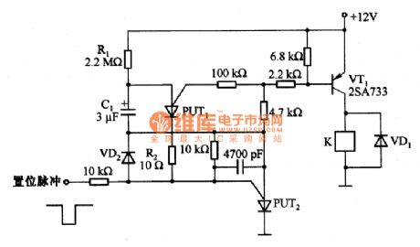
Figure 1 is an improved trigger timing circuit composed of 2 PUT. If you add the set signal, the circuit will be set, transistor VT1 turn to the conduction state, the relay K will be energized action. It supplies voltage for the delay voltage at the same time. Therefore, the capacitor is charged by C1. PUT1 is conducted by positive voltage. C1 passes PUT1, R2, and VD2 discharges. VD2 turn to positive voltage and stops the anode - gate of positive PUT. The circuit resets. R2 is used to limit the discharge current of C1, and extend the time of anti-bias gate of anode PUT. Because the circuit uses a reverse bias reset signal and the signal is not added to the PUT2 anode - cathode. The mutation voltage has no effect to load circuit. Follow the device parameters shown in the figure. The single-trigger time is about 5s, adjust the value of resistance R1 can change the regular time. (View)
View full Circuit Diagram | Comments | Reading(2295)
Computer motherboard circuit 810 2_09
Published:2011/7/27 1:10:00 Author:Ecco | Keyword: Computer motherboard
View full Circuit Diagram | Comments | Reading(523)
Power Control Circuit When Computer Mainboard Is Started
Published:2011/7/20 7:40:00 Author:Sue | Keyword: Power Control, Computer Mainboard, Started

Starting Principle:
Before the power switch is pushed, PS-ON signal is pulled high by 5VSB voltage and will remain high level. PS-ON signal is P4 POWER's working control signal and when it is high level, P4 POWER doesn't work. When the switch is pushed, there will be a PWRBT# signal which will be sent to south bridge. The SLP-S3# signal output by south bridge is high level, which will control the triode Q33 to be connected. Then PS-ON signal of high level will be pulled low. PS-ON signal of low level will control POWER to output other working voltages 12V, -12V, -5V, VCC, VCC3. (View)
View full Circuit Diagram | Comments | Reading(1040)
Computer motherboard circuit 810 2_10
Published:2011/7/27 1:11:00 Author:Ecco | Keyword: Computer motherboard
View full Circuit Diagram | Comments | Reading(521)
Computer Mainboard ATXPWROK Control Circuit
Published:2011/7/19 7:52:00 Author:Sue | Keyword: Computer Mainboard, Control
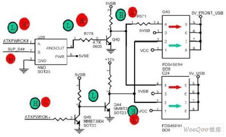
When it is working, ATXPWROK is high level. Q45 is connected and Q44 is disconnected. +12V voltage will be put on Q43 and Q24's pin 2 through resistors, that is binary channels MOS tube's N channel's control pin is high level and the channel is connected. At that time, VCC voltage will output 5V USB voltage from pin7,pin8 through N-type MOS tube. At the same time, when ATXPWROK is high level, ATXPWROK # is low level, then ANT GATE U26 outputs low level. Q40 is disconnected and will output high level control signal to Q43 and 24's pin 4, that is binary channel MOS tube's P-type channel is disconnected. Then pin 5, pin 6 have no output current, that is 5VSB doesn't supply 5VUSB voltage. (View)
View full Circuit Diagram | Comments | Reading(989)
Computer motherboard circuit 810 2_20
Published:2011/7/26 21:53:00 Author:Ecco | Keyword: Computer motherboard
View full Circuit Diagram | Comments | Reading(531)
Receiving Timing Signal Generation Circuit
Published:2011/7/19 8:06:00 Author:Sue | Keyword: Timing, Signal Generation
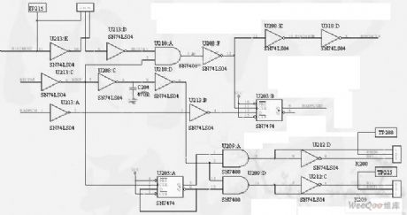
From the figure we can know that similar to transmitting timing signal, the way of timing signal generation is the same, so the waveform is omitted. What should be noted is that, the function of U213:A,B(74LS04), U203:B(74LS74) is to shape and output the received digital baseband signal.
The function of U213:D,E(74LS04), U210:A(74LS08), U208:D,E(74LS08) is to output received clock signal 1024KHz by using the received enable signal(generated by software). (View)
View full Circuit Diagram | Comments | Reading(742)
The automobile storage battery burglarproof alarm
Published:2011/7/22 21:06:00 Author:qqtang | Keyword: storage battery, burglarproof alarm
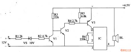
Here is to introduce the automobile storage battery burglarproof alarm, which can emitter signal when the output wire of the battery is cut off, it can be used in the burglarproof alarm of cars and motors.The working principle of the circuitThe automobile storage battery burglarproof alarm consists of the detection control circuit and alarm circuit, see as figure 7-112.
The detection circuit consists of the resistors R1-R5, regulated diode VS and transistors V1-V3.The alarm circuit consists of the audio integrated circuit IC, resistor R6 and loudspeaker BL. (View)
View full Circuit Diagram | Comments | Reading(614)
Infrared Remote Control Antitheft Coded Lock Circuit
Published:2011/7/16 6:40:00 Author:Sue | Keyword: Infrared, Remote Control, Antitheft, Coded Lock
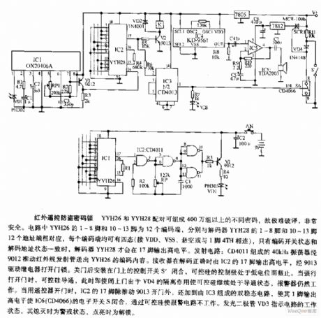
YYH26 and YYH28 can compose at least 4 million different groups of codes when these two are working in pairs. It is very different to decipher so it will be very safe. In the circuit, YYH26's pin 1-8 and pin 10-13 are 12 encoding terminals respectively which are corresponding to decoder YYH28's 12 address ports pin 1-8 and pin 10-13. Each encoding terminal can have 4 states(connect VDD,VSS,be suspend in air, or be connected to pin 1 4TH). Only when the encoding switch state is corresponding to the decoding address state, the decoder YYH28can output high level from pin 17. Emitting circuit: The 40kHz oscillator composed of CD4011 will output encoding content of YYH26 through 9012 push infrared ray transmitting tube. When encoding is correct, the receiver can output high level through IC2's pin 17 and unlock the lock by 9013 driven relay. When the door is closed, the control switch S' which is set on the door will be disconnected. Then the silicon control's control stage is disconnected because of low level. (View)
View full Circuit Diagram | Comments | Reading(542)
The public bus door shutting reminder
Published:2011/7/22 20:46:00 Author:qqtang | Keyword: public bus, door shutting reminder
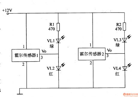
The working principle of the circuitThe public bus door shutting reminder consists of the +12V resistors of R1 and R2, LED VL1-VL4, Hall sensors of 1 and 2, see as figure 7-115.
Hall sensor 1 and Hall sensor 2 are installed on the door frames of the bus, and in the corresponding places, there is a magnetic steel chip on either door. (View)
View full Circuit Diagram | Comments | Reading(520)
The steering lamp shutting reminder
Published:2011/7/22 20:33:00 Author:qqtang | Keyword: steering lamp, shutting reminder
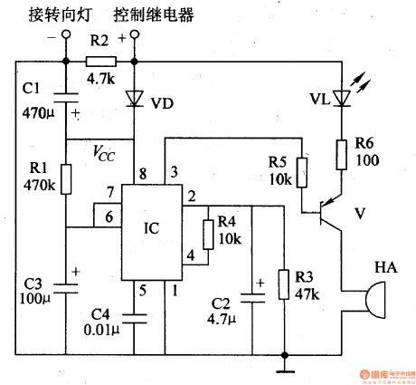
Here is to introduce the steering lamp shutting reminder made of the 555 time based integrated circuit, which can emit the alarm signal when the driver forgets to shut off the steering lamp, so the driver will shut the lamp.The working principle of the circuit The steering lamp shutting reminder consists of the time-based integrated circuit IC, transistor V, diode VD, LED VL, resistor R1-R6, capacitor C1-C4 and buzzer HA, see as figure 7-118.
(View)
View full Circuit Diagram | Comments | Reading(510)
The motor headlight shutting reminder
Published:2011/7/22 20:58:00 Author:qqtang | Keyword: headlight, shutting reminder
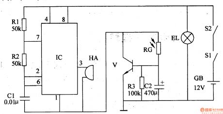
The working principle of the circuitThe motor headlight shutting reminder consists of the light control switch circuit and audio alarm circuit, see as figure 7-119.
The light control switch circuit consists of the light sensitive resistor RG, resistor R3, capacitor C2 and transistor V.The audio alarm circuit consists of the time-based integrated circuit IC, resistors of R1 and R2, capacitor C1 and buzzer HA.GB is the battery of the motor, S1 is the car lock switch, S2 is the headlight switch, EL is the headlight. (View)
View full Circuit Diagram | Comments | Reading(879)
School Bells Analog Circuit
Published:2011/7/16 7:15:00 Author:Sue | Keyword: School Bells, Analog
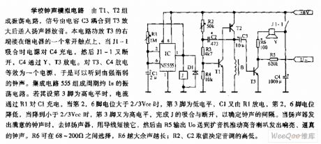
T1,T2 will compose oscillate circuit. The signal will be coupled to T3 through the capacitor C3, which will be sent to the loud speaker after the signal is amplified. The circuit's T3's right terminal is connected to a normally open contactor of the relay. When J1-1 is connected, the power will charge C4. Then J1-1 is disconnected, C4 will be discharged through Y,T3. Discharging T3,C4 will be equal to a power supply so a weakening bell will be heard. The integrated circuit 555 will compose oscillate circuit with a period of about 1s. If its pin 3 is high level, the current will charge C1 through R1. When the potential of pin2, 6 is higher than 2/3Vcc, pin 3 has low level. C1 will then be charged through R1, and potential of pin 2,6 will be lower. When it is lower than 2/3Vcc, pin 3 has high level again. By controlling J's connection and disconnection, the interval of the bell can be controlled. When the sound from the loud speaker is good, the loud speaker can be moved. Then use a wire to short, and R5 will output U0. U0 will be sent to the loud speaker to drive the high tone loud speaker to make a loud and vivid sound. R6 can choose from 68-200Ω. The larger R6 is, the longer the aftersound is. R2,C2 are decided by the tone. (View)
View full Circuit Diagram | Comments | Reading(623)
Computer motherboard circuit 810 2_22
Published:2011/7/26 21:55:00 Author:Ecco | Keyword: Computer motherboard
View full Circuit Diagram | Comments | Reading(551)
Computer motherboard circuit 810 2_21
Published:2011/7/26 21:54:00 Author:Ecco | Keyword: Computer motherboard
View full Circuit Diagram | Comments | Reading(554)
| Pages:1456/2234 At 2014411442144314441445144614471448144914501451145214531454145514561457145814591460Under 20 |
Circuit Categories
power supply circuit
Amplifier Circuit
Basic Circuit
LED and Light Circuit
Sensor Circuit
Signal Processing
Electrical Equipment Circuit
Control Circuit
Remote Control Circuit
A/D-D/A Converter Circuit
Audio Circuit
Measuring and Test Circuit
Communication Circuit
Computer-Related Circuit
555 Circuit
Automotive Circuit
Repairing Circuit