
Circuit Diagram
Index 1450
INVERTING_SUMMING_AMPLIFIER
Published:2009/6/15 2:38:00 Author:May
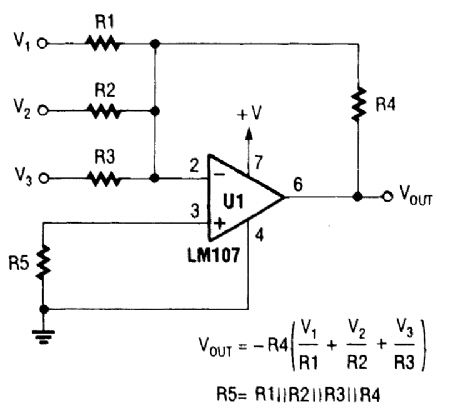
The out put of U1 is the sum of V1, V2, and V3, multiplied by R1/R4, R1/R4, and respectively. R1, R2, R3 are selected as required for individual gains. R4 affects gain of all these inputs. (View)
View full Circuit Diagram | Comments | Reading(1415)
FAST_INVERTING_AMPLIFIER_WITH_HIGH_INPUT_IMPEDANCE
Published:2009/6/15 2:27:00 Author:May
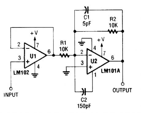
U1 is used as a voltage follower to feed in-verter U2. Because UI is in the voltage-follower configuration, it exhibits a high input impedance. (View)
View full Circuit Diagram | Comments | Reading(1278)
DIFFERENCE_AMPLIFIER
Published:2009/6/15 2:25:00 Author:May
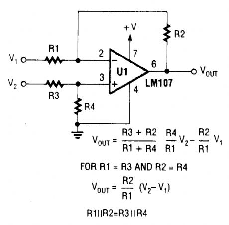
By using two inputs as shown, a difference amplifier yielding the differential between U1 and U2, times a gain factor results. (View)
View full Circuit Diagram | Comments | Reading(1584)
SILENT_ALARM
Published:2009/6/14 23:10:00 Author:May
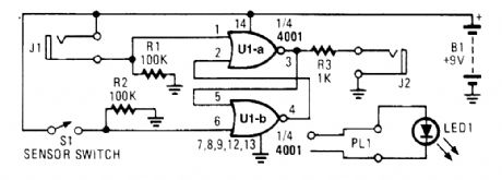
A sensor switch triggers a set-reset flip flop and lights an LED. (View)
View full Circuit Diagram | Comments | Reading(947)
BURGLAR_CHASER
Published:2009/6/14 23:07:00 Author:May
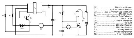
BZ..................... Mtai Horn Buzzer C1 ..............5μF 250 volts Capactto C2.............022μF Green Cap(223 K5K)D1..........................1N4O07 DiodeFT.......... Micro Strobe Tube/ReflectorL1.............................Neon Lamp Q1.................. C174O SW Transistor Q2...............................106 SOP R1......................200 ohm Resistor R2......................820 ohm Resistor R3.......................10 meg ReststorT1...................Invener TransformerT2.................... 4 kV Trtgger Coil
The burglar chaser makes a great accessory for any alarm system. It creates brilliant flashes of white light and a loud, irritating sound from a metal horn buzzer. Transformer T1 is connected to Q1, R1, and R2 to formablocking oscillator. This createsaG-Vac signal on the primary ofT1. Because of T1's large ratio of turns frorn primary to secondary, the 6-Vac signal is stepped up to a level of over 200 Vac, which is then rectified by D1. The resultant dc voltage is applied to storage capacitor C1 and the neon relaxation oscillator made up of R3, C2, and L1. Each time C2 charges up to a sufficient level, it ionizes L1, which causes SCR Q2 to fire. The firing SCR causes the charge on C2 to be applied to the trigger coil. The trigger coil converts the 200 V into the 4000-V pulse that is needed to fire micro xenon strobe tube/reflector FT. The cycle repeats itself after the strobe tube flashes. (View)
View full Circuit Diagram | Comments | Reading(1683)
ALARM_SOUNDER_FOR_FLEX_SWITCH
Published:2009/6/14 23:02:00 Author:May
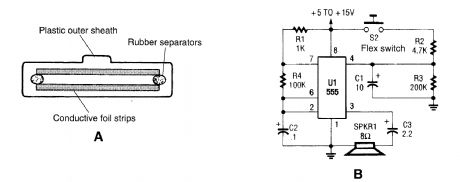
This is a cross-sectional diagram of a flex switch. They can be used as pushbutton or even posi-tion sensors. This schematic diagram shows an oscillator, which is used as an alarm sounder, trig-gered by a flex switch. (View)
View full Circuit Diagram | Comments | Reading(888)
SELF_LATCHING_LIGHT_ALARM_WITH_TONE_OUTPUT
Published:2009/6/14 23:00:00 Author:May
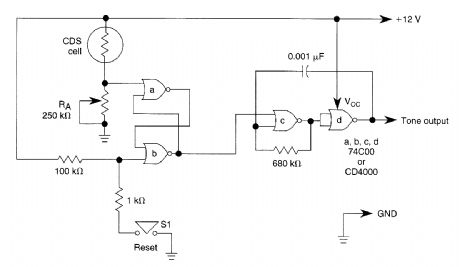
A decrease in the resistance of the CDS cell when light strikes it activates latch a and b, enabling Lone oscillator c and d which produces an output of about 1000 Hz. RA sets the trip level. S1 resets Lhe circuit. (View)
View full Circuit Diagram | Comments | Reading(925)
HIGH_OUTPUT_PULSED_TONE_LIGHT_ACTIVATED_ALARM
Published:2009/6/14 22:58:00 Author:May
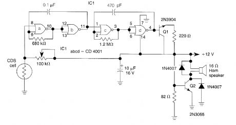
This circuit can produce up to 1 W of audio power to drive a speaker or horn. When the CDS cell is struck by light, its resistance decreases thus activating NOR gate(a) thereby causing(a) and(b) to produce a low-frequency(10-Hz) square wave. This pulses the 1-kHz oscillator(c) and(d), caus-ing it to generate a pulsed 1-kHz tone at a 10-Hz rate. Q1 and Q2 amplify this signal. Q2(2N3055) drives the speaker. (View)
View full Circuit Diagram | Comments | Reading(987)
PRECISION_LIGHT_ALARM_WITH_HYSTERESIS
Published:2009/6/14 22:57:00 Author:May
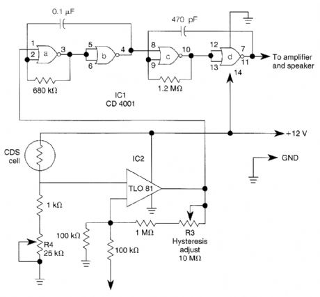
The TL081 is used as a comparator in a Wheatstone bridge circuit. When the CDS cell resistance decreases due to exposure to light, the output from IC2 cause the low-frequency osciLator(a) and(b) to generate a 10-Hz square wave, gating the 1000 Hz oscillator(c) and(d) on and off. This signal dri-ves an amplifier. R3 controls hysteresis, which reduces on-off triggering near the threshold set by R4. (View)
View full Circuit Diagram | Comments | Reading(1434)
PRECISION_LIGHT_ACTIVATED_ALARM
Published:2009/6/14 22:55:00 Author:May
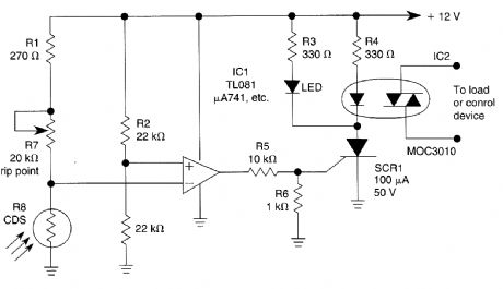
The light-sensitive CDS cell R8 conftgured In a bridge circuit with IC1 as a comparator causes IC1's output to go high when light strikes the CDS cell R8,triggering SCR1 This lights LED1 andturns on opto isolator IC2,which switches the load (View)
View full Circuit Diagram | Comments | Reading(1505)
LIGHT_ACTIVATED_ALARM_WITH_LATCH
Published:2009/6/14 22:55:00 Author:May
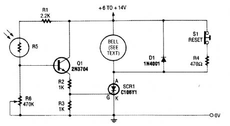
In this circuit, light causes R5 to conduct forward-biasing Q1. R6 sets sensitivity. SCR1 is triggered from the emitter voltage on LQ1, sounding the alarm bell. When 51 is depressed, SCR1 un-latches. Be sure that a self-interrupting alarm (electromechanical buzzer or bell) is used. (View)
View full Circuit Diagram | Comments | Reading(1177)
LIGHT_BEAM_ALARM_PREAMPLIFIER
Published:2009/6/14 22:53:00 Author:May
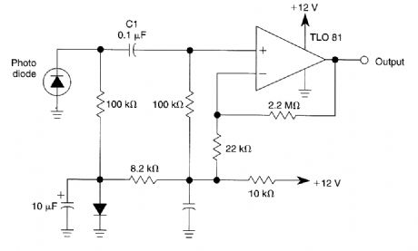
This circuit can be used for light beams to 20 kHz .The gain of the operational amplifier is set for a 40-dB gain. (View)
View full Circuit Diagram | Comments | Reading(1212)
DARK_ACTIVATED_ALARM_WITH_PULSED_TONE_OUTPUT
Published:2009/6/14 22:51:00 Author:May
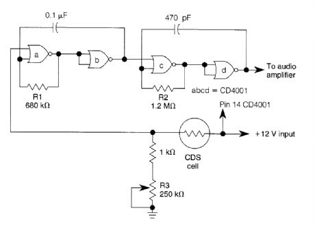
NOR gates a and b form a low-frequency oscillator that is activated when the CDS cell,underdark conditions,causes NOR gate ato see alogic zero at one input This low-frequency (10 Hz) gates a high-frequency oscillator (c and d) to oscillate at around 1000 Hz.R1 can be varied to change the pulse rate and R2 to change the tone.R3 sets the trigger point. (View)
View full Circuit Diagram | Comments | Reading(1823)
LIGHT_BEAM_ALARM_FOR_INTRUSION_DETECTION
Published:2009/6/14 22:46:00 Author:May
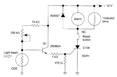
When the light beam that falls in the CDSphotocell is interrupted,transistor(EN3904) conducts thereby triggering SCR1 (C106) and activating alarm bell. S1 resets the SCR. The alarm bell should be a self-interrupttng electromechanical type. (View)
View full Circuit Diagram | Comments | Reading(2148)
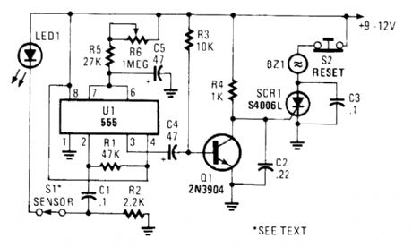
555_BASED_ALARM
Published:2009/6/14 22:43:00 Author:May
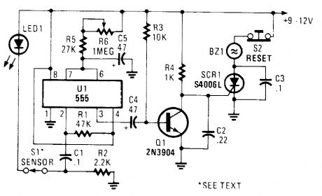

The alarm circuit has a single 555。scillator/timer(U1)performing double duty;serving both in the alarm-trigger circuit and the entry-delay circuit. In this application,the trigger mput of U1 at ptn 2 iS held high via R1,A normally-closed sensor switch,S1,supplies a positive voltage to the junction of R2 and C1,and lights LED1.With both ends of C1 tied high,there is no charge on C1 But when S1 opens,C1(initially acting as a short) momentarny pulls pm 2 of U1 low, triggering the timed delay circle At the beginning of the timing cycle,U1 produces a positive voltage at put 3,which charges FAUito near the positive voltage at put 3,which charges C4 to near the positive supply voltage Transistor Q1 is heavily biased on by R3,keeping its collector at near ground level With Qt on,SCR1’s gate lOclamped to ground,holding it off. When the delay circuit times out,pin 3 of U1 goes low and ties thepositive end of C4 to ground,That turns Q1 offWhen Q1 turns off,the voltage at the gate of SCR goes positive,turning on the SOP and sounding the alarm,The delay time is adjustable from just a few seconds(R6 set to its minimum resistance) to about one minute(R6 adjusted to its maximum resistance) (View)
View full Circuit Diagram | Comments | Reading(1087)
THERMOSTAT_SWITCH_FOR_AUTOMOTIVE_ELECTRIC_FANS
Published:2009/6/14 22:25:00 Author:May
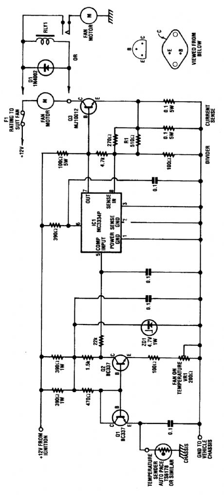
The circuit is based on a commercial temperature sensor(TS6178) and an MC3334P ignition chip. When the radiator temperature increaser,the sensor pulls the base of Q2 low via Q1, which is wired as a diode.Q2's collector thus goes high and riggers IC1,which switches its pin 7 output high and turns on the fan motor via Q3. (View)
View full Circuit Diagram | Comments | Reading(1538)
EXIT_DELAY_FOR_BURGLAR_ALARMS
Published:2009/6/14 22:16:00 Author:May
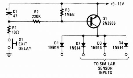
Depressing S1 charges C1 to the supply voltage. This biases Q1 on via bias resistors R2 and R3. A voltage is available for the duration of the delay period, to hold off the alarm circuit.C1 can be increased or decreased in value to al-ter the delay times. (View)
View full Circuit Diagram | Comments | Reading(1088)
PIEZOELECTRIC_ALARM
Published:2009/6/14 22:13:00 Author:May
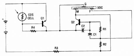
01,C2...............047 Disc Capacitor Q1,Q2.......... ... 2N3906 Transistor R1................ 6.8K Resistor R2..................33K Resistor R3................. 200 ohm Resistor R4..................75K Resistor XDC.................Piezoelectric transducer
The alarm uses a fixed-frequency piezoelectric buzzer in conjunction with the cadmium-sulfide (CDS) cell and the two-transistor circuit to provide a unique effect. Whenever light reaches the CDS photo-electric cell, the alarm is silent. But when no light strikes the cell, transistor Q1 tums on, and the circuit emits a high-pitched tone.The alarm consists of a piezoelectric disk that oscillates at the fixed frequency of 3. 137 kHz, cre-ated by transistor Q2, capacitor C1 and C2, and resistors R1 through R3. Transistor Q1 is used as a switch. It is forward-biased on by R4; however, the CDS cell turns Q1 off when the light is strik-ing it.A CDS photo cell is made from cadmium sulfide, a semiconductor material that changes resis-tance when the light strikes it. The greater the amount of light, the lower the resistance. The low re-sistance conducts positive voltage to the base of pnp transistor Q1, keeping it turned off' when the light shines on the CDS cell. As soon as the light is removed, the CDS cell provides a resistance of over 100 kQ. That causes Q1 to tum on, allowing a positive voltage to reach the emitter lead of Q2, which then begins to oscillate. That then causes the piezoelectric element (transducer) to produce a loud signal. (View)
View full Circuit Diagram | Comments | Reading(1316)
HEAT_OR_LIGHT_ACTIVATED_ALARM
Published:2009/6/14 22:06:00 Author:May
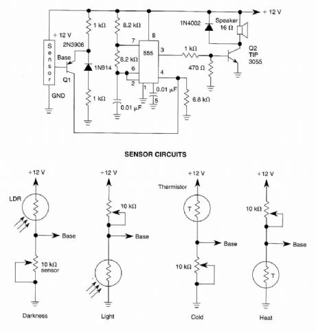
The tone generated by a 555 oscillator can be turned on (activated) by heat or light. That causes Q1 to conduct transistor W2 (TIP 3055).Q2 (TIP 3055) acts as an audio amplifier and speaker driver. (View)
View full Circuit Diagram | Comments | Reading(1774)
NO_DOZE_ALARM
Published:2009/6/14 22:00:00 Author:May
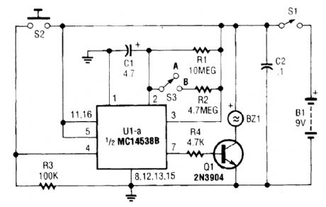
This circuit sends out a loud tone if the input switch(S2) is not retriggered at pre-set intervals. If you fall asleep and miss re-triggering the circuit, it will sound until you press S2. (View)
View full Circuit Diagram | Comments | Reading(920)
| Pages:1450/2234 At 2014411442144314441445144614471448144914501451145214531454145514561457145814591460Under 20 |
Circuit Categories
power supply circuit
Amplifier Circuit
Basic Circuit
LED and Light Circuit
Sensor Circuit
Signal Processing
Electrical Equipment Circuit
Control Circuit
Remote Control Circuit
A/D-D/A Converter Circuit
Audio Circuit
Measuring and Test Circuit
Communication Circuit
Computer-Related Circuit
555 Circuit
Automotive Circuit
Repairing Circuit