
Circuit Diagram
Index 1446
MINI_AMPLIFIER_USING_LM1895N
Published:2009/6/15 22:58:00 Author:May
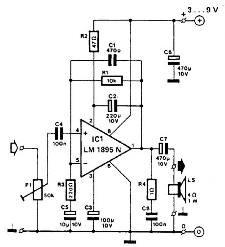
With 3-V to 9-V supplies, this amplifier can provide from 100-mW to 1-W output into a 4 Ω and bandwidth is approximately 20 kHz @ 3 dB.This circuit is useful for low-power and battery applications. Drain is 80 mA @ 3 V or 270 mA @ 9 V at maximum signal conditions. (View)
View full Circuit Diagram | Comments | Reading(760)
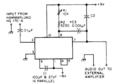
455_kHz_FM_DEMODULATOR
Published:2009/6/15 22:57:00 Author:May
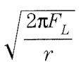
Free-running frequency of VCO:fos=1.2/4(R1)(C1) lock range f1=±8fos/VCC capture rang fc=±1/2π where r=(3.6×10³)(C2)
Useful for NBFM reception on older shortwave receivers lacking this capability,this circuit uses a PLL IC,an N565N,to achieve this.It was originally used with an old Hammarlund HQ-170 receiver, for both 6-and 10-m FM reception. (View)
View full Circuit Diagram | Comments | Reading(996)
CONSTANT_VOLUME_AMPLIFIER
Published:2009/6/15 22:57:00 Author:May
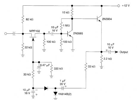
The amplifier has an output level that shifts about 6 dB for a 40-dB input variation. (View)
View full Circuit Diagram | Comments | Reading(809)
LOW_DRIFT_PEAK_DETECTOR
Published:2009/6/15 22:55:00 Author:May
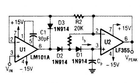
Leakage of D2 is provided by feedback path throtlgh Rf Leakage of circuit is essenttany lb(LF155,LF156) plus capacitor leakage of Cp Diode D3 clamps Vout (Al) to Vin-VD3 to improve speed and to limit reverse bias of D2 Maximum input frequency should be<<1/2πRfCD2,where CD2 is shunt capacitance of D2 (View)
View full Circuit Diagram | Comments | Reading(3015)
AUDIO_LINE_DRIVER
Published:2009/6/15 22:50:00 Author:May
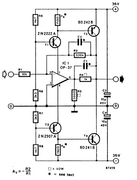
This line driver can drive low-impedance lines with up to 70 V p-p max. IC1 is a low-noise op amp suitable for ±15-V operation. T1 and T2 are regulators for the power supply for IC1. T3 and T4 form a complementary power output stage. Frequency response is flat up to 100 kHz. (View)
View full Circuit Diagram | Comments | Reading(1091)
HEADPHONE_AMPLIFIER
Published:2009/6/15 22:48:00 Author:May
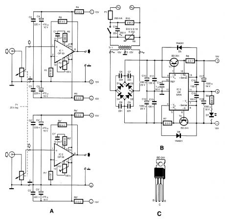
Built around Precision Monolithics Inc. OP-50 op amps,this amplifier will drive 100-Ω to 1-kΩ headphone,is flat within 0.4 dB from 10 Hz to 20 kHz,and has a THD of less than 0.01% over most of the audio range. Amplification factor is about 6X. (View)
View full Circuit Diagram | Comments | Reading(2542)
NEGATIVE_PEAK_DETECTOR
Published:2009/6/15 22:39:00 Author:May
View full Circuit Diagram | Comments | Reading(1)
AIR_FLOW_DETECTOR
Published:2009/6/15 22:39:00 Author:May
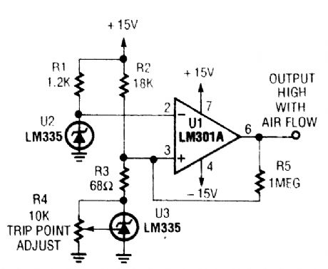
Two precision temperature sensors are used to detect a small temperature difference. When air flow occurs, self-heating of the LM335 is re-duced, and the output of the two temperature sensors is unequal. This is amplified by U1. (View)
View full Circuit Diagram | Comments | Reading(3339)
FAST_PULSE_DETECTOR
Published:2009/6/15 22:37:00 Author:May
A fast pulse detector can be made with this circuit. A very fast input pulse will exceed the am-plifier slew rate and cause a long overload recovery time. Some amount of dv/dt limiting on the input can help this overload condition, however this will delay the response. (View)
View full Circuit Diagram | Comments | Reading(883)
CLOSED_LOOP_PEAK_DETECTOR
Published:2009/6/15 22:33:00 Author:May
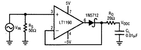
This closed-loop peak detector circuit uses a Schottky diode inside feedback loop to obtain good accuracy. The 20-Ω resistance R, isolates the 0.01-μF load and prevents oscillation. The dc value is read with a DVM. At a low frequency, the error is small and dominated by the decay of the detector capacitor between cycles. As the frequency rises, the error increases because capacitor charging time decreases. During this time, the overdrive becomes a very small portion of a sine-wave cycle. Finally, at approximately 4 MHz, the error rises rapidly because of the slew-rate lim-itation of the op amp. (View)
View full Circuit Diagram | Comments | Reading(2505)
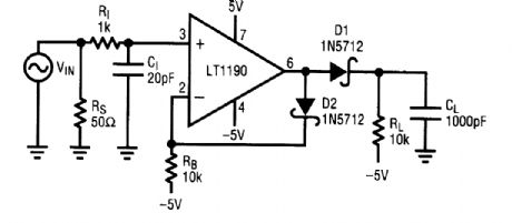
OPEN_LOOP_PEAK_DETECTOR
Published:2009/6/15 22:33:00 Author:May
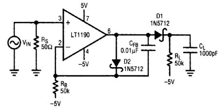
In this open-loop design, the detector diode is D1, and a level shifting or compensating diode is D2. Load reststor RL is connected to -5V, and an identical bias resistor RL is connected to -5 V, and identical bias resistor RL is used to bias the compensating diode. Resistors with equal values ensure that the diode drops are equal. Low values of RL and RB (1kΩ to 10kΩ) provide fast response, but at the expense of poor low-frequency accuracy. High values of RL and RB provide good low-frequency accuracy, but cause the amplifier to slew rate limit, resulting in poor high-frequency accuracy. A good compromise can be made by adding a feedback capacitor CFB which enhances the negative slew rate on the (-) input. (View)
View full Circuit Diagram | Comments | Reading(755)
FAST_HIGH_VOLTAGE_LINEAR_POWER_AMP
Published:2009/6/15 22:32:00 Author:May
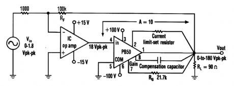
An Apex PB50 Booster Amplifier,plus an IC op amp,can be used In a high-voltage op amp thatconverts a small analog signal to a 180-V p-p signal. (View)
View full Circuit Diagram | Comments | Reading(881)
AUDIO_POWER_AMPLIFIER
Published:2009/6/15 22:31:00 Author:May
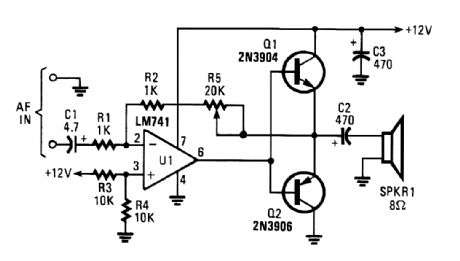
The circuit, built around an LM741 op amp configured as an inverting amplifier, is used to drive complementary transistors (Q1 and Q2). The op amp's feedback loop includes the base-emitter junctions of both transistors-an arrangement that helps to reduce crossover distortion that would normally occur as a result of the emitter-to-base junction voltage drop of about 0.6 V. Potentiometer R5 varies the amplifier's voltage gain from 1 to about 20. As much as 0.5 TV can be obtained from the circuit if a heatsink is added to the transistors. (View)
View full Circuit Diagram | Comments | Reading(9617)
SIMPLE_FULL_WAVE_ENVELOPE_DETECTOR
Published:2009/6/15 22:26:00 Author:May
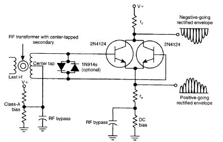
Simple, yet sensitive, this amplifying full-wave detector circuit has an almost zero rectification threshold. It presents a highly linear RF load to the final IF stage. The gain for the collector output is given (approximately) by rc/re, The emitter output gain is slightly less than unity. (View)
View full Circuit Diagram | Comments | Reading(1102)
SUBWOOFER_CROSSOVER_AMPLIFIER
Published:2009/6/15 22:26:00 Author:May
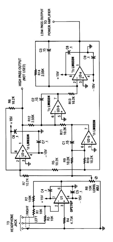
The electronic-crossover circuit contains a summing ampplifier that combines the left that combines the left and right channels from a stereo's headphone jack. Originally used in a subwoofer system, the above circuit might be useful in similar audio applications. (View)
View full Circuit Diagram | Comments | Reading(1388)
555_MISSING_PULSE_DETECTOR
Published:2009/6/15 22:26:00 Author:May
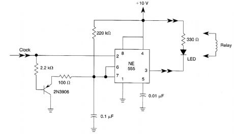
This missing pulse detector can use an LED or relay output. (View)
View full Circuit Diagram | Comments | Reading(2466)
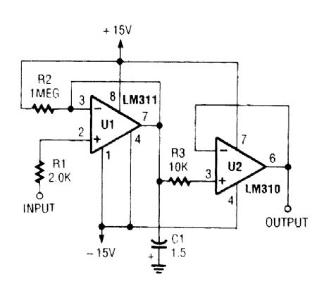
FM_DEMODULATOR
Published:2009/6/15 22:23:00 Author:May
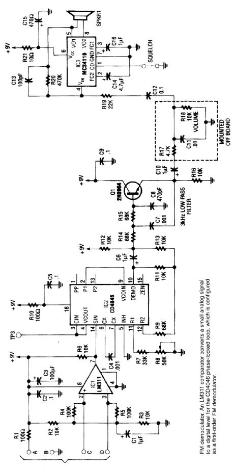
An LM311 comparator converts a small analog signal to a digital level for the DC4046 phase-locked loop, which is config-ured as a first-order FM demodulator. This demodulator works with a 50-kHz FM modulated input signal. It has applications in FM light beam receivers or in remote control applications. Pin 1 of IC3 can be used to squelch the receiver if it is lifted from ground if not desired, leave it grounded. (View)
View full Circuit Diagram | Comments | Reading(3)
18_W_BRIDGE_AUDIO_AMPLIFIER
Published:2009/6/15 22:18:00 Author:May
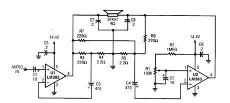
Two LM383 IC devices are used in a bridge circuit that is useful for auto sound applications. (View)
View full Circuit Diagram | Comments | Reading(1948)
SUBWOOFER_AMPLIFIER
Published:2009/6/15 22:17:00 Author:May
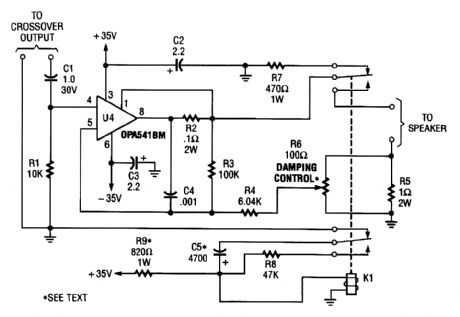
Designed to feed a low-frequency subwoofer speaker system,the amplifier is capable of up to 100 W into an 8-Ω load. The OPA541BM op amp requires heatsinkins and is manufactured by Burr-Brown Corporation. A damping control and a relay to eliminate turn-on and turn-off thump in the speaker is included. (View)
View full Circuit Diagram | Comments | Reading(2021)
BUG_DETECTOR
Published:2009/6/15 22:16:00 Author:May
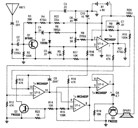


The circuit, built around a single integrated circuit (U1, an MC3403P quad op amp), three tran-sistors (Q1-Q3), and a few support components, receives its input from the antenna (ANTI). The signal is fed through a high-pass filter, formed by C1, C2, and RI, which eliminates bothersome 60-Hz pickup from any nearby power lines or line cords located in and around buildings and homes.From the high-pass filter, the signal is applied to transistor Q1 (which prov'tdes a 10-dB gain for frequencies in the 1- to 2000-MHz range) for amplification. Resistors R2, R3, and R4 form the biasing network for Q1. The amplified signal is then ac coupled, via capacitor C4 and resistor R7's (the sensi-tivity control) wiper, to the inverting input (pin 2) of U1-a. Op amp U1-a is configured as a very high gain amplifier. With no signal input from ANTI, the output of U1-a at pin 1 is near ground potential.When a signal from the antenna is applied to the base of Q1, it turns on, producing a negative-go-ing voltage at the cathode of Dl. That voltage is applied to pin 1 of UI-a, which amplifies and inverts the signal, producing a positive-going output at pin 1. Op amps UI-b and UI-c along with CS, RIO through R18, and Q2 are arranged to form a voltage-controlled oscillator fi/CO) that operates over the audio-frequency range. As the output of U1-a increases, the frequency of the VC0 increases. The VCO output, at pin 8 of U1-c, is fed to the input of U1-d, which is configured as a noninverting, unity-gain (buffer) amplifier. The output of U1-d is used to drive Q3, which, in turn, drives the output speaker. (View)
View full Circuit Diagram | Comments | Reading(3277)
| Pages:1446/2234 At 2014411442144314441445144614471448144914501451145214531454145514561457145814591460Under 20 |
Circuit Categories
power supply circuit
Amplifier Circuit
Basic Circuit
LED and Light Circuit
Sensor Circuit
Signal Processing
Electrical Equipment Circuit
Control Circuit
Remote Control Circuit
A/D-D/A Converter Circuit
Audio Circuit
Measuring and Test Circuit
Communication Circuit
Computer-Related Circuit
555 Circuit
Automotive Circuit
Repairing Circuit