
Circuit Diagram
Index 1445
AGC_SYSTEM_FOR_AUDIO_SIGNALS
Published:2009/6/15 23:32:00 Author:May
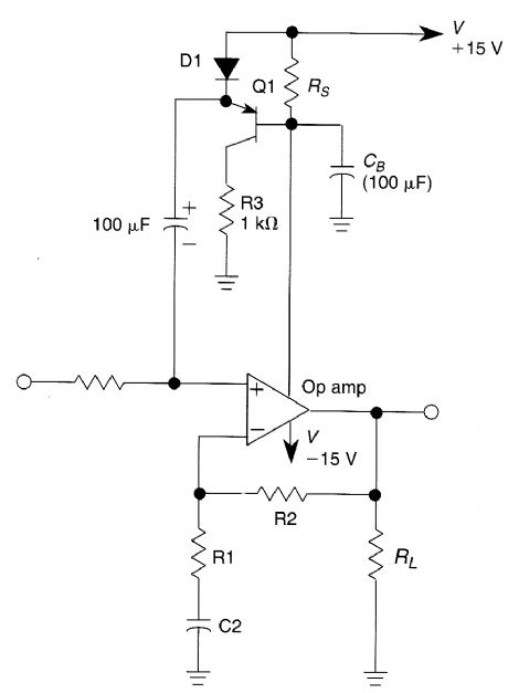
This circuit is an AGC system for audio-fre-quency signals. AGC systems usually consist of three parts: an amplifier, rectifier, and controlled impedance. In this circuit the functions of an ampltfier and a rectifier are performed by a single op amp. This makes the system simple and cheap.The rectifier is made with the output push-pull cascade of the op amp and RS, RL, and CB. The transistor Q1 and D1 are used as a voltage-controlled resistance (Z). The input signal is (Z + R1)/Z times, diminished by the voltage divider and 1 + R2/R1 times, amplified by the op amp. C2 eliminates influence of dc bias voltage. R3 protects Q1 and D1 from excessive current. (View)
View full Circuit Diagram | Comments | Reading(2295)
LARGE_LCD_DISPLAY_BUFFERING_DRIVER
Published:2009/6/15 23:30:00 Author:May
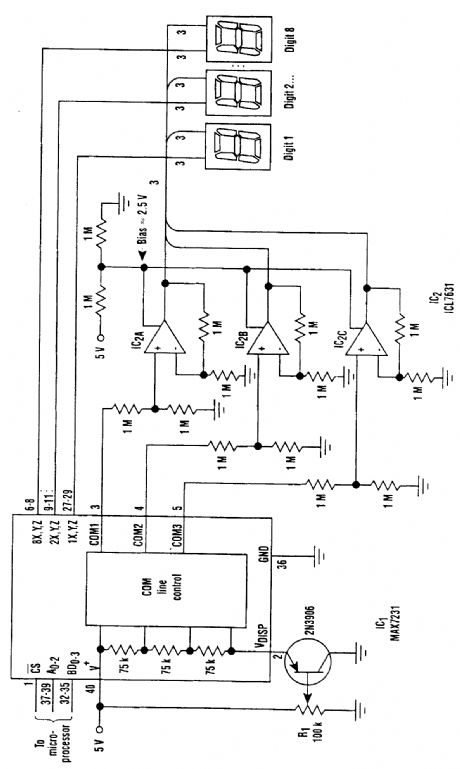
Large LCD devices of 1 or more exhibit a large driving capacitance to the driver circuits. To solve this problem, the drive cir-cuit shown (see the figure) introduces a buffer amplifier for each of the three common lines. Each amplifier can be programmed independently for a quiescent current of 10, 100, or 1000μA. In this application, the bias network applies a voltage that sets the three quiescent currents to 100μA.The display driver and triple op amp operate between 5 V and ground, and the COM signals range from 5 V to ≈1 V. To en-sure that these signals remain within the amplifiers' common-mode range, the signals are attenuated by one-half and the buffers operate at a gain of two. The circuit drives eight 1-inch displays, and is suitable for ambient temperature variations of 15°F or Iess.At the highest expected temperature, R1 should be adjusted so that no off segments are visible. (View)
View full Circuit Diagram | Comments | Reading(868)
NONINVERTING_ac_AMPLIFIER
Published:2009/6/15 2:32:00 Author:May
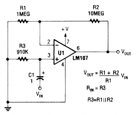
A general-purpose noninverting ac amplifier for audio of other low-frequency applications is shown. Design equations are in the figure. Almost any general-purpose op amp can be used for U1. (View)
View full Circuit Diagram | Comments | Reading(671)
DIGITAL_AUTOMATIC_LEVEL_COMTROLALC
Published:2009/6/15 23:26:00 Author:May


This approach to automatic level control(ALC) make use of digitally seitched audio attenuators in the signal path. The out-put level of the system is sensed, compared to a reference, and audio pads are inserted via analog switches. This method is nearly instantaneous and eliminates the compromises necessary in conventional RC network ALC systems useing fast attack,slow-decay approaches. (View)
View full Circuit Diagram | Comments | Reading(1220)
CASCADED_4026B_COUNTER_DISPLAY_DRIVER_CIRCUIT
Published:2009/6/15 23:21:00 Author:May
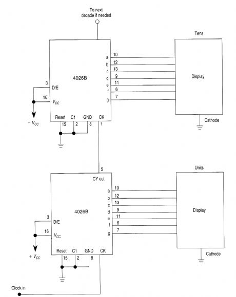
CASCADED 4026B COUNTER/DISPLAY DRIVER CIRCUIT (View)
View full Circuit Diagram | Comments | Reading(2437)
4033_DISPLAY_CIRCUITRY_COMMON_CATHODE
Published:2009/6/15 23:15:00 Author:May
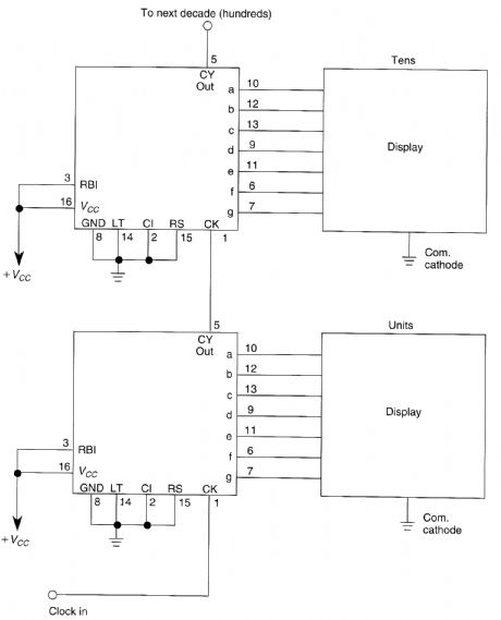
TO drive two or more common-cathode displays two or more 4033 decode counters can be cascaded (View)
View full Circuit Diagram | Comments | Reading(812)
AUDIO_DISTRIBUTION_AMPLIFIER
Published:2009/6/15 23:13:00 Author:May
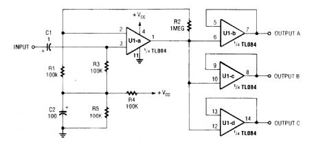
Three low-Z audio outputs are available from this circuit, using a quad TL084 FET amplifier. The input is high impedance. VCC can be 6 to 12 V for typical applications. (View)
View full Circuit Diagram | Comments | Reading(6624)
AUDIO_VOLUME_LIMITER
Published:2009/6/15 23:12:00 Author:May
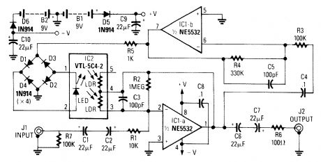
IC1-a is connected as an inverting amplifier whose gain is controlled by the LDR portion of an op-tocoupler. (View)
View full Circuit Diagram | Comments | Reading(2330)
BCD_ROTARY_SWITCH
Published:2009/6/15 23:11:00 Author:May
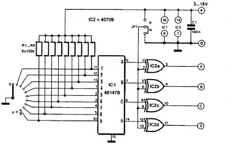
This circuit allows a simple rotary switch to emulate a BCD switch. The circuit draws about 200 mA. A 10-position rotary switch is used. (View)
View full Circuit Diagram | Comments | Reading(5016)
DIGITAL_CAPACITANCE_CONTROL
Published:2009/6/15 23:09:00 Author:May
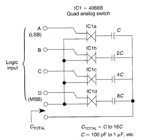
Digital capacitance control is possible with bilateral switches. Do not forget to consider ON resistance of the analog switches. (View)
View full Circuit Diagram | Comments | Reading(668)
AUDIO_BOOSTER
Published:2009/6/15 23:09:00 Author:May
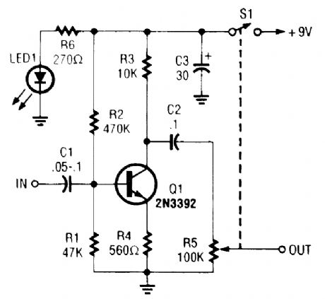
This circuit has a maximurn gain of about 22 dB (voltage gain), and it can be used for miscel-laneous audio circuits. (View)
View full Circuit Diagram | Comments | Reading(1674)
DIGITAL_RESISTANCE_CONTROL
Published:2009/6/15 23:09:00 Author:May

Digital resistance control is possible with bilateral switches. Do not forget that analog switches have on resistance. (View)
View full Circuit Diagram | Comments | Reading(1112)
MAGNETIC_PICKUP_PHONO_AMPLIFIER
Published:2009/6/15 23:07:00 Author:May
This preamp is RAA compensated for use with magnetic phone cartridges. (View)
View full Circuit Diagram | Comments | Reading(1895)
DUAL_PREAMP
Published:2009/6/15 23:06:00 Author:May

If you wish to amplify low-levle signals,such as the output of a turntable, the signal must first be fed to this preamp. (View)
View full Circuit Diagram | Comments | Reading(1104)
DIGITAL_MULTIPLE_GANG_POTENTIOMETER_CONTROL
Published:2009/6/15 23:06:00 Author:May
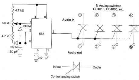
A 555 timer can be configured to simulate a multi-gang potentiometer by controlling the markspace ratio. The switching rate should be at least twice the maximum expected signal frequency the potentiometer has to handle. (View)
View full Circuit Diagram | Comments | Reading(752)
DIGITAL_AUDIO_SELECTOR
Published:2009/6/15 23:05:00 Author:May
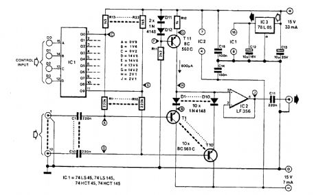
This circuit uses switched emitter followers, rather than the usual analog switch CMOS chips. This yields better reduction of crosstalk between channels. This circuit can handle up to 4 Vrms with less than -80-dB crosstalk. (View)
View full Circuit Diagram | Comments | Reading(1527)
JFET_HEADPHONE_AMPLIFIER
Published:2009/6/15 23:03:00 Author:May
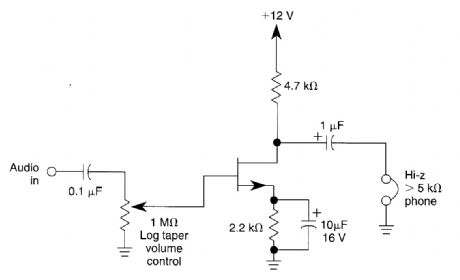
This circuit can drive high-impedance headphones from a low impedance low-level source. Gain is about 5X to 10X depending on headphone irnpedance. A volume control is included. (View)
View full Circuit Diagram | Comments | Reading(1497)
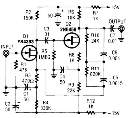
AUDIO_COMPRESSOR
Published:2009/6/15 23:02:00 Author:May
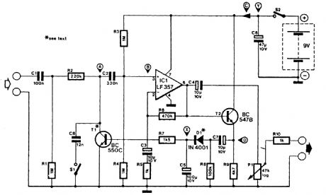
This compressor will compress a 25-mV p-p to 20-V p-p audio output to input levels remaining between 1.5Vp-p to 3.5 V p-p, and has a frequency response of 7 Hz to 67 kHz. It is suitable for audio and communications applications. (View)
View full Circuit Diagram | Comments | Reading(4)
AUDIO_AMPLIFIER_WITH_TUNEABLE_FILTER
Published:2009/6/15 23:00:00 Author:May
This audio amplifier can tune from 500 to 1500 Hz and will drive a speaker or headphones. Use-ful for CW reception or other receiver applications, only two IC devices are needed. (View)
View full Circuit Diagram | Comments | Reading(771)
DIGITAL_ENTRY_LOCk
Published:2009/6/15 23:00:00 Author:May

A block pinout diagram of the LS7220 keyless-lock IC is shown. The keypad must provide each key with a contact to a common connection. In this case, the common connection goes to the posi-tive supply rail so that when a key is pressed, a positive voltage is passed through to the wire associ-ated with that key. Each of the 12 keys are brought out to separate wires, and each wire is connected to a different pin of a 24-pin socket (SO1).To activate (unlock) the circuit, a preprogrammed four-digit access code must be entered in the proper sequence. The four-digit access code must be entered in the proper sequence. The four-digit access is programmed into the' circuit by connecting jumpers between terrrtinals of a 24-pin plug-in header.When the correct access code is entered (in the proper sequence), positive voltages appear at pins 3, 4, 5, and 6 of U1. That causes U1 to output a positive voltage at pin 13, which is fed through resistor R2 to the base of Q1, causing it to conduct. With Q1 conducting, its collector is pulled to ground potential, energizing relay K1. The normally open relay contacts close, switching on any ex-ternal device.Capacitor C2 controls the total time that the output of U1 at pin 13 is positive after the release of the first key. With avalue of 3.3 pF for C2, active time after release of the first key is about two sec-onds, assuming a 6-V supply or four seconds with a 12-V supply. Therefore, if you push the subse-quent keys too slowly, the relay might not close at all! To increase the time allotted for code entry, you will have to increase the capacitance of C2. (View)
View full Circuit Diagram | Comments | Reading(2)
| Pages:1445/2234 At 2014411442144314441445144614471448144914501451145214531454145514561457145814591460Under 20 |
Circuit Categories
power supply circuit
Amplifier Circuit
Basic Circuit
LED and Light Circuit
Sensor Circuit
Signal Processing
Electrical Equipment Circuit
Control Circuit
Remote Control Circuit
A/D-D/A Converter Circuit
Audio Circuit
Measuring and Test Circuit
Communication Circuit
Computer-Related Circuit
555 Circuit
Automotive Circuit
Repairing Circuit