
Circuit Diagram
Index 1452
Cable radio and amplifier protector circuit diagram
Published:2011/5/16 4:07:00 Author:Rebekka | Keyword: Cable radio , amplifier protector
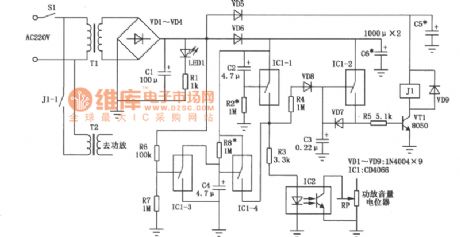
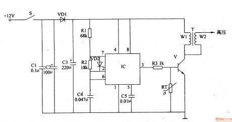
The high-power amplifiers radio used in the broadcast room of cable radio towns in rural areas is easily damaged. The reasons are: The frequent use, non-service management, the radio is often shut down when it works in the maximum volume state or the radio is started in the whole input power. This kind of amplifiers radio is arge output transformer output. There are are many transformers in the circuit. The peak inverse voltage maybe breakdown amplifier tube when you turn on or turn off the machine. The peak inverse voltage is caused by improper operation. The circuit can turn off the signal before the amplifier start to work. And it can also turn down the volume before the machine is turned off. So that the amplifier can be protected from damage. (View)
View full Circuit Diagram | Comments | Reading(721)
LCD projector multi-function controller circuit diagram
Published:2011/6/23 22:59:00 Author:Rebekka | Keyword: LCD projector multi-function controller
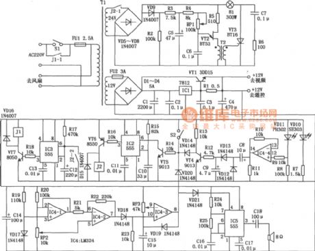
In the production of LCD projector, the main factors of the threatening life of LCD screen is the temperature of halogen. The multi-function controller made by this circuit is very effective for the protection of liquid crystal projector. The LCD projector multi-function controller circuit is shown as below. The circuit composed of VD1 ~ VD4, ICl, C1, VTl and other components provides a guarantee for the whole machine. The integral soft-start bulb circuit is composed of the VD5 VD8, C5, VT2, VT3 and other components. (View)
View full Circuit Diagram | Comments | Reading(5327)
Switching gain amplifier circuit composed of the INA115
Published:2011/6/27 4:20:00 Author:Rebekka | Keyword: Switching gain amplifier
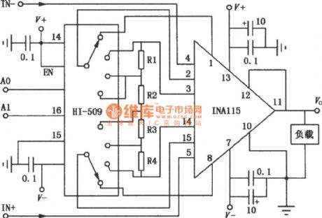
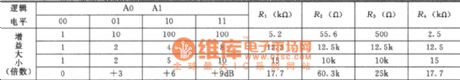
Switching gain amplifier circuit composed of the INA115 provides a different gain, it is shown as above. The lNA115 is a low cost general instrumentation amplifier, the circuit does not require external imbalance . It can be obtained a very high accuracy. The switching gain amplifier circuit composed of the HI-509 and INA115. R1 ~ R4 are gain resistances. It selects and calculates different gain resistors. You can gain access to different gear sizes. The formula is: A = 1 +50 kΩ / RG, A is the gain, RG is the gain resistor.
(View)
View full Circuit Diagram | Comments | Reading(743)
5V 2A PC standby power supply circuit composed of TNY255P
Published:2011/5/16 4:59:00 Author:Rebekka | Keyword: PC standby power supply
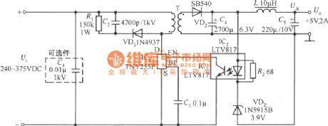
A 5V, 2A PC standby power supply circuit composed of TNY255P for PC is shown as above. Its input voltage Ui uses PC main power supply. The snubber circuit is composed of Rl, C2 and VDl. It can limit the spike voltage produced by TNY255P drain off mode in the safe range. The switching frequency of TNY255P is 130kHz. It is 3 times of TNY253P. So EE16 core can meet the standard of the 10W power output. The secondary voltage passes the VD2, C4, L and C5 rectifier filter and gains +5 V regulator output. (View)
View full Circuit Diagram | Comments | Reading(3336)
Sensitive signal amplifier circuit composed of F033
Published:2011/5/16 9:37:00 Author:Rebekka | Keyword: Sensitive signal amplifier
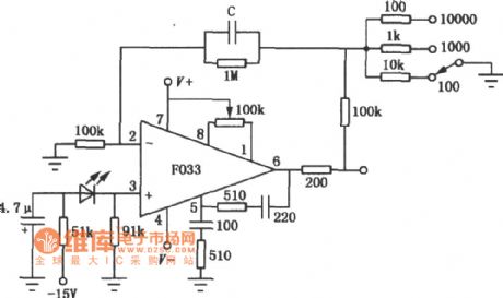
When the incident light illumination changes, it will generate a certain current on optical device. Because the photosensitive signal is very weak, it is better to choose the operational amplifier which has a low input bias current. The sensitive signal amplification circuit composed of the op amp F033 is shown as above. In order to eliminate oscillations, parallel connecting a small capacitor C (pF orders of magnitude) in the feedback circuit. The value of C has a influence on the bandwidth of the amplifier. The DC gain of the circuit is l00, 1000,10000. You can use gain to choose switch and make the corresponding 10kΩ, 1kΩ, 100Ω resistor connect to the ground to achieve. The resistor accuracy of the circuit must be better than ± 1%. The phototube uses FPT102 or FPT100. (View)
View full Circuit Diagram | Comments | Reading(575)
LM324 Single dual power general-purpose quad op amp circuit diagram
Published:2011/5/16 8:32:00 Author:Rebekka | Keyword: Single dual power, general-purpose quad op amp
LM324 is a high-gain op amp contains four units. Its features are: It can both work in single-supply and dual-supply. And it also can work in a wide supply voltage range. And the supply current is small. The input bias current is with temperature compensation. It's not need external frequency compensation components. LM324 can be used for convert amplifier, the DC gain unit and general-purpose op amp application circuits. It can be also used for a variety of logic circuits and other low-pressure system interface circuits. The similar or direct substitution models are: LMl24, CFl24MD, CF224LD, CFl24MJ, CF224LJ, CF324CJ, CF324CP and so on. The LM324 double-threshold voltage comparator circuit is shown as above. (View)
View full Circuit Diagram | Comments | Reading(4811)
μA747 dual power universal dual op amp circuit diagram
Published:2011/5/15 6:25:00 Author:Rebekka | Keyword: dual power universal, dual op amp
μA747 is a high gain dual op amp. The two op amps have a common bias and the negative power leads lines respectively. They have their independent functions in working mode. Its characteristics are: No external frequency compensation. It has a short-circuit protection, a wide differential mode a common mode input voltage range, low power consumption. It will not be blocked in the working mode. It can be used as integrator, summing amplifier and general feedback amplifier. The similar or direct substitution models are: CF747MT, CF747CT, CF747MD, CF747CD, CF747MJ, CF747CJ, CF747CP, SG747 and so on. The typical application circuit is shown as above. (View)
View full Circuit Diagram | Comments | Reading(1155)
CF353 dual power high input impedance dual op amp circuit diagram
Published:2011/6/27 4:41:00 Author:Rebekka | Keyword: Dual power high input, impedance dual op amp
CF353 contains two identical op amps, their input stage is high-speed JFET. It has a high input impedance, low input current and supply current, low noise, offset voltage regulator equipped is a small offset voltage. It has a wide passband and it can be used for high-speed integrators, fast D / A converter sampling a maintain of the circuit. The substitution models are CF353CT, CF353CD, CF353CJ, CF353CP and so on. (View)
View full Circuit Diagram | Comments | Reading(617)
The fermentation cylinder temperature alarm and controll circuit composed of the NE555
Published:2011/6/28 3:54:00 Author:Rebekka | Keyword: fermentation cylinder
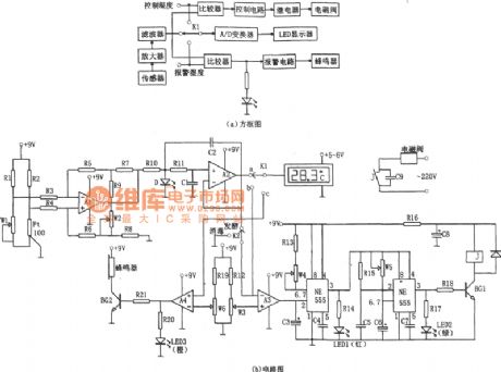
The alarming circuit is composed of comparator A4 and buzz circuit. When the temperature is more than 29 ℃, the A4 inverse end set potential compare with the A2 output. A4 outputs high level. The BG2 is conducted. It sounds bees alarm and at the same time the LED3 bright alarm lights (orange light) to remind the officer on duty to note out fault. It makes temperature control in the most suitable range. This circuit can make the temperature in 28 + 1 ℃, when the temperature is more than 29 ℃, the circuit will sound and light alarm signal to remind people. (View)
View full Circuit Diagram | Comments | Reading(721)
The gain -10 and +11 precision amplifier circuit diagram
Published:2011/6/28 4:26:00 Author:Rebekka | Keyword: precision amplifier
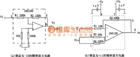
Gain + 11 precision amplifier circuit is shown in figure (b). The amplifier circuit has input impedance high magnification and the voltage is high. The voltage magnification is decided by: Av = type (1 + R2 / R1) = (1 + 100/10) = 1, the maximum gain error of the above two circuits is about 0.01%, The biggest nonlinear error is about 0.001%, the gain drift is about 2 x 10⁻⁶ / ℃. (View)
View full Circuit Diagram | Comments | Reading(608)
The liquid flowmeter
Published:2011/7/21 20:53:00 Author:qqtang | Keyword: liquid flowmeter
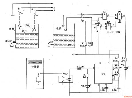
In industrial manufacturing, some situations need to measure the liquid flow and the rate. Here is to introduce the flowmeter which accumulates the liquid flowing time with ordinary octal bit computer, and then tests the distance between the poles according to the coverage of the liquid tank and the liquid level (set as 10cm), by which it computes the flow rate and volume of the liquid.The working principleThe liquid flowmeter consists of the liquid level detection control circuit, pulse generator and display circuit, see as figure 8-156.
(View)
View full Circuit Diagram | Comments | Reading(570)
Variable gain amplifier circuit diagram
Published:2011/6/30 2:51:00 Author:Rebekka | Keyword: Variable gain amplifier
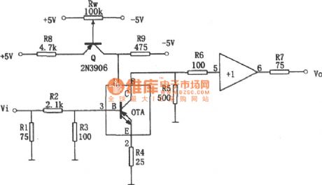

Figure 1 shows the variable gain amplifier (OPA660) circuit chart 1
The OPA660 OTA transconductance gm and static current Io the approximate relationship table.
The figure shows the circuit using transconductance op-amp integrated amplifier amplification OPA660 chip as components. The OPA660 integrated chips internal circuit has two components: The transconductance amplification and caching OTA part. About the internal structure of the integrated chips OPA660, the feet and the main parameters of the relevant material. The figure below is the table of the OPA660 OTA transconductance of gm and static current Io approximate relationship.
(View)
View full Circuit Diagram | Comments | Reading(858)
The high voltage output amplifying circuit composed of high op amp 3583
Published:2011/6/28 4:36:00 Author:Rebekka | Keyword: high voltage output, amplifying circuit
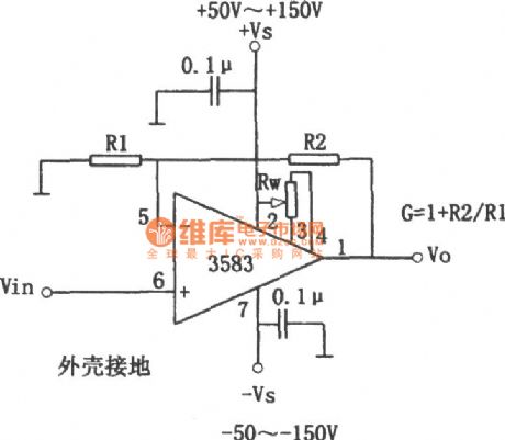
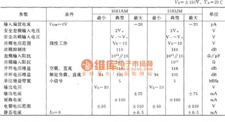
The figure shows the high voltage output amplifier circuit. The high operational amplifier 3583 chip supply voltage range is + 50 ~ + 150 V, the output voltage Vo range is + 40 ~ + 140 V. The voltage magnification is Av = 1 + R2 / R1. The maximum output current is + 75 mA. In 3583 integrated chips internal design overheated shut off the protection circuit, when the output of short circuit can protect integrated chips. It will not be damaged. The positive and negative power are decoupling capacitor. Its value is about 0.1 u F.
(View)
View full Circuit Diagram | Comments | Reading(1245)
10 A power amplifier circuit composed of the OPA541
Published:2011/7/2 1:30:00 Author:Rebekka | Keyword: power amplifier
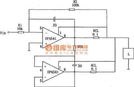
In actual work, in order to drive the motor or incentive the synchronous motor, it often need large current power amplifier circuit. A continuous outputing 10 A current power amplifier is shown in figure. The circuit uses two pieces of high power single piece operational amplifier OPA541 parallel work. The OPA541 monolithic op-amp can output 5 A current (its output current peak can reach up to 10 A), the two pieces of OPA541 parallel available sequential output 10 A current. (View)
View full Circuit Diagram | Comments | Reading(2379)
The car electric igniter (5)
Published:2011/7/21 20:42:00 Author:qqtang | Keyword: electric igniter
Here is to introduce the car electric igniter, which is made on the base of the 555 time-based integrated circuit, and it characterizes high igniting voltage(which can reach 15-20KV), low starting temperature of the engine, energy-saving and so on. The working principle The car electric igniter consists of the filter circuit, pulse oscillator circuit and switch booster circuit, see as figure 7-136.
The filter circuit consists of the filter capacitor C1-C3 and isolating diode VD1. (View)
View full Circuit Diagram | Comments | Reading(1611)
The bridge driving circuit composed of the OPA502
Published:2011/7/2 1:26:00 Author:Rebekka | Keyword: bridge driving
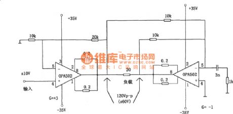
The figure shows the the bridge drive circuit composed of the OPA502. The OPA502 on the left uses the same phase input methods, so its input resistance is very high, the input signal is directly sent into the same phase input (pins 4), its positive and negative output terminals of the external SFCL RCL = 0.2 Ω. Thus the output current limit is 4 A. In the case of the parameters (the feedback resistance for 20 k Ω, inverse end resistance land is 10 k Ω), the voltage amplifier multiples is 3. The left output voltage of the OPA502 reaches to the load. (View)
View full Circuit Diagram | Comments | Reading(539)
The resistance electric bridge amplifying circuit composed of the INA102
Published:2011/6/28 4:42:00 Author:Rebekka | Keyword: resistance electric bridge , amplifying circuit
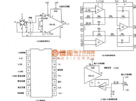
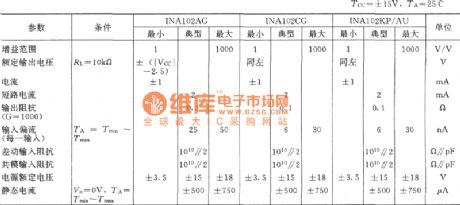
INA102 interior contains three integrated op-amp and resistance components. It has the ability of differential signal amplifier faint. It is often used as the data detection system preamplifier. When the voltage smaller (such as Av amplification times more than 10), the voltage and drift of disorders such as INA102 index can meet the requirements. When the voltage magnification is large (such as Av > 100 large). The bias current imbalance causing disorder voltage error will be bigger. It often uses graph (c) shows circuit to adjust the imbalance INA102 voltage.
(View)
View full Circuit Diagram | Comments | Reading(1104)
The biological electrical signals preamplifier circuit composed of the INA102
Published:2011/6/30 21:35:00 Author:Rebekka | Keyword: biological electrical signals , preamplifier
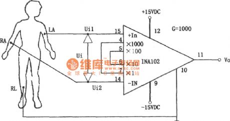
The figure shows the biological signals preamplifier circuit. They need to measure the biological electrical signals of the human body in the medical instrument, such as the electrocardiogram, eeg, etc. Due to the creatures signal is weak, the requirements of the amplifier circuit is very high. This circuit chooses the low power consumption meter with the integrated op-amp INA102. The features of the integrated chips INA102 are: Static current small (maximum is 750 mu A); The internal gain can pass the tube feet and change, the different connecting choice of gain is: l, 10, 100 and 1000 in the photo, pins 4 and 7 are connected with 5, and 6 pins and get the biggest gain 1000. (View)
View full Circuit Diagram | Comments | Reading(1223)
The ultrasonic back-up crashproof alarm (2)
Published:2011/7/22 22:45:00 Author:qqtang | Keyword: ultrasonic, crashproof alarm
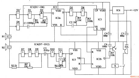
The working principle of the circuit The ultrasonic back-up crashproof alarm consists of the power supply circuit, ultrasonic emitting circuit, trigger circuit, low frequency oscillator, counter, ultrasonic reception process circuit and alarm circuit, see as figure 7-108.
The power supply circuit consist of the 3-terminal regulator integrated circuit IC6 and filter capacitors of C4 and C5.The ultrasonic emitting circuit consists of the emitter BI, the NOR gates D1-D4 inside the integrated circuit lC1(DI-D6), resistors of R1 and R2, resistor C1 and so on. (View)
View full Circuit Diagram | Comments | Reading(658)
The pulse delay circuit composed of gate circuit
Published:2011/6/29 2:58:00 Author:Rebekka | Keyword: pulse delay circuit , gate circuit
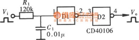
Pulse delay circuit will delay the output pulse that is relative to the input pulse for some time, but it will not change the width of the pulse. The main work principle of the circuit is to use the time delay function of the circuit. It delays the input pulse for a RC time. The figure shows the pulse delay circuit composed of gate circuit. (View)
View full Circuit Diagram | Comments | Reading(978)
| Pages:1452/2234 At 2014411442144314441445144614471448144914501451145214531454145514561457145814591460Under 20 |
Circuit Categories
power supply circuit
Amplifier Circuit
Basic Circuit
LED and Light Circuit
Sensor Circuit
Signal Processing
Electrical Equipment Circuit
Control Circuit
Remote Control Circuit
A/D-D/A Converter Circuit
Audio Circuit
Measuring and Test Circuit
Communication Circuit
Computer-Related Circuit
555 Circuit
Automotive Circuit
Repairing Circuit