
Circuit Diagram
Index 1448
LOOP_ANTENNA_PREAMPLIFIER
Published:2009/6/15 21:16:00 Author:May

This preamplifier has a built-in regeneration control boost gain selectivity. C1 is a single or multigang AM broadcast-band tuning capacitor. L1 is a ferrite loop antenna, tapped at about 15 to 25% of total turns. This circuit should prove useful for low-frequency (up to 3 MHz) reception, where a loop would be advantageous to reduce man-made noise pickup. (View)
View full Circuit Diagram | Comments | Reading(4474)
10_TO_1_Hz_TIMEBASE
Published:2009/6/15 21:16:00 Author:May
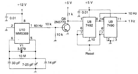
This system uses an MM5369 IC to derive a 60-Hz signal from a TV burst crystal (3579 MHz). V8 and V9 produce a 10-Hz and 1-Hz signal from this 60-Hz signal. Y1 can be any parallel-mode 3.579-MHz crystal. (View)
View full Circuit Diagram | Comments | Reading(1632)
LOW_POWER_ANTENNA_TUNER
Published:2009/6/15 21:15:00 Author:May
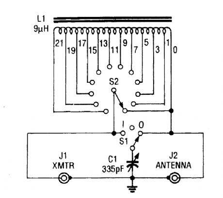
This antenna tuner is suitable for use with low-power (less than 5 W) transmitters or SW re-ceivers. 52 selects inductance and 52 connects the 365-pF capacitor to either the transmitter or the side of the inductor. The tiny tuner is comprised of a tapped inductor (L1) and a variable capacitor (C1), which is connected to the induc-tor through a center-off SPDT switch (S1). That switch arrangement permits the capacitor to be connected to either the input or the output of the circuit. (View)
View full Circuit Diagram | Comments | Reading(1736)
CRYSTAL_ACTIVITY_TESTER
Published:2009/6/15 21:15:00 Author:May
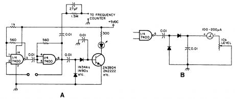
This circuit will check a crystal for activity.Two sections of a 7400 act as an oscillator and its out-put is rectified and drives an npn transistor that switches an LED (Fig.A).In Fig.B, a meter replaces the LED. (View)
View full Circuit Diagram | Comments | Reading(2)
MULTI_OUTPUT_TIMEBASE
Published:2009/6/15 21:12:00 Author:May
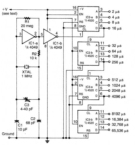
A 1-MHz oscillator drives a binary counter to produce pulse widths from 2 to 65,536 ms. V+ is any CMOS suitable level (5 to 15 V, etc.). (View)
View full Circuit Diagram | Comments | Reading(2101)
AUTOMATIC_TR_SWITCH
Published:2009/6/15 21:11:00 Author:May
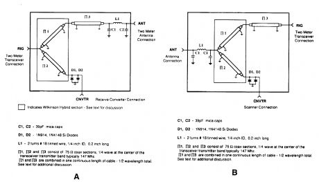
A pair of diodes and a quarter-wave transmission line are used as an automatic TR switch. D1 and D2 conduct during transmit periods, short-circuiting the scanner input. In th 1/4-wave line appears as an open circuit. In receive, the circuit acts as a Wilkinson power divider. (View)
View full Circuit Diagram | Comments | Reading(1045)
HEX_BUFFER_CRYSTAL_OSCILLATOR
Published:2009/6/15 21:09:00 Author:May
A 4049 single section acts as a crystal oscilla-tor, driving another section as a buffer, leaving four sections for other use. Use a 32- or 20-pF parallel resonant fundamental crystal. (View)
View full Circuit Diagram | Comments | Reading(796)
HF_BROADBAND_ANTENNA_PREAMP
Published:2009/6/15 21:06:00 Author:May

The HP/SW receiver preamplifier is comprised of a broadband toroidal transformer (L1-a and L1-b), LC network (corrtprised of a 1600-kHz, high-pass filter and a 32-MHz, low-pass filter), L2 and L3 (26 turns of #26 enameled wire wound on an Amidon Associates 7-50-2, red, toroidal core), a pair of resistive attenuators (ATTN1 and ATTN2), and a MAR-x device.Shown here is the composition of a basic 1-dB pi-network resistor antenuator. This is the method of supplying dc power to a preamplifier using only the RE coax cable. (View)
View full Circuit Diagram | Comments | Reading(2044)
EASY_CRYSTAL_IMPEDANCE_CHECKER
Published:2009/6/15 21:06:00 Author:May
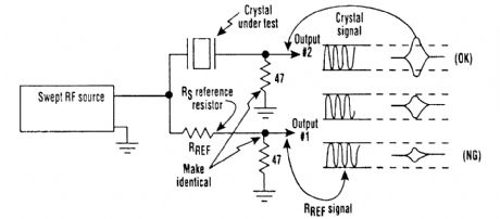
On occasion, micropro c es s ors/micro c omputers and microprocessor crystals just aren't compati-ble with each other. Many microprocessor data sheets specify maximum values for a crystal's equiv-alent series resistance (RS) that aren't met by some crystals advertised for microprocessor/ microcomputer use. As a result, a crystal with an RSvalue greater than the maximum specified for the chip might cause problems, such as a balky or even inoperative clock oscillator.To tackle this problem, a suspected crystal can be given a quick check forRS with a simple test setup that consists of a sweep generator, oscilloscope, and three resistors (see the figure). When the frequency source is brought to the crystal's frequency, output 2 will maximize. If it exceeds the am-plitude of output 1, the crystal's RS value will be less than the RS reference resistor's value. If it doesn't exceed output 1's amplitude, the crystal's RS value is too large. (View)
View full Circuit Diagram | Comments | Reading(873)
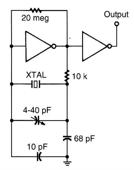
CRYSTAL_OSCILLATOR
Published:2009/6/15 21:04:00 Author:May
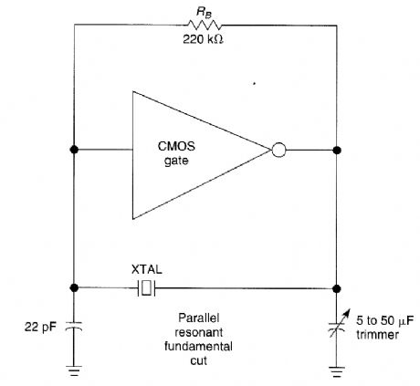
The CMOS amplifier is biased into the linear region by resistor RB. The pi-type crystal network (C1 and C2, and XTAL) provides the 180' phase shift at the resonant frequency which causes the circuit to oscillate. (View)
View full Circuit Diagram | Comments | Reading(1)
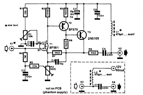
WIDEBAND_ANTENNA_PREAMPLIFIER
Published:2009/6/15 21:02:00 Author:May
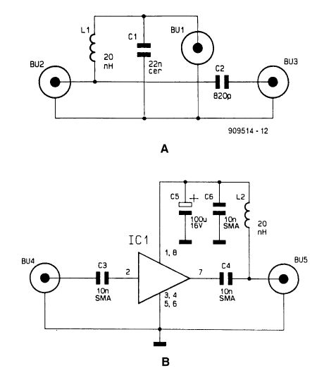
This wideband antenna preamplifier has a gain of around 20 dB from 40 to 860 MHz, covering the entire VHF, FM, commercial, and UHF bands. A phantom power supply provides dc to the preamp via the coaxial cable feeding the unit. (View)
View full Circuit Diagram | Comments | Reading(2512)
SIMPLE_BALUN
Published:2009/6/15 21:01:00 Author:May
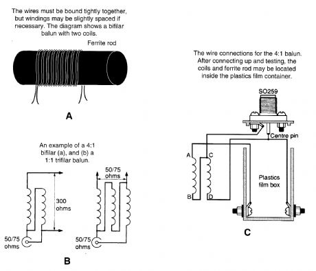
An old fettite rod from a junked broadcast receiver can be used to construct an antenna balun, as shown. (View)
View full Circuit Diagram | Comments | Reading(804)
VLF_60_kHz_ANTENNA_PREAMP
Published:2009/6/15 20:57:00 Author:May
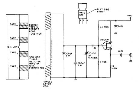
Suitable for 60-kHz standard frequency reception, here is a schematic for a FET preamp and antenna. (View)
View full Circuit Diagram | Comments | Reading(2737)
VLF_VHF_WIDEBAND_LOW_NOISE_ACTIVE_ANTENNA
Published:2009/6/15 20:55:00 Author:May
A 30- to 50-cm whip antenna provides reception from 10 kHz to over 220 MHz. T1, a dual-gate MOSFET, provides low noise, high-input impedance, and high gain.The circuit is powered via the coaxial cable used to connect the antenna to a receiver. (View)
View full Circuit Diagram | Comments | Reading(2442)
LOW_FREQUENCY_CRYSTAL_OSCILLATOR
Published:2009/6/15 20:55:00 Author:May
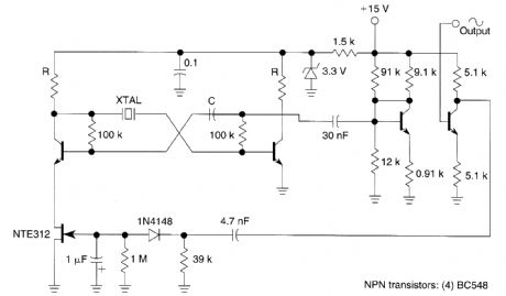
Q1, Q2, and the associated circuitry form a modified astable multivibrator in which the loop gain is automatically adjusted to the threshold of oscillation by means of field effect transistor Q3. Q4 lin-early amplifies the signal present at the collector of Q2 and isolates the oscillator section of the cir-cuit from the output. This stage features wideband operation and delivers a clean 2.5-V amplitude sine wave into a resistive load greater than or equal to 20 kΩ. The stage comprising Q5 has a voltage gain of 1 and its sole purpose is to isolate the nonlinear effects of rectifier Dl from the output. (View)
View full Circuit Diagram | Comments | Reading(2032)
10_MHz_FREQUENCY_COUNTER
Published:2009/6/15 20:51:00 Author:May
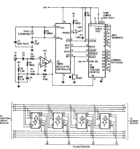
The circuit consists of an ICM7208 seven-decade counter (U1), an ICM7207A oscillator controller (U2), and a CA3130 biFET op amp (U3). Integrated circuit UI counts input signals, decodes them to 7-segment format, and outputs signals that are used to drive a 7-digit display. Integrated cir-cuit U2 provides the timing for UI, while U3 conditions the input signal to provide a suitable wave-form for input to UI. The 5.24288-MHz crystal frequency is divided by U2 to produce a 1280-Hz multiplexing signal at pin 12 of U2. That signal is input to UI at pin 16 and is used to scan the display digits in sequence. The cathodes of each digit are taken to ground several times each second, acti-vating any segments of the digits whose anodes are high as the result of decoding by UI. The crystal frequency is further divided to produce a short store pulse at pin 2 of U2, followed (after about 0.4 ms) by a short reset pulse at pin 14 of U2. The frequency of the pulses is determined by the state of U2 pin 11.When pin 11 of U2 is taken to ground through S1, the pulses occur every 2 seconds and cause U2 pin to go high for one second, which prevents additional input signals from entering UI. That causes the count latched in UI's internal counters to be transferred to the display.Integrated circuit U2 pin 13 then goes low for one second, allowing a new count to be entered into the seven decade counters of UI. That cycle is repeated, continuously updating the display every two seconds.When U2 pin 11 is taken to the positive supply rail (+5 V), the store and reset pulses occur at 0.2-s intervals, resulting in a 0.1-s count-period. Ten input pulses must be counted in order for a 1 to appear on the first digit, Dl, so that the frequency being measured is obviously 10 times larger than the frequency that is shown on the display. In that mode, the decimal points are driven by M and visually indicate that the 0.1-s count period is being used.The display must have at least seven 7-segment common-cathode multiplexed LED digits. Any common-cathode seven-segment display can be used; no particular display is specified. (View)
View full Circuit Diagram | Comments | Reading(3075)
DUAL_BAND_LOOP_ANTENNA_FOR_80__160_m
Published:2009/6/15 20:48:00 Author:May
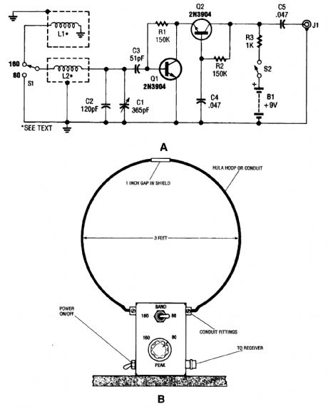
This antenna might help to reduce power-line noise. A plastic hula hoop or conduit 3 feet in diameter, covered with aluminum foil as a shield is used for L1 and L2. L1 is two turns and L2 is one turn, threaded through the loop. S1 selects 160- or 80-m operation. Q1 and Q2 form a preamplifier for the loop antenna. Do not transmit with this antenna-it is for receiving only. (View)
View full Circuit Diagram | Comments | Reading(2557)
2_MHz_FREQUENCY_COUNTER
Published:2009/6/15 20:48:00 Author:May
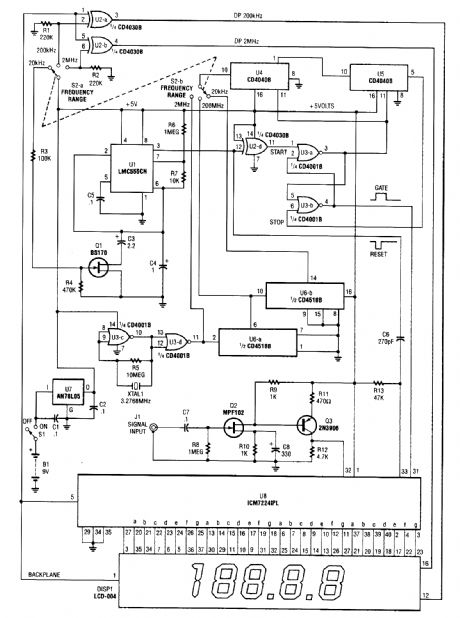

This is a schematic and block diagram of a 2-MHz frequency counter. It uses and LSI counter/display driver, LCD readout, and a,few logic chips for timebase and timing pulse circuitry. Q2 and Q3 form a signal (input) amplifier.The circuit contains a crystal oscillator built around U3-c and XTALl, which provides the pri-mary timing-reference signal. That signal is then divided twice to provide two additional timing ref-erences, giving the circuitry three selectable timing references. The ICM7224IPL is an integrated circuit that consists of the counter and display driver to drive the LCD-004 display. (View)
View full Circuit Diagram | Comments | Reading(3591)
8_CHANNEL_A_D_CONVERTER_FOR_PC_CLONESCont
Published:2009/6/15 4:18:00 Author:May
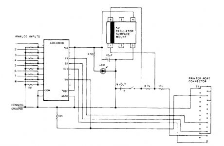
An A/D converter by National Semiconductor(ADC0838),converts 0- to 5-V analog inputs to adigital data format A 9-V battery is used.The converter connects to the pointer port connector viaa 25-pin connector (View)
View full Circuit Diagram | Comments | Reading(1648)
ADO_POLLER
Published:2009/6/15 4:15:00 Author:May
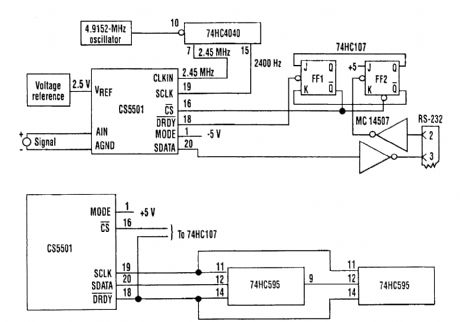
Because the CS5501 16-bit-delta-sigma analog-to-digital converter lacks a start convert com-mand, it converts continuously, outputting conversion words to its output register every 1024 cycles of its master clock. However, by incorporating a standard dual J-K flip-flop into the circuit, the ADC can be configured to output a single-conversion word only when it is polled.The CS5501 converter can be operated in its asynchronous communication mode (UART) to transmit one 16-bit conversion word when it is polled over an RS-232 serial line (see figure). A null character (all zeros) is transmitted to the circuit and sets the flip-flop FE2. The CS5501 can then out-put a single-conversion word, which is transmitted over the RS-232 line as two bytes with start and stop bits.The baud rate can be chosen by selecting the appropriate clock divider rate on the 74HC4040 counter/divider as the serial port clock (SLCK) for the ADC. This type of polled-mode operation is also useful when the ADC's output register is configured to operate in the synchronous-serial clock (SSC) mode. In this case, the converter will load one output word into a 16-bit serial-to-parallel reg-ister (two 74HC595 8-bit registers) when polled to do so (see figure). (View)
View full Circuit Diagram | Comments | Reading(1353)
| Pages:1448/2234 At 2014411442144314441445144614471448144914501451145214531454145514561457145814591460Under 20 |
Circuit Categories
power supply circuit
Amplifier Circuit
Basic Circuit
LED and Light Circuit
Sensor Circuit
Signal Processing
Electrical Equipment Circuit
Control Circuit
Remote Control Circuit
A/D-D/A Converter Circuit
Audio Circuit
Measuring and Test Circuit
Communication Circuit
Computer-Related Circuit
555 Circuit
Automotive Circuit
Repairing Circuit