
Circuit Diagram
Index 1447
POWER_ON_DELAY_CIRCUIT
Published:2009/6/15 22:06:00 Author:May
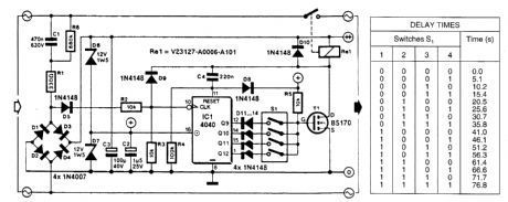
Using an IC to count ac mains pulses, the circuit produces 16 various delay times,where ac power is applied to a load after a preset interval. (View)
View full Circuit Diagram | Comments | Reading(2262)
LM38O_PERSONAL_STEREO_AMPLIFIER
Published:2009/6/15 22:05:00 Author:May
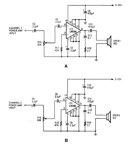
With the simple circuit, you can use your personal stereo to drive standard 8-Ω speakers. (View)
View full Circuit Diagram | Comments | Reading(817)
10_W_INVERTING_COMPOSITE_AMPLIFIER
Published:2009/6/15 22:04:00 Author:May
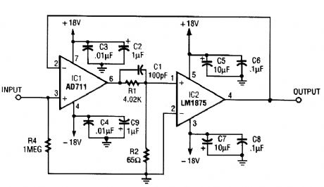
Using an LM1875,a 10-W amplifier can bebuild using just two IC devices The gam=R4/R3. Note that IC12 must be heatsinked (View)
View full Circuit Diagram | Comments | Reading(1438)
10_W_NONINVERTING_COMPOSITE_AMPLIFIER
Published:2009/6/15 22:03:00 Author:May
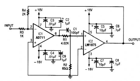
By using an LM1875, suitably heatsinked, a 10-W amplifier that uses two IC devices can be built, IC2 must be heatsinked. (View)
View full Circuit Diagram | Comments | Reading(1500)
MOSFET_POWER_AMPLIFIER
Published:2009/6/15 22:02:00 Author:May
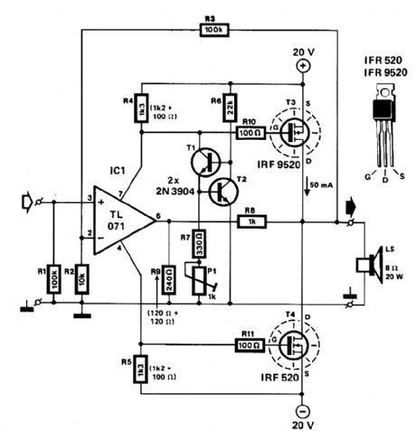
Two complementary MOSFETs are used to deliver 20 W into 8 Ω. A TL071 op amp is used as an input amplifier. The MOSFETs should be heatsinked with a heatsink of better than 5℃/W capability. THD is less than 0.15% from 100 Hz to 10 kHz. (View)
View full Circuit Diagram | Comments | Reading(3522)
INRUSH_CURRENT_LIMITER
Published:2009/6/15 22:02:00 Author:May
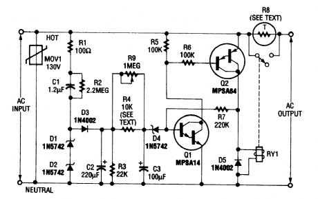
Q1 is an npn Darlington and Q2 is a pnp Darlington. MOV1 is a metal-oxide varistor and R8 is an NTC thermistor for limiting inrush current.This circuit limits ac line current to a load. When a predetermined interval has passed, RY1 shorts out thermistor or resistance RB. R4 can be 150 kΩ if R9 is not used. If power is removed, the circuit is ready for immediate restart. (View)
View full Circuit Diagram | Comments | Reading(4033)
A_33_W_BRIDGE_COMPOSITE_AMPLIFIER
Published:2009/6/15 21:56:00 Author:May
Two LM1875 ICs provide 33 W of audio. IC4 is used as a phase inverter. IC6 and IC2 must be heatsinked. (View)
View full Circuit Diagram | Comments | Reading(1032)
OFFSET_ADJUSTING_CURRENT_SOURCE
Published:2009/6/15 21:53:00 Author:May
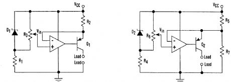
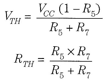


1. Though this setup can act as a cost-effective current source with an output accurate to 1%, the voltage offset will turn on the current source even when VCC equals Vin.2. Modifying the configuration of Figure 1 can rectify the problem of the current source being turned on by the voltage offset. The addition of R7 allows an adjustment that guarantees turn-off for any op-amp offset specification.
By carefully choosing components,you can create a cost effective circuit for a current Sourcewith an output that's accurate to 1%(Fig A). IOUT (the current flowing from the collector of Q1) is VCC-VIN(the voltage at the wiper of R3)divided by the value of R2.In some instances,it's important to be able to turn off the current source (within the limits of ICEO for Q1). Unfortunately, in about half of these cases,the offset voltage (Vos) of the op amp willturn the current Source on even when VCC=VIN That's because the offset voltage(when the norunverting input needs to be at a higher potential than the inverting input to get an output of 0V from the op amp) is impressed across R2 This offset voltage forces Q1 to turn on enough to yield a collector current of Vos divided by R2. Figure B offers a fix for this predicament The addition of R7 presents the emitter of Q2 with a Thevenin equivalent voltage and resistance represented by∶
The difference between VCC and VTH is VCC (R5/R5+R7) If VCC(R5/R5+R7) is set equal to the maximum Vos spec for the Op amp in question,the circuit is then guaranteed to turn off. This circuit hasan output current of VTH-VIN divided by RTHThe compromlse of Fig B does present another error term In the circuit The term (VTH-VIN)will have to be 2×VOS to guarantee a current output for whole population ofthe op amp chosen Thiserror can be made arbitrarily small (but not zero) by mcreasmg the voltage of D2 and VCC while raising the value of D2 and VCC while also ratsmg the value ofthe equivalent resistance RTH.
(View)
View full Circuit Diagram | Comments | Reading(879)
DUAL_AUDIO_AMPLIFIER
Published:2009/6/15 21:53:00 Author:May
View full Circuit Diagram | Comments | Reading(896)
HALF_WATT_SINGLE_CHANNEL_AUDIO_AMPLIFIER
Published:2009/6/15 21:31:00 Author:May
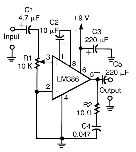
This circuit uses an LM386 IC and will work from 6- to 12-V battery sources. Output is about 0.5 W into 8 Ω. (View)
View full Circuit Diagram | Comments | Reading(859)
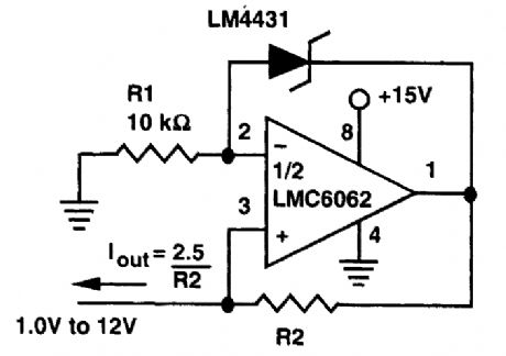
PRECISION_NEGATIVE_CURRENT_SOURCE
Published:2009/6/15 21:31:00 Author:May
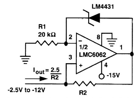
A National Semiconductor LM4431 reference and an LMC6062 op amp make up a negative cur-rent source. Current range is 1μA to 1mA. (View)
View full Circuit Diagram | Comments | Reading(895)
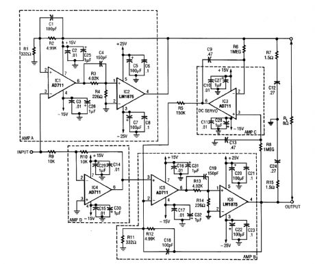
40_W_AMPLIFIER
Published:2009/6/15 21:30:00 Author:May
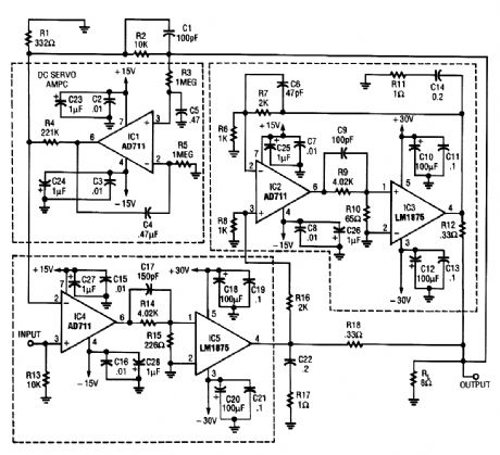
This circuit uses two LM1875 devices and a dc servo loop. This circuit provides 40-W output. IC3 and IC5 must be heatsinked. (View)
View full Circuit Diagram | Comments | Reading(1065)
BILATERAL_CURRENT_SOURCE
Published:2009/6/15 21:30:00 Author:May
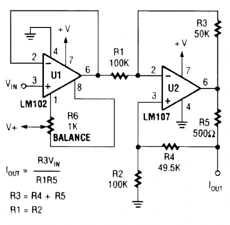
Using two op amps, this circuit produces current proportional to VIN (View)
View full Circuit Diagram | Comments | Reading(4)
PRECISION_POSITIVE_CURRENT_SOURCE
Published:2009/6/15 21:28:00 Author:May
An LM4431 precision 2.5-V reference and an LMC6062 op amp to make a positive current source, from 1mA to 10mA. (View)
View full Circuit Diagram | Comments | Reading(894)
CURRENT_SOURCE_FOR_LOW_RESISTANCE_MEASUREMENTS
Published:2009/6/15 21:27:00 Author:May
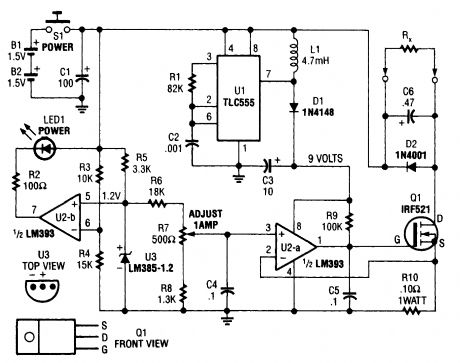


Useful for low-resistance measurements, this 1-A current source will produce 1 A in unknown resistance RX. For best results, RX should be less than 1 to 2Ω, because only 3V are available. U1 is a flyback converter to generate 9V for U2. (View)
View full Circuit Diagram | Comments | Reading(2003)
20_W___20_W_STEREO_AMPLIFIER
Published:2009/6/15 21:26:00 Author:May
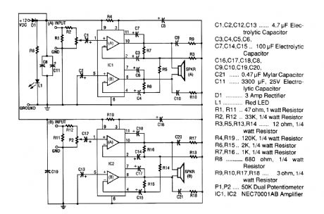
The 20-W + 20-W stereo amp consists of two complete, separate 20-W RMS bridge-type ampli-fiers. The input signal source is brought into the amplifier through the voltage divider network, which is made up of R1, R2, and P1. Resistor R1 provides a load impedance between the signal source and ground. Resistor R2 couples that signal to potentiometer P1.The signal is coupled by capacitor C1 to the noninverting (+) input (pin 1) of intemal amplifier (A) of IC1, where the signal is greatly amplified. Capacitor C2 couples the (+) input of the other (B) internal amplifier of IC1 to ground. That causes the input signal, which is referenced to ground, to be coupled to both amplifiers because both the inputs and outputs of IC 1 (A) and IC 1 (B) are connected in a bridge configuration. Notice that the output of IC1 (A) from pin 10 is connected to one side of the speaker and the output of IC1 (B) from pin 8 is connected to the other side of the speaker. That is why the speakers used cannot have one side connected to ground. Resistors R6 and R7 set the gain of the amplifier. Resistors R9 and R10 and capacitors C9 and C10 provide frequency stability ancl pre-vent oscillation. Capacitors C6 and C7 provide bootstrapping, which prevents distortion at low fre-quencies. LED L1 lights up by way of a series resistor connected from the anode to +12 Vdc when power is applied.Power for both IC1 and IC2 is brought in through D1 (to protect amplifiers from reverse polar-ity). Capacitor C11 provides additional power supply line filtering. This booster is capable of pro-ducing 20 W RMS output out of each channel. (View)
View full Circuit Diagram | Comments | Reading(771)
CRYSTAL_CONTROLLED_HARTLEY_OSCILLATOR
Published:2009/6/15 21:23:00 Author:May
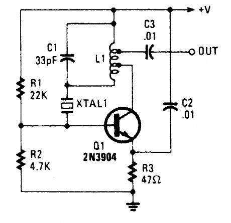
View full Circuit Diagram | Comments | Reading(777)
PIERCE_OSCILLATOR
Published:2009/6/15 21:22:00 Author:May
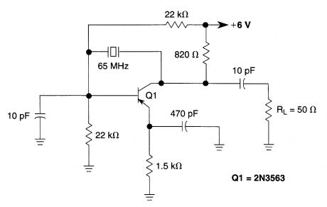
This Pierce oscillator uses a fundamental-mode 65-MHz crystal. (View)
View full Circuit Diagram | Comments | Reading(334)
WIDE_RANGE_CRΥSTAL_OSCILLATOR
Published:2009/6/15 21:21:00 Author:May
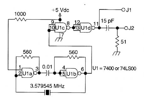
A circuit using one 7400 TTL IC can use crystals of the fundamental type, from 1 to about 13 MHz. Output is rich in harmonics, making this os-cillator useful for calibrations and test applica-tions. (View)
View full Circuit Diagram | Comments | Reading(654)
CRYSTAL_TESTER
Published:2009/6/15 21:19:00 Author:May
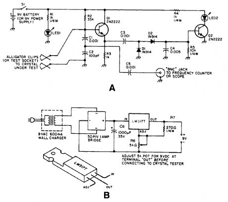
Q1 acts as a Colpitts crystal oscillator, and if the crystal under test is operational, the RF signal is rectified by D1 and D2, turning on Q2 and lighting indicator LED2. LED1 is a power indicator. (View)
View full Circuit Diagram | Comments | Reading(3928)
| Pages:1447/2234 At 2014411442144314441445144614471448144914501451145214531454145514561457145814591460Under 20 |
Circuit Categories
power supply circuit
Amplifier Circuit
Basic Circuit
LED and Light Circuit
Sensor Circuit
Signal Processing
Electrical Equipment Circuit
Control Circuit
Remote Control Circuit
A/D-D/A Converter Circuit
Audio Circuit
Measuring and Test Circuit
Communication Circuit
Computer-Related Circuit
555 Circuit
Automotive Circuit
Repairing Circuit