
Circuit Diagram
Index 1451
AUDIO_ALARM
Published:2009/6/14 21:59:00 Author:May
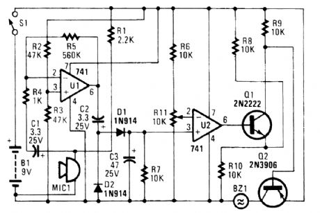
In the circuit, UI amplifies the audio picked up by the condenser microphone. Resistor RI limits current, while R2 and R3 center the output of the amplifier to 1/2 B+ to allow a singleended sup-ply to be used. Diodes Dl and D2 rectify the output of U1, and C3 filters the resulting pulsing dc.Thus, a dc voltage that is proportional to the ambient sound level is produced.That voltage is presented to the noninverting input of U2. The inverting input is provided with a reference voltage of between 0 and 1/2 B+, which is set by R11.As long as the noise level is low enough to keep the voltage at pin 3lower than the voltage at pin 2, the output of U2 stays low (approximately 1V). That is enough to bias Q1 partially on. A voltage divider, formed by R8/RIO and Q1 (when it's partially on), prevents Q2 from turning on.When the noise level is high enough to bring the voltage at pin 3 higher than the voltage at pin 2, the output of U2 goes high. That turns Q1 fully on and drives Q2 into saturation. The piezo buzzer then sounds until the power is cut off. (View)
View full Circuit Diagram | Comments | Reading(895)
CLOSED_LOOP_ALARM
Published:2009/6/14 21:40:00 Author:May
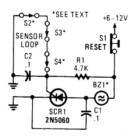
A string of three series-connected, normally closed switches are connected across the gate of an SCR. When one opens, the SCR triggers via R1, sounding an alarm. The alarm should be of the noninterrupting type. (View)
View full Circuit Diagram | Comments | Reading(1028)
WARBLE_ALARM
Published:2009/6/14 21:50:00 Author:May
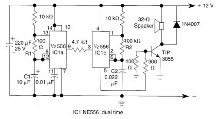
This circuit uses a 556 to first generate a low frequency square wave, that is modulated to pro-duce two alternate tones of about 400 and 500 Hz. Circuit generates warble alarm of European emer-gency vehicles. The frequencies of the oscillators are determined by the values of R1, C1 and R2, C2. (View)
View full Circuit Diagram | Comments | Reading(969)
STROBE_ALERT_SYSTEM
Published:2009/6/14 21:47:00 Author:May
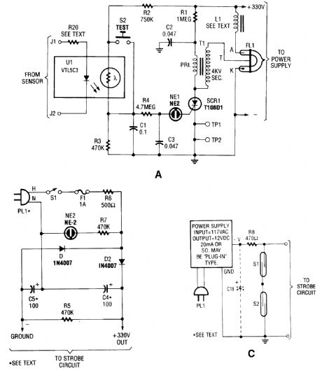
The circuit is activated by an LED/photoresistor isolator (U1), which is a combination of a light-dependent resistor (LDR) and an LED in a single package. That device was chosen because of its high isolation (2000 V) characteristic, which is necessary because the strobe part of the circuit is di-rectly connected to the ac line.The voltage divider is formed by R2, UI's internal resistance, and R3. When UI's internal LED is off, UI's internal LDR has a very high resistance-on the order of 10 MO. The voltage applied to NE1 is considerably below its ignition voltage of approximately 90 Vdc.The optoisolator's internal LED is activated by a dc signal supplying 20 mA. The external sen-sor(s) that supply the signal are connected to the strobe part of the circuit at J1 and J2.When the internal LED lights, the LDR's resistance decreases to around 5 kΩ. Under that con-dition, about 125 Vdc is applied across C1, R4, and C2. The neon lamp periodically fires and extin-guishes as capacitor C3 charges through R4, and discharges via NE1 and the SCR gate.Rests!or R4 restricts the current input to C3, and thereby controls the firing rate of NEl-about three times per second. The discharge through NE1 is applied to the gate of SCR1.SCR1, a sensitive-gate unit, snaps on immediately when NE1 conducts, which completes the ground circuit for transformer T1 (a 4-kV trigger transformer). As SCR1 toggles on and off in time with the firing of NE1, capacitor CZ (connected in parallel with T1's primary) charges via RI, and then discharges very rapidly through T1's primary winding. A voltage pulse is applied to the trigger input of ELI, a Xenon flash lamp.It is important to remember that the circuit is connected directly to the ac line. Resistor R6 is in-cluded to limit the amount of line current available to the circuit. The value of R6 can be decreased if you intend to modify the circuit for more flash power.Warning: Even though the circuit is fuse-protected, it can still be dangerous if handled care-lessly. (View)
View full Circuit Diagram | Comments | Reading(1834)
DELAYED_ALARM
Published:2009/6/14 21:42:00 Author:Celina
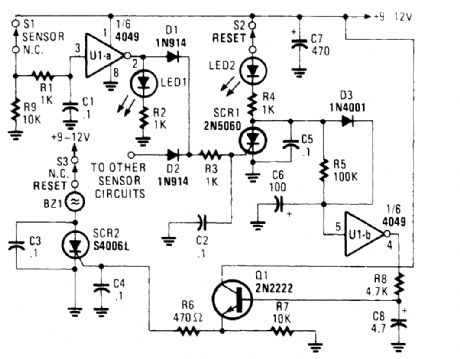
The alarm/sensor circuit shown is built around two SCRs, a transistor, a 4049 hex inverter, and a few support components, all of which combine to form a closed-loop detection circuit with a delay feature. The delay feature allows you to enter a protected area and deactivate the circuit before the sounder goes off.Assuming that the protected area has not been breached (i.e., S1 is in its normally-closed posi-tion), when power is first applied to the circuit, a positive voltage is applied to the input of UI-a through 51 and RI, causing its output to go low. That low is applied to the gate of SCR1, causing it to remain off. At the same time, C6 rapidly charges toward the +Tsupply rail through S2, LED2, R4, and D3. The charge on C6 pulls pin 5 of UI-b high, causing its output at pin 4 to be low. That low is ap-plied to the base of Q1, keeping it off. Because no trigger voltage is applied to the gate of SCR2 (via Q1), the SCR remains off and BZ1 does not sound.But should S1 open, the input of UI-a is pulled low via R9, forcing the output of UI-a high, light-tng LED1. That high is also applied to the gate of SCR1 through Dl and R3, causing SCR1 to turn on.With SCR1 conducting, the charge on CG decays, the input of UI-b at pin 5 is pulled low, forcing its output high, slowing charging C8 through R8 to a voltage slightly less than the positive supply rail.Transistor Q1 remains off until C8 has charged to a level sufficient to bias Q1 on, allowing suffi-cient time to enter the protected area and disable the alarm before it sounds. Once C8 has developed a sufficient charge, Ql turns on and supplies gate current to SCR2 through R6, causing the SCR to turn on and activate BZ1. If the circuit is reset before the delay has timed out, no alarm will sound.The delay time can be lengthened by increasing the value of either or both C6 and R5; decreas-tng the value of either or both of those components will shorten the delay time.All of the switches used in the circuit are of the normally-closed (NC) variety. Switch 51 can be any type of NC security switch. Switch 52 can be either a pushbutton or toggle switch. Because 53 is used to disable the sounder (BZl) only, anything from a key-operated security switch to a hidden toggle switch can be used. (View)
View full Circuit Diagram | Comments | Reading(1342)
DOOR_MINDER
Published:2009/6/14 21:45:00 Author:Celina
This circuit monitors a door to detmrmine if it has been left open.After 24 seconds, the alarm sounds.S1 is a magnetic sensor. The alarm is an electronic chime sound that is struck once per second. (View)
View full Circuit Diagram | Comments | Reading(1120)
LOW_DROP_OUT_REGULATOR
Published:2009/6/23 4:06:00 Author:jailer
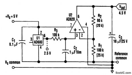
This low-dropout reference produces a 4.5-V output from a supply just a few hundred millivolts greater. With 1-mA dc Ioading, it maintains a stable 4.5-V output for inputs down to 4.7 V. (View)
View full Circuit Diagram | Comments | Reading(789)
LEAD_ACID_BATTERY_CHARGER
Published:2009/7/6 4:27:00 Author:jailer
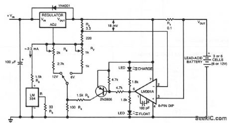
This circuit furnishes an initial voltage of 2.5 V per cell at 25℃ to rapidly charge a battery. The charging current decreases as the battery charges, and when the current drops to 180 mA, the charging circuit reduces the output voltage to 2.35 V per cell, leaving the battery in a fully charged state. This lower voltage prevents the battery from overcharging, which would shorten its life.
The LM301A compares the voltage drop across R1 with an 18 mV reference set by R2. The comparator's output controls the voltage regulator, forcing it to produce the lower float voltage when the battery-charging current, passing through R1, drops below 180 mA. The 150 mV difference between the charge and float voltages is set by the ratio of R3 to R4. The LEDs show the state of the circuit.
Temperature compensation helps prevent overcharging, particularly when a battery undergoes wide temperature changes while being charged. The LM334 temperature sensor should be placed near or on the battery to decrease the charging voltage by 4 mV/℃ for each cell. Because batteries need more temperature compensation at lower temperatures, change R5 to 30 Ωfor a tc of -5 mV/℃ per cell if application will see temperatures below -20℃.
The charger's input voltage must be filtered dc that is at least 3 V higher than the maximum required output voltage: approximately 2.5 V per cell. Choose a regulator for the maximum current needed: LM371 for 2 A, LM350 for 4 A, or LM338 for 8 A. At 25℃ and with no output load, adjust R7 for a VOUT of 7.05 V, and adjust R8 for a VOUT of 14.1V. (View)
View full Circuit Diagram | Comments | Reading(3792)
NUCLEAR_REACTOR_STARTUP_CONTROL
Published:2009/7/13 1:05:00 Author:jailer


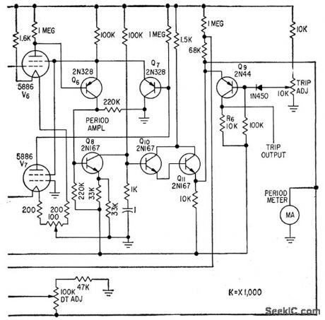
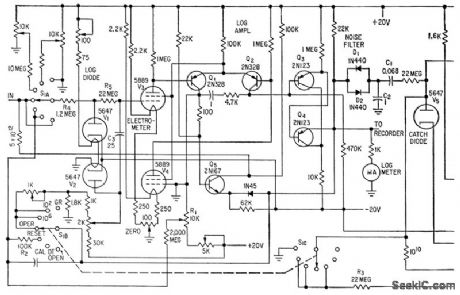

Logarithmic and period amplifers provide required wide indicating range without switching. Use of log diode V1 in series bock to back with V2 provides nonlinear element in which effects of changes in cathode temper ature and supply voltage are balanced out.V1 drives log amplifier consisting of balanced electrometer tubes V3 and V4, differential stage Q1-Q2, and cascaded emitter-followers Q3 and Q4. Period ampliler is a feedback-type differentiating circuit.-E. J. Wade and D.S. Davidson, Transistor Amplifers for Reactor Controls, Electronics, 32:21,p52-53. (View)
View full Circuit Diagram | Comments | Reading(951)
PARALLEL_LOOP_ALARM
Published:2009/6/14 21:39:00 Author:jailer
Four paraJlel switches are used to monitor four positions. When a closure occurs on any switch, SCR1 triggers, which sounds the alarm.The alarm should be of the noninterrupting type. (View)
View full Circuit Diagram | Comments | Reading(740)
SERIES_PARALLEL_LOOP_ALARM
Published:2009/6/14 21:38:00 Author:jailer
Two SCRs are used with two sensor loops. One loop uses series switches, the other loop parallel switches. When a switch actuation occurs, the SCR triggers. The alarm should be a noninterrupting type. (View)
View full Circuit Diagram | Comments | Reading(899)
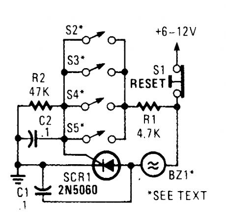
MULTI_LOOP_PARALLEL_ALARM
Published:2009/6/14 21:35:00 Author:jailer
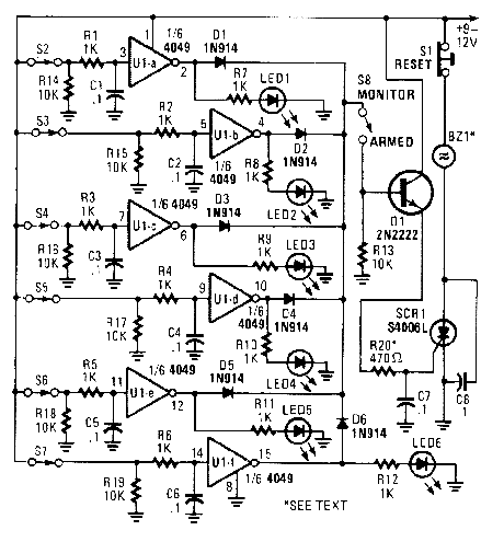
This alarm has status LEDs connected across each inverter output to indicate the status of its as-sociated sensor. S8 is used to monitor the switches via the LEDs, or to trigger an alarm via Q1 and SCR1. BZ1 should be a suitable alarm of the noninterrupting type. (View)
View full Circuit Diagram | Comments | Reading(806)
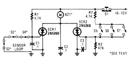
HIGH_POWER_ALARM_DRIVER
Published:2009/6/14 21:32:00 Author:jailer
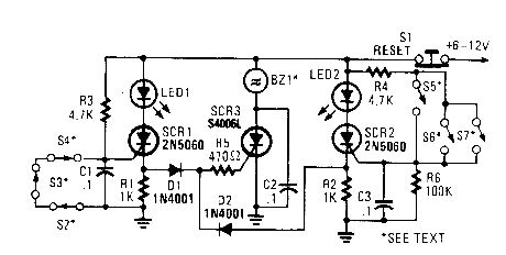
In this circuit, a low-powered SCR is used to trigger a higher powered SCR. When a switch is opening (52, 53, 54) or closing (55, 56, 57), ei-ther SCR1 or SCR2 triggers. This triggers SCR3 via Dl, D2, and R5. BZ1 is a high-powered alarm of the noninterrupting type. (View)
View full Circuit Diagram | Comments | Reading(863)
Gas water heater combustion detector circuit diagram
Published:2011/7/20 20:07:00 Author:Ecco | Keyword: Gas , water heater, combustion , detector
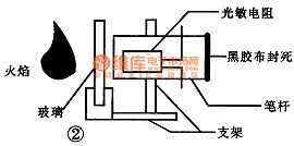
Domestic gas water heaters should be installed in well-ventilated place which is outside of the bathroom, but this, people in the bathroom can not clearly observe the combustion heater. Sometimes water heater can not ignite due to insufficient water pressure or other reasons, or being blown off after ignite, people can discover in time, only through the water temperature changes to determine the water heater. So the designer makes a simple and convenient water heater combustion detection device for people observing water heater combustion without going out.
(View)
View full Circuit Diagram | Comments | Reading(674)
Data gain high speed cascade amplifier circuit composed of the PGA102
Published:2011/6/30 10:31:00 Author:Rebekka | Keyword: Data gain high speed , cascade amplifier
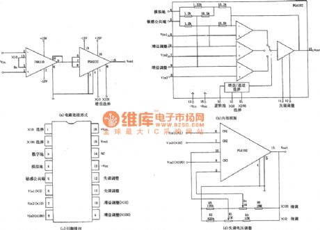
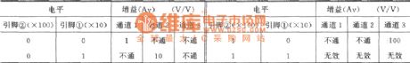
The the relationship of the gain value and control the level:
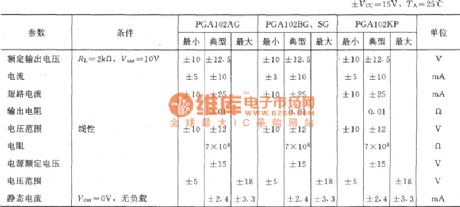
The main parameters of the integrated chip's PGA102:
The figure shows the data gain high speed cascade amplifying circuit. This circuit is composed of the umerical control instrument amplifier INA110 and the gain programmable integrated op-amp PGA102. When the 3 pin of the INAll0 connects with the pins 13, the voltage amplifier multiples is Av = 10. The control of the gain circuit is compeleted by the first level 2 PGA102 integrated op-amp.
(View)
View full Circuit Diagram | Comments | Reading(588)
The gain automatic controllable shift amplifier circuit composed of PGA202
Published:2011/6/30 10:20:00 Author:Rebekka | Keyword: gain automatic, controllable shift amplifier
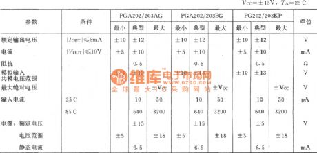
The figure shows the automatic gain control shift amplifier circuit. This circuit consists of four parts: The amplification unit circuit gain programmable instrument (with amplification integrated chips PGA202 component). It adds and subtracts counter unit, two-way comparator unit and 10 V benchmark voltage source. The internal structure of PGA202 is shown in figure (b), its gain can be controlled by TTL level, the integrated chips and single-chip microcomputer are easily interfaced. The PGA202 for mosfet input type and includes the conductive road, it can realize across the bandwidth in different gain almost the same. (View)
View full Circuit Diagram | Comments | Reading(557)
High input impedance three op amp differential amplifier circuit diagram
Published:2011/6/27 4:59:00 Author:Rebekka | Keyword: High input impedance, three op amp differential amplifier
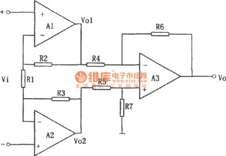
The circuit is mainly used for the monitor the signal pre-amplification or amplification of various data, which is sometimes referred to be used as data amplifier circuit. Figure shows a four-op-amp OP-09A integrated chip. In order to increase input impedance. It still uses the same phase of adding signal voltage input method. In order to ensure the two sources are added to the op amp's inverting input. It uses the two-phase amplifier A1 and A2 to form the first stage amplifier. Table 1 shows the OP-09A quad op amp integrated amplifier electrical characteristics table. (View)
View full Circuit Diagram | Comments | Reading(942)
Hatch temperature controller circuit diagram
Published:2011/6/28 2:13:00 Author:Rebekka | Keyword: Hatch temperature controller
The figure shows the hatch temperature control circuit. This circuit is composed of the temperature detection circuit, temperature control circuit and power outages alarm circuit etc. The temperature measurement circuit is an unbalanced bridge, and it uses gauge head A for instructions. The electric bridge is a negative temperature coefficient and has high sensitivity MF51 thermal resistor. Along with the hatch of the temperature in the cabinet constant temperature is different, the resistance of the MF51 changes. The potential of corresponding bridge two points A and B changes. It passes the 50 ttA magnetoelectric meter pointer to reflect the change of the temperature changes. (View)
View full Circuit Diagram | Comments | Reading(689)
Variable threshold over-current and over voltage protection circuit diagram
Published:2011/5/12 21:47:00 Author:Rebekka | Keyword: Over-current protection, over voltage protection
The circuit will set the corresponding reference threshold for effective protection of the load depending on the actual voltage and current of the load. The whole circuit is composed of over current, over voltage detection, signal amplifier and control signal output circuit, manual start, stop control circuit and thyristor trigger circuit. (View)
View full Circuit Diagram | Comments | Reading(1547)
Monolithic over and under voltage protection circuit diagram
Published:2011/5/12 21:34:00 Author:Rebekka | Keyword: Monolithic over and under voltage protection
The over and under voltage protection circuit is composed of the six Schmitt trigger CD4584 . When it is over-voltage or under voltage. The circuit will sound siren and cut off the working power supply of the controlled circuit by relay. (View)
View full Circuit Diagram | Comments | Reading(2865)
| Pages:1451/2234 At 2014411442144314441445144614471448144914501451145214531454145514561457145814591460Under 20 |
Circuit Categories
power supply circuit
Amplifier Circuit
Basic Circuit
LED and Light Circuit
Sensor Circuit
Signal Processing
Electrical Equipment Circuit
Control Circuit
Remote Control Circuit
A/D-D/A Converter Circuit
Audio Circuit
Measuring and Test Circuit
Communication Circuit
Computer-Related Circuit
555 Circuit
Automotive Circuit
Repairing Circuit