
Circuit Diagram
Index 307
Spy phone transmitter
Published:2012/10/11 2:30:00 Author:muriel | Keyword: Spy phone, transmitter
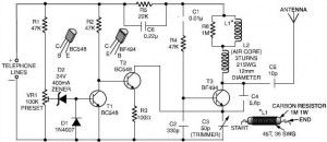
Here is a very simple telephone broadcaster or transmitter which can be used to eavesdrop on a telephone conversation. The circuit can also be used as a wireless telephone amplifier.One important feature of this phone transmitter is that the circuit derives its power directly from the active telephone lines, and thus avoids use of any external battery or other power supplies.This not only saves a lot of space but also money. It consumes very low current from telephone lines without disturbing its performance. The phone bug transmitter is very tiny and can be built using a single -IC type veroboard that can be easily fitted inside a telephone connectin box of 3.75cm x 5cm.
The spy phone transmitter consists of two sections, namely, automatic switching section and FM transmitter section.
Spy phone transmitter circuit diagram
Automatic switching section comprises resistors R1 to R3, preset VR1, transistor T1 and T2, zener D2 and diode D1. Resistor R1, along with preset VR1, works as a voltage divider. When voltage across the telephone lines is 48V DC, the voltage available at wiper of preset VR1 ranges from 0 to 32V (adjustable).
The switching voltage of the circuit depends on zener breakdown voltage and switching voltage of the transistor T1. Thus, if we adjust preset VR1 to get over 24.7 volts, it will cause the zener to breakdown and transistor T1 to conduc. As a result collector of transistor T1 will get pulled towards negative supply, to cut off transistor T2. At this stage, if you lift the handset of the telephone, the line voltage drops to about 11V and transistor T1 is cut off. As a result, T2 gets forward biased through R2 to provide a DC path for T3 used in the following FM transmitter section.
The low-power FM transmitter section comprises oscillator transistor T3, coil L1 and a few other components. T3 works as a common-emitter RF oscillator, with T2 serving as an electronic “on/off” switch. The audio signal available across the telephone lines automatically modulates oscillator frequency via T2 along with its biasing R3. The modulated RF signal is fed to the antenna. The telephne conversation can be heard on an FM receiver remotely when it is tuned to the transmitter frequency.
(View)
View full Circuit Diagram | Comments | Reading(1392)
Simple code lock circuit
Published:2012/10/11 2:30:00 Author:muriel | Keyword: Simple code, lock
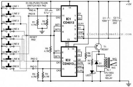
This simple code lock circuit described here is of an electronic combination lock for daily use. It responds only to the roght sequence of four digits that are keyed in remotely. If a wrong key is touched, it resets the lock. The lock code can be set by connectiong the line wires to the pads A, B, C and D in the figure. For example, if the code is 1756, connect line 1 to A, line 7 to B, line 5 to C, line 6 to D and rest of the lines-2,3,4,8 and 9 to the reset pad as shown by dotted lines in the schematic.
Code lock circuit schematic
(View)
View full Circuit Diagram | Comments | Reading(1401)
Luggage, bike security alarm
Published:2012/10/11 2:29:00 Author:muriel | Keyword: Luggage, bike, security alarm

This luggage or bike alarm can be used while travelling by trains or bus and we generally lock our luggage using a chain-and-lock arrangement. But, still we are under tension, apprehending that somebody may cut the chain and steal our luggage. Here is a simple circuit to alarm you when somebody tries to cut the chain.
T1 enables supply to the sound generator chip when the base current wire (thin enameled copper wire of 30 to SWG, used for winding transformers) loop arround the chain is broken by somebody, the base of T1, which was earlier tied to positive rail, gets opened. As a result, T1 gets forward biased to extend the positive supply to the alarm circuit. In idle mode, the power consumption of the circuit is minimum and thus it can be used for hundred of travel hours.
Luggage chain alarm circuit diagram
(View)
View full Circuit Diagram | Comments | Reading(867)
Lightning detector circuit
Published:2012/10/11 2:29:00 Author:muriel | Keyword: Lightning detector
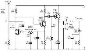
This DIY lightning detector circuit is a very sensitive static electricity detector that can provide an early warning of approaching storms from inter-cloud discharge well before an earth-to-sky return strike takes place. An aerial (antenna) formed of a short length of wire detects storms within a two mile radius.The circuit emits an audible warning tone from a piezo buzzer, or flashes an LED for each discharge detected, giving you advance warning of impendig storms so that precautions may be observed. The primary feature in the lighting detector is the circuit’s ability to be set close to self-oscillation, with its relaxation optimised via the bias resistor values shown in the circuit diagram. The oscillator is dc coupled and feedback is routed through the collector of TR1 to the base of TR2, while the overall loop gain is set with the multiturn(12, 18 or 22) preset VR1.
Lightning detector setting upTo set up the lightning sensor, adjust preset VR1 for oscillation by monitoring test point TP1, which should be at roughly 7volts peak-to-peak. Test point TP2 should be at +6V dc. Now readjust VR1 back slightly to stop oscillation; use a screwdriver to touch the aerial-side of C1 several times; the alarm should sound for 1 or 2 seconds then stop. If it continues, make a very small adjustment back and recheck. The other method is to electrostatically charge a plastic ruler and then draw your finger close to discharge, about two meter away from the aerial.
Lightning detector schematic
(View)
View full Circuit Diagram | Comments | Reading(2904)
Electronic dog repellent project
Published:2012/10/11 2:29:00 Author:muriel | Keyword: Electronic dog, repellent project
The electronic dog repellent circuit diagram below is a high output ultrasonic transmitter which is primarily intended to act as a dog and cat repeller, which can be used individuals to act as a deterrent against some animals. It should NOT be relied upon as a defence against aggressive dogs but it may help distract them or encourage them to go away and do not consider this as an electronic pest repeller.The ultrasonic dog repellant uses a standard 555 timer IC1 set up as an oscillator using a single RC network to give a 40 kHz square wave with equal mark/space ratio. This frequency is above the hearing threshold for humans but is known to be irritating frequency for dog and cats.
Since the maximum current that a 555 timer can supply is 200mA an amplifier stage was required so a high-power H-bridge network was devised, formed by 4 transistors TR1 to TR4. A second timer IC2 forms a buffer amplifier that feeds one input of the H-bridge driver, with an inverted waveform to that of IC1 output being fed to the opposite input of the H-bridge.For more electronic dog repeller circuits check the related links bellow.
Cat and dog repellent circuit diagram
(View)
View full Circuit Diagram | Comments | Reading(1470)
Remote audio level indicator
Published:2012/10/11 2:28:00 Author:muriel | Keyword: Remote, audio, level indicator
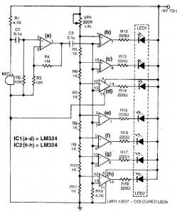
The normal level-indicator circuits which are available in the market require connections to be made to the output of the player, which may not be easily accessible. The audio level indicator circuit described here removes this restriction as it may be placed close to the player’s speakers and yet the desired effect can be realised. As shown in the circuit, signals are picked up by the condenser microphone, which get further amplified by the noninverting amplifier built around one of the four op-amps of LM324. The remaining three, along with four op-amps of the second LM324, are used as seven comparators to work as the level detector, giving seven output levels through seven coloured LEDs.
The sensitivity of the audio level indicator circuit may be improved by varying the 220k potentiometer. If a fine adjustment is desired, a 4.7-kilohm potentiometer may be connected in series resistors with the 220k potentiometer.
Remote audio level indicator circuit diagram
(View)
View full Circuit Diagram | Comments | Reading(1653)
Quality FM transmitter circuit
Published:2012/10/11 2:28:00 Author:muriel | Keyword: Quality, FM transmitter
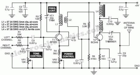
This house FM transmitter for your stereo or any other amplifier provides a good signal strength up to a distance of 500 meters with a power output of about 200 mW. It works off a 9V battery.
The audio-frequency modulation stage is built around transistor BF494 (T1), which is wired as a VHF oscillator and modulates the audio signal present at the base. Using preset VR1, you can adjust the audio signal level.Audio FM transmitter circuit diagram
The VHF frequency is decided by coil L1 and variable capacitor VC1. Reduce the value of VR2 to have a greater power output.The next stage is built around transistor BC548 (T2), which serves as a Class-A power amplifier. This stage is inductively coupled to the audio-frequency modulation stage. The antenna matching network consists of variable capacitor VC2 and capacitor C9. Adjust VC2 for the maximum transmission of power or signal strength at the receiver.
If you design a good pcb layout you can use it as a car fm transmitter.For frequency stability, use a regulated DC power supply and house the transmitter inside a metallic cabinet. For higher antenna gain, use a telescopic antenna in place of the simple wire. Coils L1 and L2 are to be wound over the same air core such that windings for coil L2 start from the end point for coil L1. Coil windingdetails are given below:L1: 5 turns of 24 SWG wire closely wound over a 5mm dia. air coreL2: 2 turns of 24 SWG wire closely wound over the 5mm dia. air coreL3: 7 turns of 24 SWG wire closely wound over a 4mm dia. air coreL4: 5 turns of 28 SWG wire on an intermediate-frequency transmitter (IFT) ferrite coreCheck the related posts for some stereo fm transmitter circuits.
(View)
View full Circuit Diagram | Comments | Reading(2267)
Simple metal detector circuit
Published:2012/10/11 2:28:00 Author:muriel | Keyword: Simple, metal detector
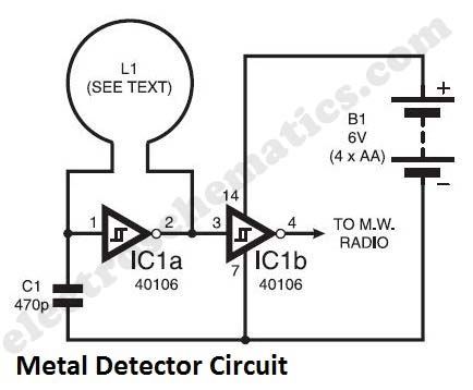
The metal detector circuit shown here must represent the limits of simplicity for a metal detector, yet the design works surprisingly well. It uses just one 40106 hex Schmitt inverter IC, a capacitor and a search coil – and of course the batteries. A lead from IC1b pin 4 needs to be attached to a medium wave radio aerial, or it should be wrapped around the radio. It can be used even like those hand held metal detectors. As shown, the metal detector gives a respectable range for beat frequency operation (bfo) up to 90mm for a bottle-top. In fact, for the ultimate in simplicity, capacitor C1 may be omitted. In this way the author achieved am amazing 150mm range for the bottle-top. However, with the frequency then being raised to more than 4MHz, instability becomes a significant problem.
As shown, the circuit oscillates at around 230kHz. One may also experiment with the frequency by changing the value of C1. A Faraday shield may be added to reduce ground effect and capacitive coupling, and this is wired to 0V.
Since the inductor resists rapid changes voltage, the charging of C1 is slightly delayed as the logic level at IC1a pin 2 changes. This sets up a rapid oscillation, which is picked up by a MW radio. Any changes in the inductance of the search coil (through the presence of metal) bring about a change to the oscillator frequency. Although 230kHz is out of range of the Medium Wave band, an MW radio will clearly pick up harmonics of this frequency.
Metal detector calibrationThe making of search coil L1 allows a lot of room for error and is far from critical. The author used seventy turns 30 s.w.g. (0,315mm) enamelled copper wire on a 120mm diameter former.The metal detector is set up by tuning the MW radio to pick up a whistle. Not every such harmonic works well, and the most suitable one needs to be found. The presence of metal will clearly change the tone of the whistle.
Metal detector faqThis is not an industrial or security metal detector and is not even close to loma or eriez metal detection products. It’s just a portable but not a hand held metal detector.
Metal Detector circuit diagram
(View)
View full Circuit Diagram | Comments | Reading(3231)
BLW96 amplifier
Published:2012/10/11 2:26:00 Author:muriel | Keyword: BLW96,amplifier
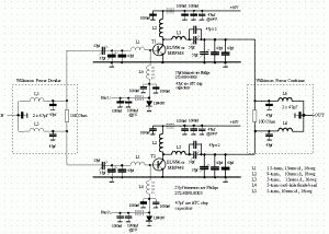
BLW96 is a HF/VHF power transistor intended for use in class-A, AB and B operated high power industrial and military transmitting equipment in the h.f. and v.h.f. band.
BLW96 amplifier 450W 50MHz
A possible downside of this is that they may not have less gain at 50MHz compared to a VHF transistor but, as can be seen in Figure 1, at least 12 to 14dB of gain can be obtained at 50MHzz (the BLW96 performs well at 70MHz as well incidentally).To achieve the required output in this design, two BLW96s have been paralleled to provide 450 watts with just a little over 20 watts of drive. The input power is split using a Wilkinson power divider whose design was extensively discussed in SIX NEWS #33, The output of the two amplifiers are combined using the same, only reversed, circuit. Under normal circumstances the 100 ohm resistor connecting the two output (or input) ports does not dissipate very much power, but during tune-up it is possible that it could.
As it is important that these resistors are truly non-inductive, the design uses rather special devices.These are ‘bolt-down’ 100 Ohm terminating resistors with two flying leads to connect to the circuit board – they look rather like transistors in construction. (View)
View full Circuit Diagram | Comments | Reading(1638)
Hearing aids circuit
Published:2012/10/11 2:26:00 Author:muriel
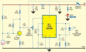
This low-cost, general-purpose electronic hearing aids works off 3V DC (2×1.5V battery). Transistor T1 and associated components form the audio signal preamplifier for the acoustic signals picked up by the condenser microphone and converted into corresponding electrical signals.The medium-power amplifier section is wired around popular audio amplifier IC TDA2822M (not TDA2822). This IC, specially designed for portable low-power applications, is readily available in 8-pin mini DIP package. Here the IC is wired in bridge configuration to drive the 32-ohm general-purpose monophonic earphone.
The audio output of this hearing aid circuit is 10 to 15 mW and the quiescent current drain is below 1 mA. The circuit can be easily assembled on a veroboard. For easy assembling and maintenance, use an 8-pin DIP IC socket for TDA2822M.
Hearing aids circuit wiring diagram
(View)
View full Circuit Diagram | Comments | Reading(1605)
TBA120 demodulator circuit
Published:2012/10/11 2:24:00 Author:muriel | Keyword: demodulator
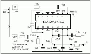
The TBA120 Series ICs provide a high-gain limiting IF amplifier and a quadrature coincidence detector in one package. These ICs are primarily intended for extraction of TV intercarrier sound, which (in Europe) is frequency modulated onto a 5.5MHz or 6MHz subcarrier. The TV waveform constitutes an extreme interfering signal, and the TBA120 provides superior performance in comparison to early Foster-Seeley and Ratio Detector systems, with a considerable reduction in component count.
TBA120 as AM demodulator. Equivalents are SN76660N (TI) and S041P (the latter is a low power version). It is in fact a CW/SSB/AM-multimode-detector, but the BFO line is connected to the signal from the IF. Believe I tested it in my Drake 2-B. Please note that TBA120AS, TBA120S, TBA120C, TBA120D etc are different and may not function satisfactorily in this construction. It is also suggested the change for use as SSB detector,but it is an old device and the circuit has more interest as a reference IF level is supposed to be maximum 50mV RMS. MC1351 should not have more than 10-20mV, and TDA1576 is overloaded with higher levels than 100mV RMS. NE/SA604/614 could also well be used, but have not been tested.
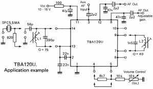
The TBA120U is an i.f. amplifier with a symmetrical FM demodulator and an a.f. amplifier with adjustable output voltage. The a.f. amplifier is also provided with an output for volume control and an input for VCR operation.
TBA120 demodulator circuit wiring diagram
The input and output of the TBA120U are especially designed for LC-circuits, but the input can also be used with a ceramic filter.
TBA120U demodulator
(View)
View full Circuit Diagram | Comments | Reading(3711)
Touch controlled musical bell
Published:2012/10/11 2:23:00 Author:muriel | Keyword: Touch controlled, musical bell
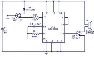
This touch controlled musical bell circuit circuit produces a musical tone whenever someone touches the touch point designated as TP in the circuit. The circuit works from two AA cells and produces enough sound.The circuit uses IC UM 3481 commonly used in musical circuits. The IC contains a ROM with 512 musical notes, tone generator, rhythm generator, modulator, run off control, oscillators, frequency divider and preamplifiers,. So a very few number of components is required for this circuit.C1 and R1 act as the timing components for the built in oscillator. The transistor Q1 is used for driving the loud speaker. The base of the transistor Q2 is used as the touch point to trigger the musical bell.
Touch musical bell circuit diagram
(View)
View full Circuit Diagram | Comments | Reading(1946)
Adjustable Variable power supply
Published:2012/10/11 2:22:00 Author:muriel | Keyword: Adjustable Variable, power supply
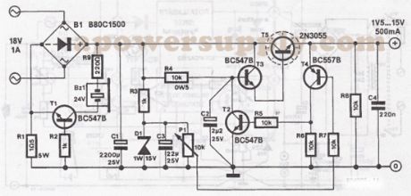
aPowerSupply.com has published a good variable power supply circuit schematic which can be adjusted between 1,5 V and 15 V with a 500 mA maximum current.It uses the well known 2N3055 transistor in a Darlington configuration.
Adjustable power supply circuit diagram
(View)
View full Circuit Diagram | Comments | Reading(1458)
LM7805 voltage regulator
Published:2012/10/11 2:22:00 Author:muriel | Keyword: LM7805, voltage regulator

Voltage regulator IC’s, with 3 pins, from LM7805 and LM7812 series are excellent for usage in voltage regulator circuits. If you need higher currents, up to 3 A, you must add a complementary transistor, T2 in this schematic. In a normal design, in case of a shortcircuit, the power dissipation can be very high. This problem can be solved using the voltage regulator design presented on aPowerSupply.com – voltage regulator circuit.
7805 voltage regulator circuit diagram
(View)
View full Circuit Diagram | Comments | Reading(5282)
AGC circuit = Automatic gain control
Published:2012/10/11 2:22:00 Author:muriel | Keyword: AGC circuit
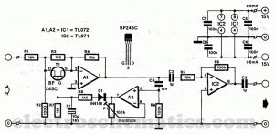
The automatic gain control circuit AGC provides a signal with less harmonics and additional amplification, between certain limits.As a result, it eliminates those intensity differences, annoying, and of speech music, which sometimes appear on radio and television.Field effect transistors T1 is used as a variable resistance. It’s value can vary from infinity to about 150Ω. It is in parallel with R3 and R4 together with, inducing the amplification of A1. Without FET, gainof A1 is about 20 dB.
AGC Automatic Gain Control circuit diagram
Amplification of A1 and A2 compensates damper losses: total agc circuit gain, with T1 blocked is 0 dB. Signals with a level lower than that set by P1 are amplified by a factor of maximum of 6.9 (= 17 dB amplification).
AGC components list semiconductors
D1 = 1N4148T1 = BF245CIC1 = TL072IC2 = TI071
Automatic gain control PCB
(View)
View full Circuit Diagram | Comments | Reading(3325)
Stereo switch circuit
Published:2012/10/11 2:21:00 Author:muriel | Keyword: Stereo switch
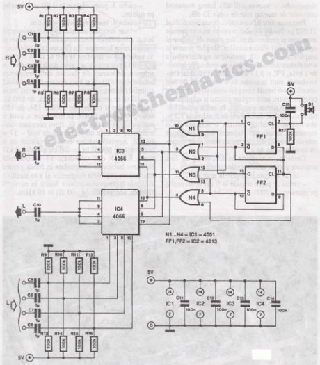
This stereo audio switch circuit allows that with only one switch to select one of the four stereo channels. The internal switching is made posible with CMOS components.
Each switch input includes a voltage divider to allow the switch to work in the linear zone of the characteristics, this ensures low audio signal distorsions.
Through the stereo switch circuit will flow a 1 mA current intensity at 5V. This voltage can be increased up to 15V.
Stereo audio switch circuit diagram
(View)
View full Circuit Diagram | Comments | Reading(1100)
FM antenna booster circuit
Published:2012/10/11 2:21:00 Author:muriel | Keyword: FM, antenna booster
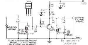
This is a low cost fm antenna booster that can be used to listen to programmes from distant FM stations clearly. The antenna fm booster circuit comprises a common-emitter tuned RF preamplifier wired around VHF/UHF transistor 2SC2570 (C2570).Assemble the circuit on a good-quality PCB (preferably, glass-epoxy). Adjust input/output trimmers (VC1/VC2) for maximum gain.
Input coil L1 consists of four turns of 20SWG enamelled copper wire (slightly space wound) over 5mm diameter former. It is tapped at the first turn from ground lead side. Coil L2 is similar to L1, but has only three turns. Pin configuration of transistor 2SC2570 is shown in the fm antenna booster schematic.
FM antenna booster circuit diagram
(View)
View full Circuit Diagram | Comments | Reading(1860)
1W fm transmitter circuit
Published:2012/10/11 2:20:00 Author:muriel | Keyword: 1W, fm transmitter

A very good 1 watt fm transmitter circuit, very easy to build circuit. It has 4 transistors, one is a very stable oscillator, followed by a buffer stage to prevent frequency variation when you adjust the transmitter. Next is a resonance stage and the final stage built with a minimum 1W transistor which must have a heatsink. You must use a LM7805 stabilizer for the oscillator diodes and one LM7809 for powering up the T1 oscillator stage. This will give you a very stable transmitter frequency.
1W FM Transmitter Circuit Diagram
First build the oscillator stage and the buffer, power it up and trim the 10k linear potentiometer untill you can here a blank signal on your receiver. If you put a small piece of wire on the T2 emitter you can see that the cover range of the 2 stage transmitter is about 3 meter.
After you are sure that your oscillator+buffer stage are working properly, remove the power supply and continue building the T3 resonance stage. Connect the power supply and if you adjust the trimmer (variable capacitor) from T3 collector you can see how the fm transmitter power can be varied. This stage is very important for proper functionality of the entire 1 watt fm transmitter. You must adjust the trimmer for maximum power.
1 Watt fm transmitter adjustment
The final stage of the 1W fm transmitter is built with 2N4427 (recommended) or the transistors from the list. If you can’t find any, use a BD139 transistor but only for frequencies lower than 90 MHz. The output power will be lower but you get the idea. If you decide to use 2N2219 transistor for the final stage of the transmitter you must know that the output rf power will be 0.4W.
Adjust the last 2 trimmers for maximum output power in the antenna. Initially use 2 x 100 Ω 0.5W resistors in parallel at the RF output. Then connect this rf probe to the output and adjust all the 3 trimmers starting from T3 to output. You must adjust it to obtain the maximum multimeter indication. Then power it off, connect the antenna and make the final adjustments for maximum broadcasting coverage distance.
The oscillator and buffer stage must be enclosed in a 1 mm copper case, then do the same with the T3 and T4 stages.
Use a 12Vdc power supply to power up this fm broadcast circuit. T4 will have a current consumption of around 150 mA at full power output adjustments. The total current consumption of the entire 1 watt transmitter will be around 500 mA. (View)
View full Circuit Diagram | Comments | Reading(1546)
The control alarm circuit with SGZ07 sound and light alarm integrated circuit
Published:2012/10/10 22:04:00 Author:Ecco | Keyword: control alarm , sound and light, alarm, integrated circuit
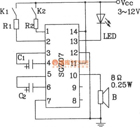
In the figure, the on-off of K1 the K2 allow the circuit to work in dual-band sound, light alarm circuit. If the R1, R2 of circuit are replaced by the corresponding thermistors ( measured value), it can realize the temperature control alarm circuit.
(View)
View full Circuit Diagram | Comments | Reading(1103)
Power status indicator circuit
Published:2012/10/10 21:45:00 Author:Ecco | Keyword: Power status, indicator
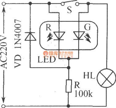
As shown in the figure, LED - R is used for power source directions, LED-G is used for working condition indicator of the load HL ( lamp ). When 220V AC mains is normal, LED - R emits red light. When switch S is closed, HL also emitting light, LED-G emits green light, because the LED-R also emits light at this time, bicolor LED emits orange-red light when S is closed.
(View)
View full Circuit Diagram | Comments | Reading(2133)
| Pages:307/2234 At 20301302303304305306307308309310311312313314315316317318319320Under 20 |
Circuit Categories
power supply circuit
Amplifier Circuit
Basic Circuit
LED and Light Circuit
Sensor Circuit
Signal Processing
Electrical Equipment Circuit
Control Circuit
Remote Control Circuit
A/D-D/A Converter Circuit
Audio Circuit
Measuring and Test Circuit
Communication Circuit
Computer-Related Circuit
555 Circuit
Automotive Circuit
Repairing Circuit