
Circuit Diagram
Index 301
How to build Economy radar detector
Published:2012/10/18 3:22:00 Author:muriel | Keyword: Economy, radar, detector
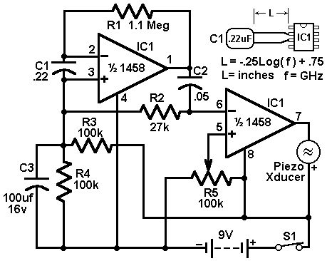
This circuit uses a 1458 dual op-amp to form a radar detector. C1 is the detector of the radar signal. The first op-amp forms a current-to-voltage converter and the second op-amp buffers the output to drive the piezo transducer. R5 sets the switching threshold of the second op-amp; normally it is adjusted so that the circuit barely triggers on background noise, then it's backed off a bit. The response of the circuit may be tuned by adjusting the length of the leads on C1. For typical road-radar systems, the input capacitor's leads should be about 0.5 to 0.6 inches long. (View)
View full Circuit Diagram | Comments | Reading(2745)
Digital Radar| Speedometer
Published:2012/10/18 3:20:00 Author:muriel | Keyword: Digital Radar, Speedometer
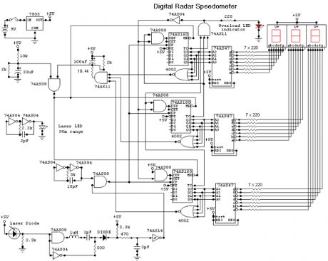
This circuit is a Digital Radar Speedometer. It allows us to evaluate the speed of any object moving, especially cars and other vehicles. The speed is calculated in kilometers per hour (KPH). Its display has three digits. This radar works with the laser reflexion. It sends laser radiation to the object and this object reflects the laser radiation to the radar. To evaluate the speed of a vehicle, we must be in front of it. In other words, the vehicle must come in our direction. The front of the radar must point the front of the vehicle. The radar has the shape of a pistol. In this radar, it has a laser LED and a laser diode. Both have a lens.
The laser LED can send a spot of light to a distance of 90 m (295 ft). It's very important that the distance range of the laser LED is 90 m, if not, the speed will not be calculated properly. The laser diode, which receives the light signal by the laser LED, must be able to detect the light which is same color as that emitted by the laser LED. The laser diode and the laser LED must be placed one beside the other. They are protected by a tinted pane. They must be placed at the front of the radar and point the outside. The radar is powered by a 9V battery and it has a SPST switch to control its power state.
The display, or the speed indicator, is placed at the rear of the radar, just on the right of the overload LED indicator. All the logic components of the circuit must be of the 74AS series and TTL type. Because they have short time of response (less than 1.7 ns) and have high frequency supports (more than 200 MHz). The radar can evaluate the speed of an object moving between 0 to 999 km/h. After this speed, the overload LED indicator will turn on and the 999 will still displayed. The radar displays the speed during 3 seconds, after this time, it displays zero (0). (View)
View full Circuit Diagram | Comments | Reading(1628)
CMOS SCHMITT TRIGGER IC
Published:2012/10/18 3:18:00 Author:muriel | Keyword: CMOS, SCHMITT , TRIGGER IC
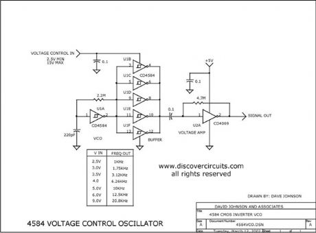
By changing the supply voltage fed to a classic 4584 Schmitt trigger type oscillator, the oscillator frequency can be changed over a range of 50:1. A 74HCU04 inverter is used at the output of the 4584 to maintain a constant TTL logic level signal. (View)
View full Circuit Diagram | Comments | Reading(2760)
Miniature Audio Oscillator
Published:2012/10/18 3:16:00 Author:muriel | Keyword: Miniature , Audio, Oscillator
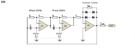
The oscillator circuit (see Figure 1) involves two unity gain phase shift stages, A1 and A2, in tandem and a gain stage, A3, with back to back diodes and resistor network providing non-linear negative feedback. At a particular frequency (determined by RT and CT - the timing components) A1 and A2 provide 90 degrees phase shift each, 180 degrees in total and the circuit begins oscillating, since A3 and its non linear network has more than unity gain for small signals. As the oscillation level increases the diodes conduct and limit the gain of A3 stabilising the output at the desired level, in this case a little over 1V RMS. However, some distortion of the sine wave peaks is caused by the diodes. (View)
View full Circuit Diagram | Comments | Reading(1291)
Microphone Mixer
Published:2012/10/18 3:15:00 Author:muriel | Keyword: Microphone, Mixer
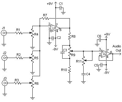
This relatively simple mixer was designed for three dynamic microphones, but can be re-designed for more or less. Level and tone controls are available to tailor the sound to your needs.
(View)
View full Circuit Diagram | Comments | Reading(2853)
Simple line mixer
Published:2012/10/18 3:14:00 Author:muriel | Keyword: Simple line, mixer

I designed this circuit for one friend of mine to be used as a small portable DJ mixer. The circuit is an audio mixer circuit so simple as it can be. There are two dual logarithmic potentiometers in the circuit to adjust the input signal levels and some resistors to do the actual mixing. The circuit is totally passive, so no power supply is needed.
The circuit is suitable to be uses as a mixer between two line level sources and one HIFI amplifier input. This circuit have been successfully used for mixing signals form two CD players or computer soundcard and CD players. There are many situations where simple mixer would be useful and commercially available mixer desks are too expensive and big.
This simple line mixer has two drawbacks: it attenuates the signal all the time (even sliders set to maximum) and the output impedance is quite high. The first problem can be solved by just turning a little more volume in the amplifier. High ouput impedance is no problem when connected to high impedance amplifier input with short wires (few meters).
In the picture below you see the schematic of the whole mixer circuit. The potentiometer slides which are actually inside one dual potentiometers are connected together using one line. Every input and output pin has corresponding ground signal on the right side of the signal line.
(View)
View full Circuit Diagram | Comments | Reading(1311)
FET Audio Mixer
Published:2012/10/18 2:29:00 Author:muriel | Keyword: FET, Audio, Mixer
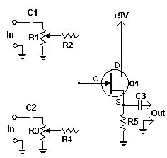
This simple circuit mixes two or more channels into one channel (eg. stereo into mono). The circuit can mix as many or as few channels as you like and consumes very little power. The mixer is shown with two inputs, but you can add as many as you want by just duplicating the sections which are clearly visible on the schematic.
(View)
View full Circuit Diagram | Comments | Reading(1488)
Simplest Ever Amplifier Bridging
Published:2012/10/18 2:28:00 Author:muriel | Keyword: Simplest Ever, Amplifier

In another of my project pages, there is a design for a simple add-on bridging adapter for stereo power amplifiers. There is, however, an even simpler way, provided you have (or can trace out) the appropriate section of the amplifier circuit.
Nearly all modern amplifiers use a long-tailed pair as the input and error amplifier (the error amp is the LTP, which detects any variation between its inputs - an error voltage - and corrects it). The input is connected to the base of one of the LTP transistors, and the feedback to the other. The feedback signal is attenuated by the network, by an amount equal to the gain of the amplifier.
By connecting the output of one amplifier to the feedback point in the other, using a resistance equal to that for the feedback resistor, the second amp will have a signal gain of unity, and will be inverted, since the feedback is always applied to the inverting input. (View)
View full Circuit Diagram | Comments | Reading(1803)
Audio Voice-Over Circuit
Published:2012/10/18 2:27:00 Author:muriel | Keyword: Audio, Voice-Over Circuit
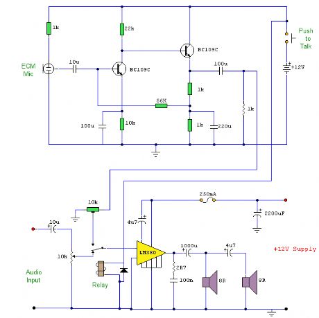
This is a circuit where a microphone and preamp circuit (voice circuit) have priority over any other audio signal. You can think of this as a one way intercom, if the main amplifier is used for listening to music, then when the push to talk switch is pressed, the amplifier is switched to the voice signal.
(View)
View full Circuit Diagram | Comments | Reading(1968)
Audio Signal Source
Published:2012/10/18 2:26:00 Author:muriel | Keyword: Audio, Signal Source
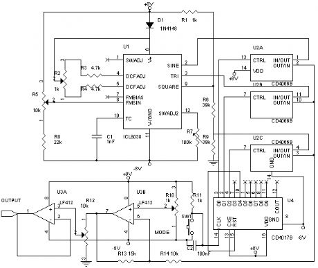
The circuit shown below can be roughly divided into three parts: the oscillator based around the ICL8038 chip, the selection logic based on the CD4017 and CD4066 and the offset generation and output buffers, based on the LF412. Apologies for the cramped schematic, I had to keep the image size small, and the width under 640 pixels!
The oscillator is a standard 8038-based oscillator circuit, taken from the ICL8038 datasheet. The timing resistor chosen is rather small, to give a wide range of frequencies. This range might be a little too large, making precise frequency setting difficult. In that case, the freqency range may be split into two parts, using two capacitors which can be switched using an SPDT switch. Note that the 8038 is powered from a split supply, not a single supply, to generate a symmetrical waveform without the need for capacitor coupling. Two sine wave adjustment terminals (Pins 1 and 12) are provided, however only one is used. This gives a sinewave distortion of about 1%. To achieve better distortion figures, the circuit shown in Figure 4 of the ICL8038 datasheet may be used. The 8038 is powered from slightly less than +8V to allow the tuning voltage to go above the supply rail. This allows for maximum sweep range (1000:1), however the output waveform tends to be slightly asymmetric because of this. This may be compensated using the offset control R10. R2 controls the duty cycle of the oscillator. R7 acts as the sinewave distortion adjustment. The square wave output of the 8038 is an open-collector output. Hence, a 1k pullup resistor is provided. The sine and triangle outputs are about 5Vpp, while the square wave is 16Vpp. Hence to equalize the different outputs, the square wave is attenuated using a fixed attenuator formed by R6 and R9. A 47k pot may be substituted to make the attenuation level adjustable. (View)
View full Circuit Diagram | Comments | Reading(2145)
3 lines mixer
Published:2012/10/18 2:25:00 Author:muriel | Keyword: 3 lines, mixer
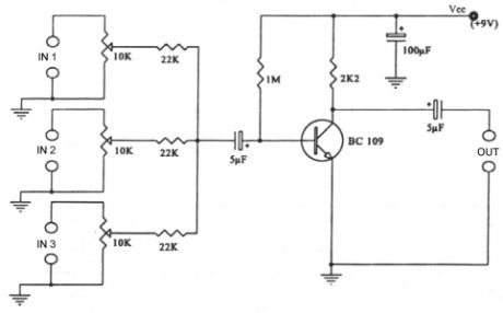
This project is a 3 or more lines mixer. For more than 3 inputs you can repeat the input parts (P=10K R=22K). It powered with 9Vdc.
(View)
View full Circuit Diagram | Comments | Reading(860)
LED| Photo Sensor.
Published:2012/10/18 2:16:00 Author:muriel | Keyword: LED, Photo Sensor
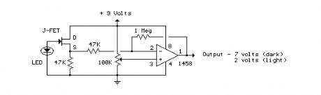
Here's a circuit that takes advantage of the photo-voltaic voltage of an ordinary LED. The LED voltage is buffered by a junction FET transistor and then applied to the inverting input of an op-amp with a gain of about 20. This produces a change of about 5 volts at the output from darkness to bright light. The 100K potentiometer can be set so that the output is around 7 volts in darkness and falls to about 2 volts in bright light.
(View)
View full Circuit Diagram | Comments | Reading(1756)
Triangle and Squarewave Generator
Published:2012/10/18 2:15:00 Author:muriel | Keyword: Triangle, Squarewave, Generator
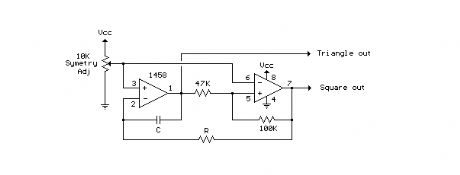
Here is a simple triangle/squarewave generator using a common 1458 dual op-amp that can be used from very low frequencies to about 10 Khz. The time interval for one half cycle is about R*C and the outputs will supply about 10 milliamps of current. Triangle amplitude can be altered by adjusting the 47K resistor, and waveform offset can be removed by adding a capacitor in series with the output.
(View)
View full Circuit Diagram | Comments | Reading(1115)
Low Frequency Sinewave Generators
Published:2012/10/18 2:09:00 Author:muriel | Keyword: Low Frequency, Sinewave Generators
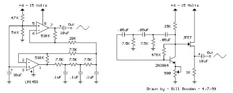
The two circuits below illustrate generating low frequency sinewaves by shifting the phase of the signal through an RC network so that oscillation occurs where the total phase shift is 360 degrees. The transistor circuit on the right produces a reasonable sinewave at the collector of the 3904 which is buffered by the JFET to yield a low impedance output. The circuit gain is critical for low distortion and you may need to adjust the 500 ohm resistor to achieve a stable waveform with minimum distortion. The transistor circuit is not recommended for practical applications due to the critical adjustments needed.
The op-amp based phase shift oscillator is much more stable than the single transistor version since the gain can be set higher than needed to sustain oscillation and the output is taken from the RC network which filters out most of the harmonic distortion. The sinewave output from the RC network is buffered and the amplitude restored by the second (top) op-amp which has gain of around 28dB. Frequency is around 600 Hz for RC values shown (7.5K and 0.1uF) and can be reduced by proportionally increasing the network resistors (7.5K). The 7.5K value at pin 2 of the op-amp controls the oscillator circuit gain and is selected so that the output at pin 1 is slightly clipped at the positive and negative peaks. The sinewave output at pin 7 is about 5 volts p-p using a 12 volt supply and appears very clean on a scope since the RC network filters out most all distortion occurring at pin 1.
(View)
View full Circuit Diagram | Comments | Reading(1118)
Low Frequency Wien Bridge RC Sinewave Oscillators
Published:2012/10/18 2:08:00 Author:muriel | Keyword: Low Frequency, Wien Bridge , RC Sinewave , Oscillators
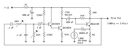

Three examples of Wien Bridge oscillators are shown below. The first uses three bipolar transistors. The second uses a bipolar and JFET, and the third is the more popular type using an op-amp for minimal parts. The idea is to generate a 360 degree phase shift at some particular frequency using 2 resistors and caps of equal value. One cap and resistor are in series, while another cap and resistor are in parallel. The signal loss through the network is about 66 percent so the amplifier gain needs to be around 3 for a loop gain of 1. The gain of the amplifier is critical since too much gain will produce a clipped (distorted) waveform and not enough gain will not sustain oscillation. This is almost impossible to achieve without some automatic gain control (AGC) to regulate the gain and produce stable operation. The usual AGC is accomplished with a small light bulb where resistance increases as the signal level rises and reduces the gain. The lamp used here is a 1819 (28 volt 40mA) variety found at Radio Shack, part number 272-1119. Another lamp that might be useful is the GE394, 12 volt 40mA, but a little harder to find.
In the first example, the lamp is placed in series with a 1000uF cap and connected across the emitter resistor of the 2N2219A so as the signal level rises, the total resistance increases reducing the gain. The gain of the 2N2219A stage is approximately the collector resistor (100) divided by the emitter resistor (51 in parallel with the lamp 75) or maybe 100/30 = 3.3, The first stage (2N3904 on the left) provides a high impedance to the RC network so it doesn't load down the input much. The second stage (2N3904) in the middle, provides a 180 degree phase inversion and not much voltage gain. So, the overall phase shift is 360 degrees, 180 from the middle stage and another 180 from the 2N2219A stage. The overall gain can be adjusted with the 750 ohm resistor at the collector of the center stage. The example shows 2 (20K) variable resistors which are ganged together for frequency adjustment of about 10KHz to 400 Khz. Lower frequencies can be obtained using larger capacitors. The frequency of oscillation is f = 1/(2 * Pi * R * C). The circuit was built sucessfully and also simulated using LTSpice version IV. A copy of LTSpice can be downloaded from the following link. (View)
View full Circuit Diagram | Comments | Reading(2367)
Touch Activated Light
Published:2012/10/18 2:07:00 Author:muriel | Keyword: Touch, Activated Light
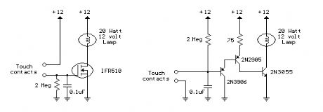
The circuits below light a 20 watt lamp when the contacts are touched and the skin resistance is about 2 Megs or less. The circuit on the left uses a power MOSFET which turns on when the voltage between the source and gate is around 6 volts. The gate of the MOSFET draws no current so the voltage on the gate will be half the supply voltage or 6 volts when the resistance across the touch contacts is equal to the fixed resistance (2 Megs) between the source and gate.
The circuit on the right uses three bipolar transistors to accomplish the same result with the touch contact referenced to the negative or ground end of the supply. Since the base of a bipolar transistor draws current and the current gain is usually less than 200, three transistors are needed to raise the microamp current level through the touch contacts to a couple amps needed by the light. For additional current, the lamp could be replaced with a 12 volt relay and diode across the coil. (View)
View full Circuit Diagram | Comments | Reading(1200)
AC Line Current Detector
Published:2012/10/18 2:06:00 Author:muriel | Keyword: AC, Line Current, Detector
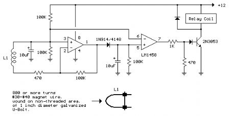
This circuit will detect AC line currents of about 250 mA or more without making any electrical connections to the line. Current is detected by passing one of the AC lines through an inductive pickup (L1) made with a 1 inch diameter U-bolt wound with 800 turns of #30 - #35 magnet wire. The pickup could be made from other iron type rings or transformer cores that allows enough space to pass one of the AC lines through the center. Only one of the current carrying lines, either the line or the neutral should be put through the center of the pickup to avoid the fields cancelling. I tested the circuit using a 2 wire extension cord which I had separated the twin wires a small distance with an exacto knife to allow the U-bolt to encircle only one wire.
The magnetic pickup (U-bolt) produces about 4 millivolts peak for a AC line current of 250 mA, or AC load of around 30 watts. The signal from the pickup is raised about 200 times at the output of the op-amp pin 1 which is then peak detected by the capacitor and diode connected to pin 1. The second op-amp is used as a comparator which detects a voltage rise greater than the diode drop. The minimum signal needed to cause the comparator stage output to switch positive is around 800 mV peak which corresponds to about a 30 watt load on the AC line. The output 1458 op-amp will only swing within a couple volts of ground so a voltage divider (1K/470) is used to reduce the no-signal voltage to about 0.7 volts. An additional diode is added in series with the transistor base to ensure it turns off when the op-amp voltage is 2 volts. You may get a little bit of relay chatter if the AC load is close to the switching point so a larger load of 50 watts or more is recommended. The sensitivity could be increased by adding more turns to the pickup. (View)
View full Circuit Diagram | Comments | Reading(1934)
Input current protection circuit diagram using INA321/322
Published:2012/10/17 21:14:00 Author:Ecco | Keyword: Input current , protection
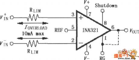
INA321/322 input end's interior has electrostatic discharge (ESD) protection diode, and the protection diode will get conduction when the input voltage exceeds the supply voltage 500mV, then RLIM will limit the input current ( 10mA ) to play a role in the protection circuit. Many input signals have limited streaming capabilities, at the time, the current limiting resistor RLIM can be ignored.
(View)
View full Circuit Diagram | Comments | Reading(804)
The LM317T application circuit diagram
Published:2012/10/17 21:53:00 Author:Ecco | Keyword: application
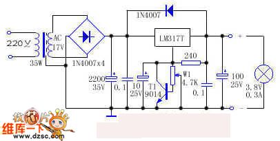
It uses LM317T to make adjustable power supply, but the problem is that the load is often burned due to poor contact of potentiometer and output voltage increases. If the circuit increases a transistor, under normal circumstances, the base potential of T1 is 0, and T1 is cut off, and it has no effect on the circuit; when W1 is in poor contact, the base of T1 electrode potential rises, when it is raised to 0.7V, T1 gets conduction to reduce LM317T adjustment terminal voltage, then the output voltage is also reduced, thereby to play a protective role on the load.
(View)
View full Circuit Diagram | Comments | Reading(5448)
Commonly used simple oscillator circuit diagram
Published:2012/10/17 22:16:00 Author:Ecco | Keyword: oscillator
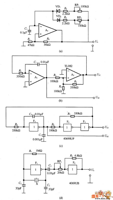
Figure (a) is the square wave output circuit, in the circuit, the op amp A1 is added a positive feedback, i.e., feedback resistor R2 is connected between the noninverting input and output terminals to form a comparator circuit with the delay characteristics. The voltage on R1 and the charging and discharging voltageof capacitor C1 cause oscillation from comparison. High and low level time of output square wave can be set independently, and the oscillation frequency is determined by the high and low level time, namely, it uses diodes VD1 and VD2, potentiometer RP1 and RP2 to set the charging and discharging time of capacitor C1.
(View)
View full Circuit Diagram | Comments | Reading(1418)
| Pages:301/2234 At 20301302303304305306307308309310311312313314315316317318319320Under 20 |
Circuit Categories
power supply circuit
Amplifier Circuit
Basic Circuit
LED and Light Circuit
Sensor Circuit
Signal Processing
Electrical Equipment Circuit
Control Circuit
Remote Control Circuit
A/D-D/A Converter Circuit
Audio Circuit
Measuring and Test Circuit
Communication Circuit
Computer-Related Circuit
555 Circuit
Automotive Circuit
Repairing Circuit