
Circuit Diagram
Index 312
USB Cellphone Charger circuit
Published:2012/10/8 2:47:00 Author:muriel | Keyword: USB, Cellphone Charger
Now you can charge your Mobile Phone from the USB outlet of PC. This simple usb cellphone charger circuit can give regulated 4.7 volts for charging the mobile phone. USB outlet can give 5 volts DC and 100 mA current which is sufficient for the slow charging of mobile phones.
USB Cell Phone Charger Circuit Schematic
Most of the Mobile Phone battery is rated 3.6 volts at 1000 to 1300 mAh. These battery packs have 3 NiMh or Lithium cells having 1.2 volt rating. Usually the battery pack requires 4.5 volts and 300-500 mA current for fast charging. But low current charging is better to increase the efficiency of the battery. The circuit described here provides 4.7 regulated voltage and sufficient current for the slow charging of the mobile phone.
Transistor T1 is used to give the regulated output. Any medium power NPN transistor like CL100, BD139, TIP122 can be used. Zener diode ZD controls the output voltage and D1 protects the polarity of the output supply. Front end of the circuit should be connected to a A type USB plug. Connect a red wire to pin1 and black wire to pin 4 of the plug for easy polarity identification. Connect the output to a suitable charger pin to connect it with the mobile phone. After assembling the circuit, insert the USB plug into the socket and measure the output from the circuit. If the output is OK and polarity is correct, connect it with the mobile phone.
Note: If the polarity is incorrect, it will destroy the cellphone battery. So take extreme care. (View)
View full Circuit Diagram | Comments | Reading(1517)
Flashing Brake Light for Motorcycles circuit
Published:2012/10/8 2:47:00 Author:muriel | Keyword: Flashing, Brake Light
This flashing brake light circuit can be used for motorcycles. When brake-light switch S1 is closed, power is applied to U1 and U2. Two inverters of U2, a 4049 hex inverting buffer, are connected in a low frequency oscillator that feeds clock pulses into U1, a 4017 decade counter/divider. Outputs 0, 2, 4, 6 and 8 of U1 are coupled to the gate of Q1 through a 1N914 diode.As the 4017 counts, it turns the brake light on and off four times and then leaves it on until the brake switch is released. The on/off rate can be set by potentiometer R2.For best results, the on/off rate should be set so that it is rapid.
Flashing Brake Light Circuit Diagram
(View)
View full Circuit Diagram | Comments | Reading(1360)
Electronic Bicycle Horn circuit
Published:2012/10/8 2:46:00 Author:muriel | Keyword: Electronic Bicycle, Horn
This simple electronic bicycle horn circuit uses only one gate of a 4093 quad 2-input NAND Schmitt trigger, U1, conected in a simple, low frequency, square-wave oscillator circuit.The oscillator’s output, at pin 3, drives the gate of Q1. The drain of that FET drives a small horn speaker.
Potentiometer R1 can be adjusted to set the horn’s output frequency. Some horn speakers are frequency sensitive, so play with the oscillator’s frequency control for the best loudest sound.
Electronic Bike Horn Circuit Diagram
(View)
View full Circuit Diagram | Comments | Reading(1422)
Triangle Waveform Generator circuit with 555
Published:2012/10/8 2:45:00 Author:muriel | Keyword: Triangle Waveform, Generator circuit,555
The circuit is a triangle waveform generator that uses as few parts as possible.A 555 timer IC, 2 resistors and two capacitors make the triangle wave.The IC is connected in a 50% duty-cycle astable square-wave oscillator circuit.The square-wave output is fed from pin 3 of the IC to an RC shaping circuit.When the 555′s square-wave output goes high, C2 begins to charge through R2 and the voltage across C2 increases as long as the output remains high. When the IC’s output goes low again, C2 begins to discharge through R2 reducing the voltage C2 as long the output remains low. The resulting waveform accross C2 takes the shape of a triangle. The best waveform linearity is obtained when R2 and C2 are made as large as possible. With the component values shown, the peak-to-peak output is 0.5 V at a frequency of about 200 Hz.
Triangle Waveform Generator Circuit Diagram
(View)
View full Circuit Diagram | Comments | Reading(1355)
Mobile Scanner Circuit
Published:2012/10/8 2:45:00 Author:muriel | Keyword: Mobile Scanner
Here is a device to locate the mobile phone. It emits intermittent flashes and beeps to indicate the presence of an active mobile phone. The circuit becomes active even if the mobile phone is in silent mode. It can be used to detect mobile phone call in noisy environments. Range of the circuit is 15 cm.The circuit is basically an RF detector. During the activation of mobile phone, strong RF field will be generated. The sensor coil L detects the RF signals and T1 amplifies the signals. The amplified signals are given to the clock input of IC1. CD 4017 is a Johnson decade counter IC with 10 outputs. Its clock input pin 14 is highly sensitive to RF pulses so that it is a very good choice for RF detection. Only two outputs (Q1 andQ2) of the IC are used while the Q3output is tied to the reset pin 15 so that IC will reset on every third pulse.
This will repeat the activation of LED and Buzzer. When the sensor detects the RF signal, clock input of IC1 gets pulses and its output pins 2 and 4 becomes high and low alternately giving flashing lights and beeps. The coil used in the circuit is a ready made inductor.Buzzer used is a small piezo buzzer.
Mobile Scanner Circuit diagram
(View)
View full Circuit Diagram | Comments | Reading(1936)
Electronic Dice circuit
Published:2012/10/8 2:44:00 Author:muriel | Keyword: Electronic Dice
With this electronic dice the result is displayed with LEDs that are placed so every dice face is shown. In the circuit diagram, IC 4022 is used to count to 6 in which only one output can get “1″ state.A diode matrix (D1..D8) serve as decoding the output signals of the counter so that the LEDs are controlled by two buffer transistors and series resistance.Integrated circuit outputs only support a reduced load, so in the transistor’s base are connected the limiting resistances. As a clock generator it can be used any generator with rectangular pulses whose amplitude corresponds to the IC’s supply voltage. The 4022 clock input impedance is 1012Ω.
Electronic Dice Circuit Diagram
(View)
View full Circuit Diagram | Comments | Reading(747)
Flashing Light with Triacs
Published:2012/10/8 2:43:00 Author:muriel | Keyword: Flashing Light
This flashing light circuit uses triacs to generate an intermittent light with variable frequency. Additional components are the D1 diode and semi adjustable potentiometer R2. The trigger capacitor C1 is increased from 0.1 µF to 220 µF so that the triacs can be ordered for several successive periods. C1′s loading time is longer, so that the lamp flashes with one pause of several periods.Blinking frequency can be adjusted with P1. Semi-adjustable potentiometer R2 regulates the current gate. This setting affects the lighting duration of the lamp because it also establish the C1′s discharging time.
Triac Flashing Light Circuit Diagram
(View)
View full Circuit Diagram | Comments | Reading(1373)
Car DC Adapter circuit
Published:2012/10/8 2:43:00 Author:muriel | Keyword: Car, DC Adapter
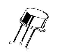
Here is a DC adapter to charge Mobile phone or play a Music system using the power from car battery. The adapter will provide 4.7 volt regulated DC from the 13.5 volt DC power of the car battery. The circuit is basically a DC to DC converter with voltage and current regulation. The 13.5 volt DC from the car battery is given to the collector and base of T1. R1 restricts the base current of T1 to a safer level so that output will be current regulated. T1 is an NPN Darlington transistor so that its high gain gives maximum output current. Diode D1 protects the circuit from accidental polarity reversal during connections. By changing the value of ZD, it is possible to get required output voltage. Here the 4.7 volt zener gives regulated 4.7 volts for charging a mobile phone. The adapter can be plugged into the cigarette lighter outlet of the car dash board.It is better to give heat sinking to T1 to dissipate heat.
Car DC Adapter Circuit Diagram
TIP 122 Darlington Transistor
(View)
View full Circuit Diagram | Comments | Reading(957)
Traffic Alert Project
Published:2012/10/8 2:43:00 Author:muriel | Keyword: Traffic, Alert Project
This Solar based LED flasher can Alert vehicles in heavy traffic areas or places where road work is going on. It is fully automatic and turns on in the evening. During day time it remains off and charge the battery using solar energy.The circuit has two sections. A battery charger and a Flasher circuit. The battery charger uses 6 volt solar panel to convert light energy into electrical energy. During day time, the fully illuminated solar panel provides 6 volts DC through diode D1 to charge battery. When current flows through D1, base of the PNP Darlington transistor T1 remains positive to keep it off. So the flasher section will not get current and it remains off. When the light falling on the solar panel reduces, current flow through D1 ceases and it reverse biases. T1 then conducts as its base becomes negative. This provides current to the flasher circuit.
Flasher circuit is built around the popular binary counter IC HEF4060. A CMOS version is used to reduce the power consumption. When the IC gets battery power supply from the collector of T1, it resets through C1 and R2 and starts oscillations using R4 and C2. Out put pulses will be available from the Q3 output (pin7) causing T2 to turn on/off alternately. This makes the LED string flashing.
Modifications
The circuit is designed for six LEDs using a miniature 4.8 volt rechargeable battery. If more LEDs are required, increase the value of solar panel to 12 volts and the capacity of battery to 6 volt 4.5Ah. Use High bright transparent yellow LEDs for more visibility. For portable use, fix a switch in the battery positive.
Traffic Alert Circuit diagram
IC HEF4060
(View)
View full Circuit Diagram | Comments | Reading(754)
USB Reading Lamp circuit
Published:2012/10/8 2:43:00 Author:muriel | Keyword: USB, Reading Lamp
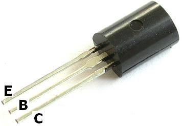
Light your table top with this cool White LED Lamp. It is powered from the USB port and is ideal to take notes while browsing internet. The USB port can provide 5 volts and 100 mA current which is sufficient to light the LED lamp.Power to the circuit is derived from the USB port using the standard A type plug. To give continuous regulated power, Zener regulation is employed. Resistor R1 restricts base current to T1 so that output will be current regulated. Since White LED requires minimum 3.6 volts, 4.7 volt Zener is used to provide constant 4.7 volts to LEDs. Resistor R2 restricts LED current to around 20 mA, so that they will not be damaged. Connect the power lines to USB plug observing correct polarity. Use a reflector for LEDs to get maximum illumination.
USB Reading Lamp Circuit diagram
Seetharaman observed that the current thru LEDs is too small, around 2 mA, so I have simulated this circuit and indeed there is only 4 mA for each LED. You may want to decrease the R2 value to 22Ω. I will build this on a
Pin out of SL 100
(View)
View full Circuit Diagram | Comments | Reading(1749)
Polyphonic DoorBell circuit
Published:2012/10/8 2:42:00 Author:muriel | Keyword: Polyphonic, DoorBell
Here is an AC triggered Multitone, polyphonic doorbell. It gives eight melodious tunes for 2 minutes. On each press it will give a new tone which will continue till the melody is over. The circuit is too simple and battery operated It uses the popular melody generator IC UM3481. The circuit uses the popular melody generator IC UM3481. It generates music tones like Jingle bell, Santa clause is coming, Silent night, Holy night, Joy to the world, Rudolph, Red nosed reindeer, Merry Christmas, O come, All Ye faithful, Hark and the herald angel sing.UM 3482 generates 12 music tones. Capacitor C1 and resistor R2 are the oscillation components. Pin1 can be triggered either by DC or AC. Here low voltage AC is applied to the trigger pin 1 through R1 and D1. The circuit works off two pen cells which last for more than one year
Caution: The circuit is connected to high volt AC. Do not touch any parts when it is powered to avoid lethal shock
Polyphonic DoorBell Circuit Diagram
UM 3481
AC187 Pinout
(View)
View full Circuit Diagram | Comments | Reading(1848)
Cupboard Lights circuit
Published:2012/10/8 2:42:00 Author:muriel | Keyword: Cupboard Lights
This Cupboard lights circuit is an automatic White LED lamp used to illuminate the interior of cupboard to search things. The lamp automatically turns on when the door of the cupboard opens and stays on for three minutes then turns off.The circuit uses the popular timer IC NE 555 for the time delay. Components R1 and C2 gives three minutes time delay during which the lamp remains on. Power to the circuit is obtained from a 9 volt PP3 battery. A magnetic reed switch is used for the automatic operation of the circuit. The Normally closed (NC) contacts of the reed switch break when the magnet is close to it if the door is closed. When the door opens, magnet move away and the contacts of reed switch closes and the circuit gets power. Since the trigger pin 2 of timer is grounded, timer triggers and its output become high to light the white LED lamp. Fix the reed switch and circuit in the frame of the cupboard and magnet in the door so as to keep them close when the door is closed.
Cupboard Light Circuit diagram
555 datasheet
IC NE 555 and Reed Switch
Pin connections of IC 555
(View)
View full Circuit Diagram | Comments | Reading(1259)
Anxiety Symptoms Generator
Published:2012/10/8 2:42:00 Author:muriel | Keyword: Anxiety Symptoms, Generator
Do you want to feel the anxiety symptoms or get rid of your guests?This circuit can be helpful when you want to get rid of your guests (visitors) or feel yourself how anxiety does it feel like. It is a frequency generator that generate a 14 Hertz hum that cannot be heard but will produce a strong anxiety feeling.In order to produce the restlessness you must connect this circuit to an audio amplifier in order to obtain enough sound pressure in the room to get the full impact.You can use the 47K potentiometer to adjust the output level on out 2.Don’t use this anxiety symptoms generator for a long period of time because the long-term effects have not been tested.
Anxiety Symptoms Generator Circuit Diagram
(View)
View full Circuit Diagram | Comments | Reading(847)
Radiation Sensor Circuit
Published:2012/10/8 2:41:00 Author:muriel | Keyword: Radiation Sensor
Here is a simple tool to check the degree of radiation from an electric or electronic instrument. The LEDs in the circuit will give a running light pattern at the moment the circuit senses electromagnetic radiation from the device. It can detect radiation from the Computer or TV from a distance of 2 feet or more.The speed of running light depends on the intensity of radiation. Fast running light indicates high amount of radiation and vice versa.IC CD4033 is the decade counter with7 segment display driver. It has seven outputs to drive LEDs or Seven segment display. The clock input (pin1) of IC is very sensitive and readily accepts energy from the electromagnetic radiation even from a long distance. This property of the IC CD4033 is exploited here to measure the intensity of radiation.The reset pin 15 of IC is connected to C1 and R1 to reset the IC after completing a cycle.So that the functioning of IC continues till the input pulses cease.
Areal
A small length plastic wire can be used as areal. A telescopic areal used in pocket radio will give an elegant look to the gadget
Test
Bring the areal close to the TV or CRT monitor of computer. All the LEDs light up one by one giving a running pattern. The speed of running light depends on the strength of radiation. Move away the unit from the monitor. As the diastance increases, speed of running light decreases. Finally all the LEDs stop glowing. This is the point without the radiation. Check all the electric instruments and mains wiring using the device and find out how much radiation is emitting.
Radiation Sensor Circuit diagram
CD4033
CRT Monitor
IC CD4033
(View)
View full Circuit Diagram | Comments | Reading(2128)
GigaHertz Signal Detector circuit
Published:2012/10/8 2:41:00 Author:muriel | Keyword: GigaHertz, Signal Detector
This circuit is useful to detect microwave (gigahertz signal) sources like microwave oven, satellite communication devices, Mobile phones etc. It gives audio visual indications when it detects the Microwaves in the Gigahertz band.Microwave is the form of EM radiation with frequencies between 2 GHz and 300 GHz. Microwave oven uses UHF around 3 GHz in the S band. Mobile phones and Satellite devices generally use 2 to 3.5 Gigahertz signals. The circuit exploits a few simple scientific facts about EM radiations and Magnetic induction. Electromagnetic radiation has both electrical and magnetic field components which oscillate in phase perpendicular to each other to the direction of energy propagation.
If an inductor coil with a parallel capacitor is placed in the path of EM radiation, the capacitor stores electrical energy and inductor stores energy in the magnetic field induced by the coil windings. The magnetic field induces a current in the inductor through’ Skin Effect’. This phenomenon is exploited in the circuit to detect the energetic microwave radiations. A pickup coil (L2) with a capacitor (C2) forms the signal detector which resonates in response to the microwave radiation and generates a minute voltage (around 2 milli volts) along the signal diodes D1 and D2.
Since the voltage generated by the sensor assembly is too weak, a differential amplifier (IC1) is used to amplify the signal.CA 3130 (IC1) is designed as a differential amplifier with balanced inputs set by R1 and the sensor assembly. The pickup coil is directly coupled to the inverting and non inverting inputs of IC1, so that a minute current in the pickup coil can generate a potential difference across the inputs of IC1 and its output switches high.
GHz Signal Detector Circuit Diagram
CA 3130 ( IC1) is a CMOS version high speed switching Operational amplifier with gate protected p- channel MOSFET transistors in the inputs. This makes the IC suitable to switch the output high with a current as low as 2 pA. VR is provided for the offset adjustment and bias the internal circuitry of the IC1, so that its output is ordinarily held low. Resistor R3 gives some negative feed back to the amplifier.
When the bursts of microwave impinge on the Loop aerial (L1, it pickup the energy from the radiation and transfer it to the inductor coil (L2) This creates an alternating current in the inductor which passes to the inputs of IC1 through C1 and D1.
Signal diodes D1 and D2 (BAT 43 Shottky Diodes) directs the induced current into the inputs of IC1 and the capacitor C3 provides suitable stabilization of the non inverting input of IC1. Diodes D1 and D2 also perform the function of signal detection. Normally the inputs of IC1 are biased by R1 and C2, and its output is set low by VR. When there is a microwave radiation near the sensor coil, it generates a current that upsets the balance in the inputs of IC1 and its output switches high to drive the switching transistor T1.
Buzzer starts sounding and LED lights indicating the presence of Microwave. Sensor assembly is the important part of the circuit and should be prepared carefully. L2 can be a miniature coil with ferrite core. This can be procured from an old CFL. L1 is the common dipole TV antenna. When the circuit is first powered up, VR needs adjustments to keep the buzzer and LED off. The circuit is immune to other forms of RF radiations but can detect the Giga Hertz signals from an active mobile phone. (View)
View full Circuit Diagram | Comments | Reading(2269)
Temperature Meter circuit
Published:2012/10/8 2:39:00 Author:muriel | Keyword: Temperature Meter
This temperature meter uses the precision micro power centigrade sensor IC LM35. The output voltage of the IC is linearly equal to +10Mv per degree centigrade. The temperature level is displayed through LED readout. The circuit uses the precision temperature IC LM35. This three pin transistor like IC give output linearly equal to +10mV per degree rise in temperature. It can measure temperature between -4 degree to +110 degree centigrade. Its related type LM34 is Fahrenheit sensor and its output is equal to -10mV per degree Fahrenheit. Output of IC1 is directly given into the input of the display driver IC LM3914. It is a monolithic integrated circuit with 10 active low outputs that can drive 10 LEDs directly without a current limiting resistor.
The internal circuitry of the IC adjusts the current passing through the LEDs. The input of LM 3914 is very sensitive and its outputs 18 – 10 sinks current one by one as the input receives an increment of 125 milli volts. Here only 6 outputs are used to drive 6 LEDs. More LEDs can be included in the remaining outputs if required. As the IC LM35 senses temperature rise, LEDs one to six light up. If the sensitivity is not high, VR2 can be omitted. Then output of IC1 should be directly connected to the input of IC2
Temperature Meter Circuit diagram
Calibration
When power is applied, some of the LEDs will glow. Calibrate the circuit by giving different temperature to IC1. For this a thermometer and hot water of different temperature is required. Sock some cotton with warm water of around 37degree (normal room temperature) and gently make contact with IC1. Adjust VR1and VR2, till LED1 glows.
IC LM35 and LM3914
ICLM35 and LM 3914 Pin out
(View)
View full Circuit Diagram | Comments | Reading(1780)
Transistor Circuit Design
Published:2012/10/8 2:36:00 Author:muriel | Keyword: Transistor Circuit
Transistors are inevitable parts of Electronic circuits. The success of a circuit design lies in the selection of proper transistor type and calculation of voltage and current flowing through it. A small variation in the voltage or current level in the transitor will affects the working of the whole circuit. Here explains how a transistor works. Voltage and Current in the Transistor design
The Fig.1 explains how voltage and current are flowing through a bipolar transistor. Input voltage to the circuit is 12 volt DC. The base of T1 is connected to a potential divider R1-R2. If they have equal values, half supply voltage will be available at the base of T1. Here the value of R1 is 3.2 Ohms. If the value of R1 is three times greater than R2, then three quarter of 12V drops by R1 and allow one quarter to pass through R2. Therefore the base voltage of T1 will be 12 / 4 = 3 V.
Thus the voltage provided by R1 to the base of T1 is 3 volts. The emitter voltage of T1 will be 0.7 volts less than 3 volts since T1 drops 0.7 volts for its biasing. Thus the emitter voltage appears as 3-0.7 = 2.3 volts. If the value of the emitter resistor R4 is 1K, then if 2.3 volt passes through it, emitter current will be 2.3V/ 1 = 2.3 mA. Collector current also remains same. If the value of the load resistor R3 is 2K, two times higher than that of R4, then the voltage drop across it will be 2 x 2.3V = 4.6 volts. There fore the collector voltage of T1 remains as 12 – 4.6 = 7.4 volts.
Load current
In the circuit shown in Fig.2 ,6 volt DC supply is provided. T1 is a general purpose NPN transtior like BC 548. A potential divider comprising R1 and R2 bias the base of T1. Minimum base voltage necessary for biasing T1 is 0.7 volts.The potential divider R1-R2 drops 6-0.7 = 6.3 volts.
If the load takes 4 volts,then the collector voltage will be 2 volts. 6-4=2 volts.
Value of the collector current depends on the base voltage. When the base voltage increases, collector current also increases. This results in more volts in the load. In short, 0.1 volt increase in base voltage causes 1 Volt increases in the load.
Current in the Transistor Amplifier
Normally when a High volt is present at the collector and Low volt in the base, Base-Emitter junction of T1 will be reverse biased.If the collector remains open, collector voltage will be 0 and hence the base current will be 100 mA. If collector of T1 is connected to the Vcc, 98 mA current flows through the collector and 2mA to the base.That is
Emitter current = Base current + Collector current = 2mA + 98mA = 100mACollector current = Emitter current – Base current = 100mA – 2 mA =98 mABase current = Emitter current – Collector current = 100mA – 98mA = 2 mA
(View)
View full Circuit Diagram | Comments | Reading(1708)
Transistor Amplifier Design
Published:2012/10/8 2:36:00 Author:muriel | Keyword: Transistor Amplifier
Good stability and sufficient amplification in Transistor based circuits depends on the proper selection of components and their layout. Gain of the transistor used as well as the current and voltage through it are the most important aspect in the working of a transistor amplifier. Here explains the design parameters of an one transistor amplifier circuit. Circuit layout of the Transistor Amplifier
A PNP signal amplifier is shown in Fig.1. It is used to amplify the signals using a PNP transistor. Resistors are placed in their positions but values are not fixed. The resistors around T1 includes
1. R2-R1- A potential divider to provide base current to T1.2. R3 – Emitter resistor of T1 that determines the Emitter voltage and current.3. R4 –Collector resistor of T1 that determines the collector voltage and current and hence the strength of output signal.
Fig.1 Transistor Amplifier Layout (View)
View full Circuit Diagram | Comments | Reading(1134)
FET Preamplifier circuit
Published:2012/10/8 2:35:00 Author:muriel | Keyword: FET Preamplifier
Field Effect Transistor is an amplifying device in which the output current depends on the input voltage. The FET Pre Amplifier described here is a sensitive and stable Preamp circuit using an N-Channel FET and a PNP Bipolar transistor. This combination gives high input impedance and low output impedance with stabilized gain. The Junction FET has a conducting channel .It’s one end is the Source and the other end is Drain. The junction FET has direct ohmic contact at the gate. The enclosing material forms the Gate. If the channel is formed of N- material and the gate is formed of P -material, the FET is called as N-channel FET. If the arrangement is of the opposite type, then it is called as P-channel FET. The conductance of the channel can be controlled by the Gate-Source potential and then current flows from drain to source.
FET Pre Amp Circuit diagram
BFW11 DatasheetThe circuit is a sensitive preamplifier using an N-Channel FET and a PNP transistor. This combination gives high input impedance and low output impedance with stabilized gain. Any general purpose PNP transistors like BC 557 or BC558 can be used according to the required gain. The gain of the Preamp depends on the Feedback network and with the given values of R4 and R5, it is around 20. Input of the preamp is sensitive and readily matches with microphones and ceramic pick up. (View)
View full Circuit Diagram | Comments | Reading(1030)
Display Driver circuit
Published:2012/10/8 2:35:00 Author:muriel | Keyword: Display Driver
This display driver circuit shows how a Seven Segment Display is driving with the help of the 5 stage Johnson decade counter IC CD4033.The IC has counter and decoder in one package. It converts the Johnson codes into Seven Segment Decoder output to drive the common cathode display. The display shows the counts in the form of numerical display. The display driver circuit is powered from a 9 volt DC supply and the outputs of IC are connected to the Common Cathode Seven Segment display LT 543. The IC counts continuously up to 9 if the Clock Enable, Strobe and Reset pins are grounded. The cycle repeats till the Reset pin gets a High pulse. The input of CD 4033 is a sensitive Schmitt trigger and readily accepts positive to negative transition pulses to starts the counting.
The counter advances and the signals are available at the outputs as decoded signals which can drive the numerical display. CD 4033 can be Cascaded to connect many displays to count 100, 1000 etc. If the Carry Out pin 5 of one IC is connected to the Clock Input pin 1 of the second IC, counter continues and the second IC starts counting when the first IC completes 9 counts. In such a way many ICs can be cascaded.
Display Driver Circuit diagram
CD4033 Datasheet
CD4033 Cascading circuit
Seven Segment Display – Common Cathode
(View)
View full Circuit Diagram | Comments | Reading(823)
| Pages:312/2234 At 20301302303304305306307308309310311312313314315316317318319320Under 20 |
Circuit Categories
power supply circuit
Amplifier Circuit
Basic Circuit
LED and Light Circuit
Sensor Circuit
Signal Processing
Electrical Equipment Circuit
Control Circuit
Remote Control Circuit
A/D-D/A Converter Circuit
Audio Circuit
Measuring and Test Circuit
Communication Circuit
Computer-Related Circuit
555 Circuit
Automotive Circuit
Repairing Circuit