
Circuit Diagram
Index 306
Spark Transmitter Circuit
Published:2012/10/11 21:10:00 Author:muriel | Keyword: Spark Transmitter

In 1896, Marconi successfully covered a distance of about 3 km using electromagnetic waves. A little later, he established radio contact across water between Lavernock Point, South Wales and Flat Holm Island. The transmitter consisted of a spark inductor coupled to a dipole antenna.At the receiver side, he used another dipole and a glass tube filled with silver and nickel filings, the so-called coherer. The filings enabled the coherer to act as a ‘defined’ bad contact with the RF pulse energy ‘rattling’ the contact and thus driving the audio amplifiers connected to the output.
The circuit shown here operates on he same principle. Admittedly it does not cover the same distance as Marconi’s extensive radio equipment, but then you do not need to start filing away on the family’s silver cutlery! The transmitter consists of an empty (!) disposable cigarette lighter with a piezo spark mechanism. On the gas nozzle of the empty lighter you solder a 30-cm long, 1-mm diameter (20 SWG) solid brass wire which acts as an antenna.
When the spark button is pressed, the antenna briefly radiates electromagnetic energy in the VHF FM frequency band. The effect is easy to verify by holding the transmitter close to an FM radio and ‘firing’ it!
Spark transmitter circuit diagram
Compared with the primitive transmitter, our receiver is a more up to date design realised in ‘all solid-state’ electronics. A telescopic antenna picks up the transmitter’s RF energy and applies it to a resonant circuit consisting of an inductor and a capacitor. The electrical signal is rectified by a Germanium diode (AAxxx or OAxx) and amplified by a darlington stage.
The collector of the second transistor causes voltage changes at pin 4 of the bistable (flip-flop) IC type 4013. The receiver sensitivity can be adjusted using preset P1. Each time the transmitter sparks away, the flip-flop toggles and switches the LED on or off. As a circuit variation, you may want to use a relay instead of a LED to allow lamps, a TV set, motors or actuators to be switched on and off using your ‘primitive’ spark transmitter. Your friends will be impressed.
(View)
View full Circuit Diagram | Comments | Reading(1799)
12V Dimmer circuit
Published:2012/10/11 21:09:00 Author:muriel | Keyword: 12V, Dimmer
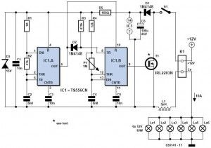

A dimmer is quite unusual in a caravan or on a boat. Here we describe how you can make one. So if you would like to be able to adjust the mood when you’re entertaining friends and acquaintances, then this circuit enables you to do so. Designing a dimmer for 12 V is tricky business.The dimmers you find in your home are designed to operate from an AC voltage and use this AC voltage as a fundamental characteristic for their operation. Because we now have to start with 12 V DC, we have to generate the AC voltage ourselves. We also have to keep in mind that we’re dealing with battery powered equipment and have to be frugal with energy.
The circuit that we finally arrived at can easily drive 6 lamps of 10 W each. Fewer are also possible, of course. In any case, the total current has to be smaller than 10 A. L1 and S1 can be adapted to suit a smaller current, if required. Note that the whole circuit will also work from 6 V. IC1 is a dual timer. You could also use the old faithful NE556, but it draws a little more current. IC1a is wired as an astable multivibrator with a frequency of 180 Hz. IC1b is configured as a monostable and is triggered, via D2, from the positive edge at the output of IC1a.
The length of the pulse that now appears at the output of IC1b is dependant on the position of P1. IC1b will be reset whenever the output of IC1a goes low, independent of the pulse duration, set with P1, R4 and C4. This guarantees that the dimming is smooth, even when the brightness is set to maximum.
12Volt dimmer circuit diagram
The output of IC1b (pin 9) drives the gate of MOSFET T1. When the duration of the pulses at the gate increases, the average time that the MOSFET is in conduction will also increase. In this way the brightness of the lamps is controlled. T1 conducts about 96 % of the time when the brightness is set to maximum. In this configuration, this can never be 100 %, because the 4 % of the time that the FET does not conduct is necessary to charge C6.
If the FET were to conduct with 100 % duty cycle, the power supply for the circuit would be effectively short-circuited. C6 allows the circuit to ride through the conduction period of the FET. D1 ensures that the charge cannot leak away via the FET during the ‘on’ period.
In the schematic, an IRL2203N is indicated for T1, but in principle you could use just about any power transistor (for example, BUK455, BUZ10, BUZ11 or BUZ100). The IRL2203 does however, have a very low ‘on’ resistance (RDS ON) of only 7 mΩ and can switch 12-V loads up to 5 A without a heatsink. If you choose a different MOSFET (with higher RDS ON) or use the circuit in a 6-V system then you will likely need a heatsink.
Using the IRL2203N with six lamps rated 12 V / 10 W, T1 dissipates only 170 mW. At 6 V and 10 A this becomes 680 mW. The circuit itself consumes about 0.35 mA at maximum brightness and about 1.25 mA at minimum.
12 Volt dimmer pcb layout
(View)
View full Circuit Diagram | Comments | Reading(3570)
Booster for Cable Radio
Published:2012/10/11 21:09:00 Author:muriel | Keyword: Booster, Cable Radio
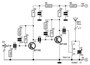
With the aid of this circuit it is possible to listen, using a portable VHF FM radio, to listen to stations that transmit only your local cable network. Both from its properties and its design this ‘cable booster’ appears similar to an antenna amplifier, because this is a two-stage amplifier with two common RF transistors type BF199.Only this time, the input is connected to the cable connection instead of an antenna while the output does not contain a coaxial connection but a tuned circuit that acts as impedance matching for a 1/4λ-antenna. If the circuit is tuned correctly (using trimmer C8), the amplified cable signal is radiated by the vertical antenna and can be easily received by a portable receiver up to three metres away.
Cable radio booster circuit diagram
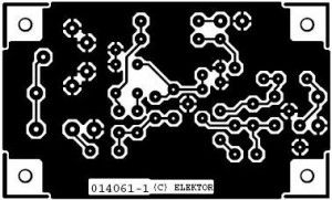
It is always possible to build the circuit on a piece of prototyping board, but because an RF-circuit is usually a little more critical it will probably work a lot better if you make use of the PCB layout shown here. During the design, the essential connections have been kept short and the ground plane has been made as large as possible. Capacitor C7 is best directly connected to the tap on L1, as can be seen in the photo. The (air-cored) coil consists of three turns of 1-mm enamelled copper wire (ECW) wound around a pencil (diameter about 8 mm).
Cable radio amplifier PCB layout
(View)
View full Circuit Diagram | Comments | Reading(1424)
Low voltage microphone preamplifier
Published:2012/10/11 21:09:00 Author:muriel | Keyword: Low voltage, microphone preamplifier
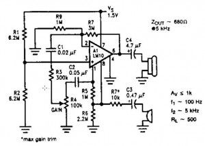
This is a low voltage microphone preamplifier circuit with a 1.5V power supply. The reference, with a 500 kHz unity-gain bandwidth, is used as a preamplifier with a gain of 100. Its output is fed through a gain-control potentiometer to the op amp, which is connected for a gain of 10. The combination gives a 60 dB gain with a 10 kHz bandwidth, unloaded, and 5 kHz loaded at 500 Ω . Input impedance is 10 kΩ.Potentially, using the reference as a preamplifier in this fashion can cause excess noise. However, because the reference voltage is low, the nose contribution, which adds root-mean-square, is likewise low. The input noise voltage in this connection is 440-500 nV Hz, about equal to that of the amp.
Microphone preamplifier circuit diagram
(View)
View full Circuit Diagram | Comments | Reading(1177)
Frequency Modulated Oscillator
Published:2012/10/11 21:09:00 Author:muriel | Keyword: Frequency, Modulated Oscillator
This FM oscillator can be used for wireless audio, microphone and part-15 applications where stable frequency modulated oscillators is needed. Lt can be varied to cover 75 to 150 MHz, as needed.
FM oscillator circuit schematic
(View)
View full Circuit Diagram | Comments | Reading(1832)
VLF VHF wideband active antenna
Published:2012/10/11 21:08:00 Author:muriel | Keyword: VLF, VHF, wideband, active antenna
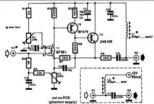
A 30 to 50 cm whip antenna provides reception from 10 MHz to over 220 MHz. T1 BF981, a dual-gate MOSFET, provides low noise, high-input impedance and high gain. The circuit is powered via the coaxial cable used to connect the antenna to a receiver.
Wideband active antenna amplifier circuit
(View)
View full Circuit Diagram | Comments | Reading(2460)
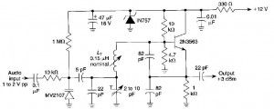
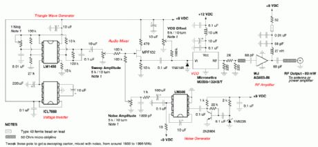
FM modulator circuit
Published:2012/10/11 21:08:00 Author:muriel | Keyword: FM modulator
The FM modulator circuit (frequency modulation) is built with a Motorola MC1648P oscillator. Two varactors, Motorola MV-209 are used to frequency modulate the oscillator. The 5000 Ω potentiometer is used to bias the varactors for the best linearity. The output frequency of approximately 100 MHz can be adjusted by changing the value of the inductor.
The output frequency can vary as much 10 MHz on each side. The output level of the modulator is -5 dBm. In this fm modulator prototype the varactor bias was 7.5V for the best linearity but this could be different with other varactors.
FM modulator circuit diagram
(View)
View full Circuit Diagram | Comments | Reading(3151)
70MHz RF power amplifier
Published:2012/10/11 21:08:00 Author:muriel | Keyword: 70MHz, RF, power amplifier
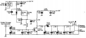
This 70MHz rf power amplifier circuit uses the SD1143 transistor which provides a gain of about 14dB in this design. It uses the fact that a 175MHz device has a much higher gain when used at lower frequencies. The amplifier was originally designed to be used with a transverter. The output is 8 to 10W for a 300 to 500 mW input power. Unfortunately, we dont have the coils values. With a few modifications you can use this amplifier for different frequencies.
70MHz power amplifier circuit diagram
(View)
View full Circuit Diagram | Comments | Reading(1461)
Beeper 110dB
Published:2012/10/11 2:36:00 Author:muriel | Keyword: Beeper, 110dB
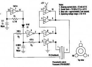
This beeper circuit will generate an car-splitting 110dB from 9V. The setup uses a single 74C14 (CD40106B) CMOS hex inverting Schmitt-trigger IC, which must be used with a piezoelectric device with a feedback terminal. The feedback terminal is attached to a central region on the piezoelectric wafer. When the beeper is driven at resonance, the feedback signal peaks.
One inverter of the 74C14 is wired as an astable oscillator. The frequency is chosen to be 5 times lower thant the 3,2KHz resonant frequency of the piezoelectric device. Feedback from the third pin of the beeper reinforces the correct drive frequency to ensure maximum sound output.
Four other inverter sections of the IC are wired to form two separate drivers. The output of one section is cross-wired to the input of the second section. The differential drive signal that results produces about 18Vpp when measured across the beeper. The last inverter section is wired as a second astable oscillator with a frequency of about 2 Hz. It gates the main oscillator on and off through a diode. For a continous tone, the modulation circuit can be deleted.
Beeper circuit diagram
(View)
View full Circuit Diagram | Comments | Reading(1284)
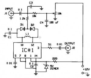
Stereo TV decoder
Published:2012/10/11 2:36:00 Author:muriel | Keyword: Stereo TV, decoder
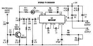
A simple stereo tv decoder circuit build with MC1310P. Transistor Q1 is an audio amplifier and U1 is used as a 31.5KHz subcarrier which is similar to 38KHz FM MPX. Pilot frequency is 15.734KHz.
Stereo tv decoder schematic
(View)
View full Circuit Diagram | Comments | Reading(4424)
27MHz NBFM Transmitter
Published:2012/10/11 2:36:00 Author:muriel | Keyword: 27MHz, NBFM Transmitter
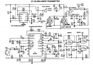
A 27MHz NBFM transmitter circuit schematic with MC2833 and 2 FET transistors MPF6660. Using a Motorola MC2833 one-chip FM transmitter, a few support components and am MPF6660 RF amp, this transmitter delivers up to 3W into a 50 Ω antenna. It is capable of operation over about 29 to 32 MHz with the components shown.
27MHz NBFM transmitter circuit diagram
(View)
View full Circuit Diagram | Comments | Reading(2858)
Stereo balance meter
Published:2012/10/11 2:35:00 Author:muriel | Keyword: Stereo balance, meter
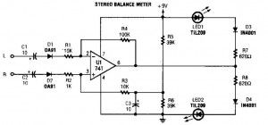
The simplest stereo balance meter circuit schematic available on the internet! When Left and Right signals are equal, no output is present from U1 and pin 6 is at a steady 4.5V. Unbalanced audio causes the LEDs to vary in brightness, which causes a difference that corresponds to unbalanced between channels.
Stereo balance meter circuit diagram
(View)
View full Circuit Diagram | Comments | Reading(0)
DC voltage regulator circuit
Published:2012/10/11 2:33:00 Author:muriel | Keyword: DC voltage, regulator
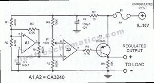
This circuit regulates a DC power output. It has a very wide application range. It can be used to control the speed of a motor, a pump, a toy train, the brightness of a LED or lamp, etc. Practically, it can be used in any application that uses a regulated DC power with pulse width modulation (PWM). It was originally used as a jumbo LED dimmer.The circuit works this way: the A1 opamp functions as a square wave generator. At its non-inverting input is a by product triangle wave signal. The IC A2 following it functions as a simple comparator. A reference voltage is fed to the inverting input of the A2 IC via the potentiometer P1. The output of A2 is a square wave signal with a constant frequency of around 200 Hertz. This signal has a variable pulse width from 0 to 100%.
DC regulator circuit diagram
(View)
View full Circuit Diagram | Comments | Reading(1524)
Musical doorbell circuit
Published:2012/10/11 2:33:00 Author:muriel | Keyword: Musical doorbell
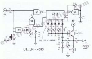
In many cases, a doorbell that sounds off a musical tone is preferable over the common buzz sound. This featured circuit is a musical doorbell. After the button S1 is pressed, a short melody is played. When the button is pressed many times in rapid succession or pressed longer, a different melody is generated and the melody plays longer.The circuit works this way: when the button S1 is activated the inputs of U3 and one input of U1 switches to logic “0″. The data input (pin 7 of IC 4015) becomes logic “1″. The 4015 is a static 4-bit shift register. Each clock impulse coming from U4 shifts this logic “1″ further in the register. The clock frequency is around 5 Hz.
The number of shifted logic “1″ is directly dependent on the length of time the switch S1 is closed. Once at least one shift register is logic “1″, a current flows to the base of T1 through a corresponding resistor. The transistor T1 functions as a current controlled oscillator. The tone pitch is dependent on the logic state of the different flip-flop outputs of the shift register. Each clock pulse shifts the logic “1″ in the register. One output of the register (pin 2) is coupled back to U2 and U3 so that all the logic “1″ in the register always run in a loop.
Musical doorbell circuit diagram
When S1 is released (opened), the register runs until the capacitor C1 gets discharged through R2. When S1 is again pressed (closed), the capacitor C1 stays charged causing the musical bell to play continously.
The difference between two ways of activating the switch S1 is that different combinations of logic “1″ are inputted into the shift register. These different combinations produce the different melodies plyed by the circuit. The musical doorbell must be connected to an audio amplifier. The supply voltage is not critical. It can be between 5 and 15 volts. The circuit consumes around 15mA.
(View)
View full Circuit Diagram | Comments | Reading(1945)
Simple siren circuit
Published:2012/10/11 2:32:00 Author:muriel | Keyword: Simple siren circuit
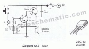
This circuit generates a tone that sounds very similar to a siren. The generator part of the circuit is made of the combination of PNP and NPN transistors. Toghether, the two transistors build up a free runing multivibrator. If the C2 capacitor was connected to the positive line of the power supply, it would have worked as a constant frequency oscillator.However, we dont want a constant frequency oscillator. We want a siren. So to generate an up and down going signal tone, the resistor R2 is fed from an RC circuit. When the switch S1 is pressed, the capacitor C1 charges via R1 slowly until it reaches the maximum voltage level of 4 volts. This increasing voltage results to a decreasing time constant at the R2/C2 junction. This furthermore results to an increasing frequency of the multivibrator.
After the switch S1 is released, the capacitor C1 discharges slowly resulting to a decreasing frequency cycle. Through the combination of the two time constants a sawtooth waveform is generated.The signal heared from the speaker will be an increasing or decreasing tone depending on whether the switch S1 is pressed or released.
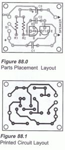
Siren circuit diagram
Siren PCB layout
(View)
View full Circuit Diagram | Comments | Reading(2104)
Signal meter circuit
Published:2012/10/11 2:32:00 Author:muriel | Keyword: Signal meter
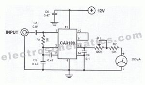
The CA3189 IC integrates a symmetrical limiter, a phase demodulator, an audio amplifier, and a logarithmic detector-amplifier. The logarithmic detector-amplifier is the most interesting part of the IC for the above featured circuit. It can be used to enhance the “logarithmic signal meter” of shortwave receivers to make the signal reading more accurate.Building the circuit is very simple. It must be built in such a way that it will work up to 30 MHz. To do that, follow these guidelines: connect the input to a 50 Ω line; make the circuit wiring as short as possible; and the input signal must be shielded.
Signal meter circuit schematic
(View)
View full Circuit Diagram | Comments | Reading(1422)
Crystal tester
Published:2012/10/11 2:32:00 Author:muriel | Keyword: Crystal tester
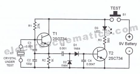
The idea for this crystal tester circuit sprung out of the need of testing a large number of oscillator crystals lying unused in a big hobby box. testing the crystals one by one without the appropriate device would have been very slow and a time consuming task. Commercial crystal testers are however very expensive, that is why this simple electronic crystal tester was born.The transistor T1 and the crystal to be tested together makes a complete crystal oscillator. The capacitors C1 and C2 works as a capacitive voltage divider that is connected to the transistor T1. If the crystal being tested is intact, the circuit oscillates. The sine wave oscillation voltage is fed to the rectifier circuit (d1, D2) and filtered by capacitor C4. With an intact crystal, the DC voltage at the base of the transistor T2 is high enough to cause the transistor to conduct. The LED lights up signalling that the crystal is good.The electronic circuit cand be used to test crystals with frequencies from 100kHz up to 30MHz. The current consumption is low: around 25mA.
Crystal Tester Circuit Diagram
(View)
View full Circuit Diagram | Comments | Reading(0)
Loudspeaker peak indicator
Published:2012/10/11 2:32:00 Author:muriel | Keyword: Loudspeaker, peak indicator
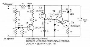
Modern loudspeakers boxes are relatively insensitive to overdriving signals, however it is still important to limit the power driving it to avoid clipping of the audio signal. A broken sound from an overdriven loudspeaker is not only annoying to the the ears but also the loudspeaker itself can be damaged by the continous uncontrolled signal peaks.
This peak indicator circuit is very useful aid in detecting the driving limits of a loudspeaker system. It can e directly connected to the existing speaker wirings and needs no extra power. It can detect very short voltage overswings and therefore provides reliable means of determing the driving limits of a loudspeaker.
The threshold of the peak indicator can be set for speakers ranging from around 15 watts to 125 watts with 8 ohms impedance. For 4 ohms speakers, the indicator can be set for 30 watts up to 250 watts. By testing speakers, occasional blinking of the LED does not mean danger but when the LED blinks very often then it is advisable to reduce the volume of the amplifier.
Loudspeaker peak indicator circuit diagram
The circuit operates this way: During operation the signal charges C2 through R1 and D1. In standby periods, all transistors are turned off and no current flows through the LED. A sample of the signal flows through P1 and enters T1. P1 controls the threshold level of T1. Once the signal sample exceeds the threshold lvel, T1 and T2 switch on and charges C1 as a result; T1 conducts amd switches T4 on.
When signal goes down, T1 and T2 turn off but since C1 discharges slowly T3 and T4 remain conducting for about one second longer causing the LED to also light up longer. This tehnique has the advantage of indicating short time signal overswings which are normally not detectable.
In constructing this peak indicator circuit it is advisable to use high luminance LEDs with a diameter of not less than 3mm.
Peak indicator PCB and parts
(View)
View full Circuit Diagram | Comments | Reading(2059)
9V battery indicator circuit
Published:2012/10/11 2:30:00 Author:muriel | Keyword: 9V, battery indicator
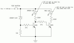
This is a very simple 9V low battery indicator circuit which has 2 LEDs, one green which will light up when the battery voltage is higher than 6.9 volts and one red LED which will light up when the battery voltage is bellow 6.9 volts. You can use BC547 … BC549 .
Low battery indicator circuit diagram
(View)
View full Circuit Diagram | Comments | Reading(2642)
Cell phone jammer circuit
Published:2012/10/11 2:30:00 Author:muriel | Keyword: Cell phone, jammer
A beautiful diy gsm jammer or mobile cell phone jammer schematic diagram for use only in GSM1900 with frequency from 1930 MHz to 1990 MHz. The GSM1900 mobile phone network is used by USA, Canada and most of the countries in South America.
Mobile cellphone jammer circuit diagram
This cell phone jammer is not applicable for use in Europe, Middle East, nor Asia.The GSM jammer circuit could block mobile phone signals which works on GSM1900 band, also called DCS. For more cell phone jammers check the related posts.
(View)
View full Circuit Diagram | Comments | Reading(2498)
| Pages:306/2234 At 20301302303304305306307308309310311312313314315316317318319320Under 20 |
Circuit Categories
power supply circuit
Amplifier Circuit
Basic Circuit
LED and Light Circuit
Sensor Circuit
Signal Processing
Electrical Equipment Circuit
Control Circuit
Remote Control Circuit
A/D-D/A Converter Circuit
Audio Circuit
Measuring and Test Circuit
Communication Circuit
Computer-Related Circuit
555 Circuit
Automotive Circuit
Repairing Circuit