
Circuit Diagram
Index 311
White LED Flood Lamp circuit
Published:2012/10/9 2:30:00 Author:muriel | Keyword: White LED, Flood Lamp
This White LED lights illuminates your porch with cool white light. The circuit is too simple and energy saving design. Its current consumption is practically nil but can provide light like a 20 watt CFL lamp. It is directly connected to AC lines to eliminate a bulk transformerUltra White LED Lamps are now replacing the fluorescent lamps due to its energy saving property and simplicity of design. White LED emits 1000 to 6000 MCD light and easily works on 3 volts at 20 mA. White LEDs are available as spot light and diffuse type versions. Different sizes like 3mm, 5mm and 10 mm varieties are now common. High watt single white LED is also available. White LEDs was introduced in 1990 which uses Indium Gallium Nitride (InGaN) as the semiconductor. White LED contains a blue chip with white inorganic Phosphor.
When blue light strikes the phosphor, it emits white light. The circuit uses capacitive reactance to drop high volt AC to low volt AC. This reduces power loss due to heat dissipation. The value of the AC capacitor can be calculated using the formula X c= 1/ (2 π f C) where, Xc is the reactance in ohms, C the capacitance in farads and f the mains frequency. Xc = Vrms / I where Vrms is the input voltage and I is the current flowing through LEDs. The low volt AC (around 100 volts) dropped by C1 is then rectified by a full wave rectifier formed of D1-D4.
Capacitor C2 act as a ripple remover and buffer. Zener diode ZD regulates DC to 69 volts and prevents excess reverse voltage across the LEDs during the negative half cycles.R1 is a must in the circuit to bleed the stored current from C1 when the circuit in unplugged. C1 can store more than 400 volts for many days if R1 is not connected. This can give a lethal shock.
R2 reduces the inrush current.20 LEDs are connected as a string to obtain luminance equal to 20W CFL. Enclose the circuit in a shock proof case. If a reflector is provided behind the LEDs, it will give a flood light appearance.
Important! Do not touch any points or trouble shoot when the circuit is connected to mains.
Caution This is an AC powered circuit and can give fatal shock if handled carelessly. Do not construct the circuit unless you are competent to handle high volt circuits.
LED Lights Circuit Diagram
(View)
View full Circuit Diagram | Comments | Reading(1765)
Digital Volume Control Circuit
Published:2012/10/9 2:30:00 Author:muriel | Keyword: Digital, Volume Control
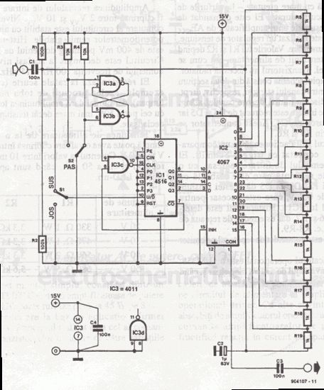
The heart of this digital volume controller DVC circuit is IC2 4067, 16-channel analog multiplexer.Because the 1kΩ has been connected between every input and output, the multiplexer can act like a potentiometer. The total resistance is 15kΩ . You can use different values for the resistor to obtain a different characteristic. The current consumption is 1mA.
Digital Volume Control Circuit Diagram
(View)
View full Circuit Diagram | Comments | Reading(2959)
Temperature indicator circuit
Published:2012/10/9 2:30:00 Author:muriel | Keyword: Temperature indicator
The multimeter is a measurement device most used by engineers and we use it in this temperature indicator circuit schematic. The temperature sensor is LM335 wich has a linear characteristic of 10mV / K . In the production process this electronic device is calibrated so can provide 2.73V at 00C.LM336 is used as a very precise 2.5V Zener diode; CA3040 amplification can be adjust between 1.08 and 1.10 times thru P1. This temperature measurement circuit can be used for Fahrenheit measurements, in this case the freezing point is adjusted at 320F. At 2120F, P2 is adjusted to obtain 0.9V at output.So 10F correspond to 5mV. The total current consumption is 10mA.
Temperature sensor circuit diagram
(View)
View full Circuit Diagram | Comments | Reading(824)
Solar based Multipurpose Charger circuit
Published:2012/10/9 2:30:00 Author:muriel | Keyword: Solar,Multipurpose Charger
Here is an ideal solution to harvest Solar energy for charging purpose. This charger can replenish almost all types of batteries including Mobile phone battery. It uses a Solar Module to convert light energy into electrical energy
Solar Charger Circuit Schematic
The circuit is self explanatory. A 12 volt 5 Watt solar panel is used as the source of current. The cells in the panel are made up of semiconductor material which transforms light energy into electrical energy. When the sunlight is maximum, the solar module can generate around 16.5 volts at 400 mA. This current is used to charge the battery. Diode D1 allows current into three regulator ICs to provide regulated voltage to the load. IC1 7812 gives 12 volts and 400 mA current to charge a Lead Acid battery.
The battery can be connected to point C and ground. IC2 7806 gives regulated 6 volts to charge NiCd battery. Resistor R3 restricts the charging current. IC3 7805 provides regulated 5 volts to charge all types of Mobile phone batteries which are rated at 3.6 volts. Resistor R2 restricts charging current to a safer level. Point A can also used to charge Lithium ion and NiMh batteries. High value capacitors C1 and C2 act as current buffers so that a short duration interruption in current flow from the panel will not affect the charging process. Red LED indicates the charging process. (View)
View full Circuit Diagram | Comments | Reading(1564)
UM3561 Siren Generator Design
Published:2012/10/9 2:29:00 Author:muriel | Keyword: UM3561,Siren Generator
UM3561 is an excellent ROM IC that can generate Multi siren tones simulating Police siren, Ambulance siren, Fire brigade siren and Machine gun sound. This 8 pin low power IC can work down to 2.4 volts.
The UM 3561 is a low cost siren generator designed for use in toy applications. The IC has an inbuilt oscillator and tone selection pins. It is easy to make a siren generator with only a few external components. Only one external resistor and a speaker driver transistor are sufficient to make a simple siren generator.Inside the UM3561Inside the IC, there is an oscillator circuit and the frequency of oscillations is controlled by the external resistor connected to OSC 1(Pin 7) and OSC2 (Pin 8). A 220 K resistor will give satisfactory results. The oscillations thus generated will be then transferred to a control circuit which function based on the tone selection through the connections of SEL 1 (Pin 6) and SEL2 (Pin 1) . The control circuit passes the signal to an address counter and then to the ROM. The tone pulses thus generated will be available from the output pin 3. Since the sound is weak, an amplifier is necessary to get loud sound. A single NPN transistor will amplify the sound.
Pin Assignment
Pin 1 Tone Sel.2Pin 2 GndPin 3 OutputPin 4 NC- Used for testing purposePin 5 +3VPin 6 Tone Sel .1Pin 7 Osc 1Pin 8 Osc 2
Tone Selection
By changing the pin connections of Sel.1 (Pin6) and Sel. 2(Pin 1) it is easy to change the siren tones.Sel 1Sel 2TonePin 6 Pin 1NC NC Police siren+3V NC Fire Engine soundGnd NC Ambulance SirenNC +3V Machine Gun sound
UM3651 Siren Generator Circuit Diagram
(View)
View full Circuit Diagram | Comments | Reading(1128)
Delay On Circuit
Published:2012/10/9 2:29:00 Author:muriel | Keyword: Delay On Circuit
Protect your LCD or Plasma TV with this tiny delay on circuit. The SMPS based power supply of these modern electronic devices is vulnerable to spikes in the mains line so it gives a time delay of one minute before applying power to the device. This prevents deleterious effects due to inrush current and spurious spikes at power on.Inrush current at power on or power resumes after a power failure can cause unexpected damage in SMPS based power supply of electronic devices. The spurious spike in the power supply when power resumes is due to heavy magnetic flux in the distribution transformer in the mains network. If a short delay is provided, such damages can be avoided. The circuit descried here is intended for this purpose. It gives power to the device only after one to two minutes of delay after the power is switched on. The circuit is a zener controlled switch.
Capacitor C1 charges through R1 and VR. When the voltage in C1 rises above 3.1 volts, zener conducts to trigger T1. The relay connected to the collector of T1 energizes and power will be available through the common and Normally Open contacts of the relay. Relay remains latched as long as the voltage level in the mains is normal. Capacitor C2 keeps the base bias of T1 steady so that relay clicking can be avoided. Diode D1 prevents back e.m.f when T1 switches off. Red LED indicates the Relay On status. Delay time depends on the value of C1.
Delay-On Circuit Diagram
Power to the circuit can be derived from a standard 12 volt transformer with rectifier and smoothing capacitor. Use a socket to connect the TV as shown.
(View)
View full Circuit Diagram | Comments | Reading(851)
Reflex Tester Circuit
Published:2012/10/9 2:28:00 Author:muriel | Keyword: Reflex Tester
Testing human reaction speed is not only a fun way of spending time, but also allows the drawing of conclusions, for example on the skills of a momentary driver. When the contact closes the power button, the astabil multivibrator built with IC1 produces pulses that are applied to counter IC3. D1 …. D10 LEDs light up sequentially in a chained fast.Once the person tested acts stop button S2 the astabil multivibrator is blocked, the last ordered with decoder IC4 LED lights next. If frequency of the astabil multivibrator with P1 is adjusted so that the numerator, for example, receives a pulse every 10 seconds, then the reaction time can be read easily. The test can be repeated after drive reset button (S3). Reflex tester circuit absorbs about 120 mA current, supply voltage (5V) must be stabilized. Frequency can be adjusted to the astabil multivibrator with P1 between 10 Hz and 80 Hz.
Reflex Test Circuit Diagram
(View)
View full Circuit Diagram | Comments | Reading(1363)
Battery Monitor Circuit
Published:2012/10/9 2:28:00 Author:muriel | Keyword: Battery, Monitor
Here is a simple Battery Monitor circuit for a quick check of 12 volt Lead-Acid Battery. Battery charge should be constantly monitored to increase the life of the battery. Overcharge as well as under charge will reduce the battery life. The terminal voltage of the Lead Acid battery should be with in the range of 12.5 to 13.5 volts. If the battery voltage reduces below 10 volts for long period, battery will not accept any charging current. Similarly if the terminal voltage exceeds above 14 volts, battery will be destroyed.The circuit is a Zener controlled transistor switch lighting three LEDs Red, Green and Yellow to show battery states like Low, Normal and High. When the battery voltage is less than 11 volts, Zener diodes ZD1 and ZD2 cease to conduct and Red LED only lights indicating low battery condition. If the voltage is between 12 volt and 14 volts, Zener diode ZD1 forward bias and T1 conducts. The Green LED connected to the collector of T1 lights indicating normal voltage. If the battery voltage exceeds 15 volts, Zener diode ZD2 also conducts and T2 forward bias. This lights Yellow LED indicating over charge. Thus the following indications can be obtained
Red Low voltageGreen Normal voltageGreen and Yellow Over voltage
Battery Monitor Circuit Diagram
(View)
View full Circuit Diagram | Comments | Reading(716)
Points, line overflow LED display circuit with LM3914
Published:2012/10/8 21:01:00 Author:Ecco | Keyword: Points, line overflow, LED display
This circuit is in point working mode when it has no overflowing. When it is overflowing, LED changes into line display mode, thus indicating the overflowing.
(View)
View full Circuit Diagram | Comments | Reading(4914)
Basic structure of LED light column display
Published:2012/10/8 21:12:00 Author:Ecco | Keyword: Basic structure , LED, light column , display
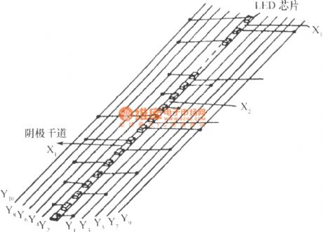
In this structure, high brightness light emitting diode chips are arranged in a straight line, and 100 chips are divided into 10 groups, each group has 10 chips. Each group shares a common cathode, and every anode with the same medium sequence is attached to the anode roads Y1,Y2,...,Y10, 10 cathodes are respectively X1,X2,...,X10, then they constitute a 10x10 matrix. This device works with matrix-scanning mode, so it is called matrix-scanning beam display device. This device also set a chip under zero line of in device settings for indicator.
(View)
View full Circuit Diagram | Comments | Reading(1140)
The dynamic driving interface circuit between SAA1064 serial I2C bus and LED display IC
Published:2012/10/8 22:06:00 Author:Ecco | Keyword: dynamic driving, interface circuit, serial I2C bus , LED display IC
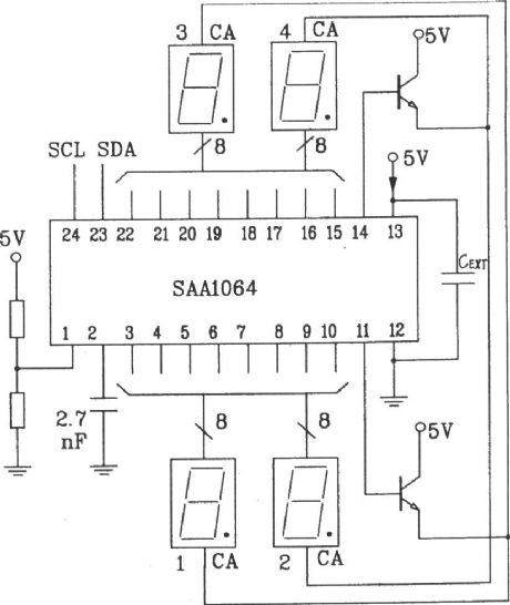
Due to the SAA1064's dynamic scanning display depends on the the multiplexer swicthing data latch and time control circuit, the master does not have to intervene, and the dynamic work can best play SAA1064 function, so it is the most common working way. LED -bit numbers in figure and selected data sequence in data manipulation format are corresponding. CEXT is the clock oscillation capacitor which guarantees to work signal for dynamic driving. MX1, MX2 are the common electrode driving signal output terminals of monitor. When it is dynamic scanning, MX1 , MX2 's timing waveforms are shown in Figure as below.
(View)
View full Circuit Diagram | Comments | Reading(2017)
Christmas lights circuit with optocoupler
Published:2012/10/8 22:25:00 Author:Ecco | Keyword: Christmas lights , optocoupler
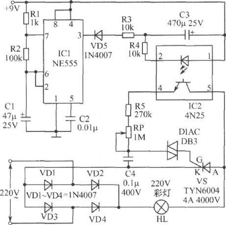
When the power is turned on, the lantern HL is brighter gradually; when it is brightest, it will be darken automatically; if it is darkest, it will be automatically gradually brighter. The whole process is smooth. Lantern HL's luminance change depends on the charging and discharging of the capacitor C3. When the pin 3 of IC1 (NE555) outputs high, capacitor C3 begins to discharge, and the brightness of the lantern HL begins to decline by IC2 (CN25) optical isolation. IC1 here is set astable oscillator, of which frequency is determined by R1, R2 and C1.
(View)
View full Circuit Diagram | Comments | Reading(2234)
The application circuit of dual-axis magnetic field sensor (integrated magnetic sensor HMC1002) with S / R circuit and serial interface
Published:2012/10/8 22:50:00 Author:Ecco | Keyword: application circuit, dual-axis, magnetic field , sensor , integrated magnetic sensor, S / R circuit , serial interface
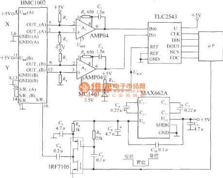
It can use a dual - axis magnetic field sensor HMC1002 and two AMP04 draws ( A1, A2 ) to simultaneously measure the magnetic field with X - axis direction and the Y-axis direction. The HMC1002 outputs two ways of voltage signals which are respectively amplified by A1 and A2, then they are input to the analog input terminal and reference terminal 12 of A / D converter TLC2543 and connected to interface circuit μP. The MAX662A is high-efficiency DC / DC converter which can raise +5 V power supply to +10 V to drive IRF7105. The driver's input signal is from μP, and it outputs pulse current to S / R + terminal ( pin 16 ) of HMC1002. C3 shown in figure should be used tantalum capacitor.
(View)
View full Circuit Diagram | Comments | Reading(1508)
1 Hz Pulse Frequency Generator
Published:2012/10/8 2:51:00 Author:muriel | Keyword: 1 Hz, Pulse Frequency Generator
Here is a 1Hz pulse/frequency generator using the popular timer IC 555 which is wired as an Astable Multivibrator. The output pulses can be indicated visually by the LED. An Astable Multivibrator, often called a free-running Multivibrator, is a rectangular-wave generating circuit. Unlike the Monostable Multivibrator, this circuit does not require any external trigger to change the state of the output, hence the name free-running. This circuit can be used in applications that require clock pulses
1Hz Pulse Generator Circuit Diagram
An Astable Multivibrator can be produced by adding resistors and a capacitor to the basic timer IC 555.The timing during which the output is either high or low is determined by the externally connected two resistors and a capacitor.Clock: A clock is simply a square wave i.e. alternate high & low states. Each alternate high-low forms a clock cycle with a specific frequency & duty cycle. Frequency is the number of cycles completed in 1 sec & duty cycle is the ratio of the time period of high state to the time period of the low state
We can set the 555 to work at the desired frequency by selecting the right combination of resistances & capacitance.
Frequency = 1.44 / {(R1 + 2R2) * C1}
Also, 555 can produce waves with duty cycle else than the 50 % cycle.
Duty Cycle = (R1 + R2) * 100/ (R1 + 2R2)where duty cycle= Ratio of time period when the output is 1 to the time period when the output is 0
(View)
View full Circuit Diagram | Comments | Reading(1491)
Pachisi Game Circuit
Published:2012/10/8 2:50:00 Author:muriel | Keyword: Pachisi Game
Pachisi game is designed for two persons. Each player has one figurine; the figurines are found in the early game on positions indicated by arrows. The goal of each figurine is the white square field in the middle of the game. Players move in turn: they need to move the figurines forward or back on the next black or white field. If a player reaches with his figurine on a field that already is occupied by the other player then he wins.4 LEDs indicate if the figure should be moved forward or back, or should be put on the next field white or black. By pressing S1, LEDs indicate by chance, randomly “before” or “back” and “black” or “white”.
The assembly is not complicated: two bistable multivibrators form a binar counter with 2 bits. Leds are used to make visible the counter position; the 4 transistor are sued to power up the LEDs.
Pachisi Game Circuit Diagram
Pachisi Game Table Board
(View)
View full Circuit Diagram | Comments | Reading(938)
Mock Flasher LED circuit
Published:2012/10/8 2:50:00 Author:muriel | Keyword: Mock Flasher, LED
This simple Mock Flasher LED simulates the indicator of a sophisticated Alarm system. It can be placed in doors, gates and vehicles to confuse intruders. The circuit is too simple using a Unijunction transistor as an oscillator.Uni junction transistor (UJT) is an electronic semiconductor device that has only one junction. The UJT has three terminals: an emitter (E) and two bases (B1 and B2). The base is formed by lightly doped n-type bar of silicon. Two ohmic contacts B1 and B2 are attached at its ends. The emitter is of p-type and it is heavily doped. The resistance between B1 and B2, when the emitter is open-circuit is called inter-base resistance. The 2N2646 is the most commonly used version of the UJT.
UJT 2N2646
UJT Pin Connection -Bottom View
Working of UJT
The UJT is biased with a positive voltage between the two bases. This causes a potential drop along the length of the device. When the emitter voltage is driven approximately one diode voltage above the voltage at the point where the P diffusion (emitter) is, current will begin to flow from the emitter into the base region. Because the base region is very lightly doped, the additional current (actually charges in the base region) causes conductivity modulation which reduces the resistance of the portion of the base between the emitter junction and the B2 terminal. This reduction in resistance means that the emitter junction is more forward biased, and so even more current is injected. Overall, the effect is a negative resistance at the emitter terminal. This is what makes the UJT useful, especially in simple oscillator circuits.
Working of Mock Flasher LED
UJT 2N 2646 is used as a simple oscillator with the oscillating components R1 and C2. The LED is connected between the base2 (B2) of the UJT and the ground. Resistor R2 restricts current through the UJT as well as LED. At power on, capacitor C2 charges through R1 and when it fully charges, emitter of UJT forward biases and current flows into the base. LED then lights. The discharge of C2 is followed by its charging again creating an oscillating cycle so that LED flashes.
Mock Flasher LED Circuit Diagram
(View)
View full Circuit Diagram | Comments | Reading(1308)
Light Sensitive Switch Circuit
Published:2012/10/8 2:49:00 Author:muriel | Keyword: Light Sensitive, Switch
There are a wide range of applications for light sensitive switches: lighting, entrance door, automatic staircase, automatic opening of doors to the action of a ray of light, alarm systems, etc… Many of us are familiar with photosensitive switches made with a single transistor that is controlled by a photoresistor placed between the base and the recharger, depending on what is desired: normal functioning “closed” or normal “open” the switch.This configuration allows easy installation more complex, involving the use of operational amplifiers, especially those of type 741, which are very cheap. Another way to optodetect, less known, uses a bridge assembly, which operates on the principle that when the current is zero diagonal axle, means that the bridge is balanced.
This last principle is used in the sensitive switch installation you will be presented next. Photocell is placed in a bridge circuit and a comparator is used as detector bridge balanced. The comparator’s output control thyristor through a transistor. In this circuit, protective measures must be taken because it is isolated from the network.
Light Switch Circuit Diagram
Power supply circuit is taken from the bridge rectifier D1…D4 is filtered and stabilized by R1, C1, and D5. The bridge circuit is difficult to identify in the given diagram, but it is made of R2 ….. R4, P1 and photoresist (LDR). IC1 is used in the comparator configuration and power level will be about 1.8 V when potential entry vice versa (negative) exceed that of the entry non vice versa. Resistance R5 conducts a hysteresis of about 1V to prevent thyristor to oscillate at T1 and threshold lighting.
Switching point of the light sensitive switch may be adjusted from P1. With the potentiometer set the minimum (minimal resistance) lamp will light a crepuscular light. If you want more flexibility, replace P1 with one that has a value of 1 MΩ. If desired operation reverse position in the scheme of the photoresistor can be changed with the group P1/R4. LA1 lamp will be extinguished, in this case, after dark.
Some practical advice: if you want to use higher power lamps then diodes D1 …. D4 need to be replaced with other type 1N5404 and thyristor TH1 will be equipped with a heat sink. With these changes, the circuit can control currents up to 3A.
Maximum gate for TH1 is 250 µA, which means that you must use a very sensitive thyristor. It can use any type of photoresistor. Remember precautions to be taken due to lack of isolation mounting over the network. It is important that the entire circuit to be protected in a plastic box, of any shape, provided with a hole in the upper side, in order to allow to the photoresistance “to see”. Assure that the entry cable and the exit cable are fixed. This precautions will assure you from accidents.
Light Sensitive Switch PCB Layout
(View)
View full Circuit Diagram | Comments | Reading(1269)
LASER Door Alarm circuit
Published:2012/10/8 2:49:00 Author:muriel | Keyword: LASER, Door, Alarm
This laser door alarm is based on the interruption of Laser beam. A low cost Laser pointer is used as the source of light beam. When somebody breaks the laser path, the alarm will be generated for few seconds.
Laser Door Alarm Circuit Diagram
The laser door alarm circuit has two sections. The laser transmitter is a laser pointer readily available. It should be powered with 3 volt DC supply and fixed on one side of the door frame. The receiver has a Phototransistor at the front end. L14F1 NPN Darlington phototransistor is used as the laser sensor. IC1 is used as a voltage comparator with its inverting input tied to a potential divider R2-R3. So that the inverting input is kept at half supply voltage.
The non inverting input receives a variable voltage based on the conduction of T1. The receiver should be fixed on the opposite door frame and should be properly aligned to the laser beam. Normally the laser beam illuminates the face of phototransistor and it conducts. This keeps the voltage at pin 3 lower than pin 2 of IC1.
As a result, output of comparator remains low. LED and Buzzer remain off in this state. When a person crosses the door, laser beam breaks and T1 cease to conduct. Collector voltage of T1 rises and voltage at pin 3 of comparator increases and its output becomes high. This activates LED and buzzer. Capacitor C1 keeps the base of T2 high for few seconds even after the output of IC1 becomes low again. C2 gives current to the buzzer for few seconds even after T2 turns off.
Caution: This circuit uses harmful laser rays. Do not look into the Laser pointer. It should not be placed in places accessible to children.
(View)
View full Circuit Diagram | Comments | Reading(1419)
PC Fan Controller circuit
Published:2012/10/8 2:48:00 Author:muriel | Keyword: PC Fan, Controller
This PC fan controller circuit is designed with discrete components and is used to control 12 V fans that have a current consumption lower than 200 mA. With the components values presented in the circuit diagram, the voltage won’t drop below 7 V. If the fan won’t start at 250C then temporarily replace the temperature sensor KTY10 with a 1.8 kΩ resistor and reduce the value of R7. If the PC fan has a speed too high then increase the R7 value.T1 and T2 transistors compare the fixed potentional from R3-R4 common point with the temperature dependent potentional of R1-R2 common point. It may be useful to connect a 25 kΩ potentiometer instead of R2 and to adjust it until the PC fan is at the correct speed and to measure its resistance and then replace it with a fix resistor with the same value.
PC Fan Controller Circuit Diagram
Place the temperature sensor in the warm air of the fan. When the PC is connected the speed rotation of the fan will be pretty high because of C1 but will decrease at a minimum value. Measure with a thermometer the air temperature close to the sensor. When the temperature reaches 350C the pc fan controller circuit will start to work. If this won’t happen modify the value of R2 or adjust a potentiometer placed instead of R2. When the temperature increases so will the rotation speed of the PC fan. The maximum speed will be lower than the one obtained without the control circuit. (View)
View full Circuit Diagram | Comments | Reading(1293)
Temperature to Voltage Converter circuit
Published:2012/10/8 2:47:00 Author:muriel | Keyword: Temperature to Voltage, Converter
With this simple temperature to voltage converter circuit we can do a precise measurement of the temperature in a room. A NTC resistor or a thermistor is used as a sensor that has a strong temperature dependence.If the NTC temperature rises then the output voltage rises with 0.5 V per 10C.Conversion factor depends on the type of thermistor resistance used. If you want to read the temperature directly on an universal measurement device then the value of R9 must be choosed so that the desired sensitivity is achieved (R8 must be equal with R9).The power supply voltage level is not critical; D1 zener voltage can be between 4.7 V and 8.2 V. The current consumption is about 12 mA.
Temperature-Voltage Converter Circuit Diagram
(View)
View full Circuit Diagram | Comments | Reading(1271)
| Pages:311/2234 At 20301302303304305306307308309310311312313314315316317318319320Under 20 |
Circuit Categories
power supply circuit
Amplifier Circuit
Basic Circuit
LED and Light Circuit
Sensor Circuit
Signal Processing
Electrical Equipment Circuit
Control Circuit
Remote Control Circuit
A/D-D/A Converter Circuit
Audio Circuit
Measuring and Test Circuit
Communication Circuit
Computer-Related Circuit
555 Circuit
Automotive Circuit
Repairing Circuit