
Circuit Diagram
Index 305
Improved 3 Transistor Audio Amp (80 milliwatt)
Published:2012/10/11 21:32:00 Author:muriel | Keyword: Improved, 3 Transistor, Audio Amp, 80 milliwatt
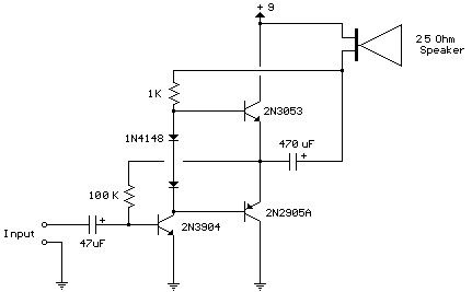
This circuit is similar to the one above but uses positive feedback to get a little more amplitude to the speaker. I copied it from a small 5 transistor radio that uses a 25 ohm speaker. In the circuit above, the load resistor for the driver transistor is tied directly to the + supply. This has a disadvantage in that as the output moves positive, the drop across the 470 ohm resistor decreases which reduces the base current to the top NPN transistor. Thus the output cannot move all the way to the + supply because there wouldn't be any voltage across the 470 resistor and no base current to the NPN transistor.
This circuit corrects the problem somewhat and allows a larger voltage swing and probably more output power, but I don't know how much without doing a lot of testing. The output still won't move more than a couple volts using small transistors since the peak current won't be more than 100mA or so into a 25 ohm load. But it's an improvement over the other circuit above.
In this circuit, the 1K load resistor is tied to the speaker so that as the output moves negative, the voltage on the 1K resistor is reduced, which aids in turning off the top NPN transistor. When the output moves positive, the charge on the 470uF capacitor aids in turning on the top NPN transistor.
(View)
View full Circuit Diagram | Comments | Reading(1080)
3 Transistor Audio Amp (50 milliwatt)
Published:2012/10/11 21:31:00 Author:muriel | Keyword: 3 Transistor, Audio Amp, 50 milliwatt
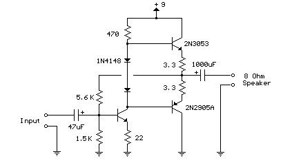
Here is a little audio amplifier similar to what you might find in a small transistor radio. The input stage is biased so that the supply voltage is divided equally across the two complimentary output transistors which are slightly biased in conduction by the diodes between the bases. A 3.3 ohm resistor is used in series with the emitters of the output transistors to stabilize the bias current so it doesn't change much with temperature or with different transistors and diodes. As the bias current increases, the voltage between the emitter and base decreases, thus reducing the conduction. Input impedance is about 500 ohms and voltage gain is about 5 with an 8 ohm speaker attached. The voltage swing on the speaker is about 2 volts without distorting and power output is in the 50 milliwatt range. A higher supply voltage and the addition of heat sinks to the output transistors would provide more power. Circuit draws about 30 milliamps from a 9 volt supply.
(View)
View full Circuit Diagram | Comments | Reading(1706)
Bad Light Bulb Indicator
Published:2012/10/11 21:27:00 Author:muriel | Keyword: Bad Light, Bulb Indicator

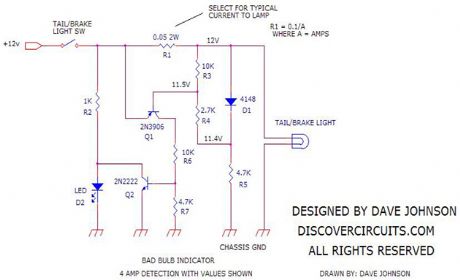


This request came from a Discover Circuits visitor. He wanted to turn on a LED indicator light whenever a circuit detected a burned out tail/brake light on a car or truck. The circuit shown below uses a transistor switch, to detect current flowing through a low value resistor. If current is flowing to a light bulb, the circuit shunts current around a LED light, keeping the LED turned off. If there is no current detected, the LED turns on. The circuit should operate from 6v to 24v.
The shunt resistor needs to be selected, so the current flowing to one light bulb generates at least 0.1 volts across the resistor. Since most turn signals illuminate two light bulbs at one time, this circuit may not detect a single burned out bulb, until the tail lights are turned on or until the car brakes are applied.
(View)
View full Circuit Diagram | Comments | Reading(2624)
TDA 2030 8W Audio Amplifier
Published:2012/10/11 21:19:00 Author:muriel | Keyword: TDA 2030, 8W, Audio Amplifier
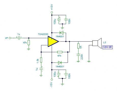
TDA 2030 audio amplifier can output 20 W but in this schematic we have reduced the power to 8w and we use 10w speakers. The input sensivity is around 200mV and the amplifier is set by the 47k and 1.5k resistors.
TDA2030 amplifier circuit diagram
(View)
View full Circuit Diagram | Comments | Reading(2013)
TDA1514 50W Hi Fi audio amplifier
Published:2012/10/11 21:18:00 Author:muriel | Keyword: TDA1514, 50W, Hi Fi, audio amplifier
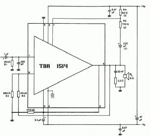
TDA1514 is a hi fi audio amplifier which can output 50W audio power. The power supply is between 10V and 30V. It can be used as a home amplifier.The TDA1514 integrated circuit is a hi-fi power amplifier for use as a building block in radio, tv and other audio applications. The TDA 1514 circuit is totally protected, also has a mute function that can be arranged for a period after power-on with a delay time fixed by external components. The device is intended for symmetrical power supplies but an asymmetrical supply may also be used. For stereo amplifier configuration use two identical circuits.
TDA1514 amplifier
(View)
View full Circuit Diagram | Comments | Reading(1736)
Stereo car audio amplifier TDA1557Q TDA1553Q
Published:2012/10/11 21:18:00 Author:muriel | Keyword: Stereo car, audio amplifier, TDA1557Q, TDA1553Q
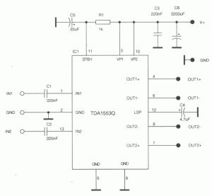
This stereo amplifier is for car purpouse and can deliver up to 2 x 22W using a single TDA1557Q or TDA1553Q from Philips.TDA1557Q TDA1553Q datasheet (View)
View full Circuit Diagram | Comments | Reading(2412)
Electronic pest (mice) repellent circuit
Published:2012/10/11 21:18:00 Author:muriel | Keyword: Electronic pest (mice), repellent
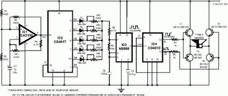
Electronic pest rat repellents emit high frequency sound waves to create an acoustically hostile environment that effectively repels rodents from protected areas. Sound is inaudible to people and non-rodent pets. It is ideal for environments were the use of poisons is inadvisable or prohibited.Beware mice, rat and mouse. It is known that a mice can hear ultrasonic sounds between 30 KHz and 50 Khz and this is pretty loud for his ears and this electronic rodent repellant does just that.
Electronic repellent circuit diagram
(View)
View full Circuit Diagram | Comments | Reading(3517)
STK4241V Home Stereo Amplifier
Published:2012/10/11 21:17:00 Author:muriel | Keyword: STK4241V, Home, Stereo Amplifier
This Home Stereo Amp is equiped with STK4241V wich is a thick film hybrid IC, AF Power Amplifier (Split Power Supply) (120W+120W min, THD = 0.08%). STK4241V has some features like:? Muting circuit built-in to isolate all types of shock noise? Current mirror circuit for low 0.08% total harmonic distortionFor this 2x120W home stereo power audio amplifier we use a single monochip STK4241V to obtain up to 120W for each channel.
STK4241V amplifier circuit diagram
(View)
View full Circuit Diagram | Comments | Reading(1657)
Infrared headphones transmitter circuit
Published:2012/10/11 21:17:00 Author:muriel | Keyword: Infrared, headphones, transmitter
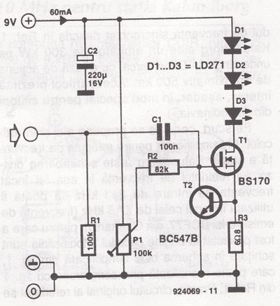
The transmitter offers a optical link (infrared) for headphones. Three infrared leds (ir) are polirised by T1 current, P1 is used to adjust the current level . Current consumption of this headphones infrared transmitter is about 60mA at 9V.Maintain separated adapter ground and audio signal ground to prevent current reactions thru LED. The optical link is relative directional and can be improved by placing the leds in different angles and placing reflectors behind them.
The optimal input audio level is 100 – 200mV for 1.2 – 2.4 m coverage of this headphones ir transmitter.On the site we provide the infrared receiver schematic for this infrared headphones transmitter.
Infrared headphones transmitter circuit
(View)
View full Circuit Diagram | Comments | Reading(1872)
Infrared headphones receiver circuit
Published:2012/10/11 21:17:00 Author:muriel | Keyword: Infrared, headphones, receiver
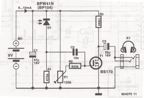
Use this infrared headphones receiver with the ir headphones transmitter.Use 600Ω headphones. BPW41N and BP104 have a filter for visible light and are centered on 950nm at 250C.At normal light illumination and 3 to 4 meters distance the audio distorsion were 1 – 2%, wich is not bad for such a simple ir headphones receiver schematic
IR headphone receiver circuit diagram
(View)
View full Circuit Diagram | Comments | Reading(1382)
Presence detector, proximity sensor circuit
Published:2012/10/11 21:16:00 Author:muriel | Keyword: Presence detector, proximity sensor
This circuit reacts in presence of any conductor object including humans. This circuit does not detect object movement but can act as an proximity sensor!Sensitivity is adjustable with P1 which will be located at a great distance from the rest of the presence detector circuit.
Presence, proximity sensor circuit diagram
(View)
View full Circuit Diagram | Comments | Reading(2923)
Audio power amplifier 50W 2N3055 MJ2955
Published:2012/10/11 21:16:00 Author:muriel | Keyword: Audio, power amplifier, 50W, 2N3055, MJ2955
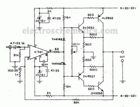
A very simple audio power amplifier circuit built with 741, 2N3053, 2N4037, 2N3055 and MJ2955 which deliver up to 50W on a 8Ω speaker.Use a 3A symmetric power supply for mono application and a 5A for stereo power amplifiers. Please take good precaution when use this audio amplifier : do not shortcircuit the output or not connect speakers ! Always check twice !
2N3055 audio amplifier circuit schematic
(View)
View full Circuit Diagram | Comments | Reading(3676)
Stun Gun Circuit schematic
Published:2012/10/11 21:15:00 Author:muriel | Keyword: Stun Gun

This is a diy simple stun gun circuit schematic ! .
DIY Stun gun circuit diagram
(View)
View full Circuit Diagram | Comments | Reading(2269)
VGA to BNC Adapter
Published:2012/10/11 21:14:00 Author:muriel | Keyword: VGA, BNC, Adapter
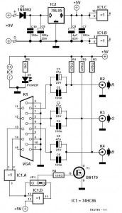
There are monitors which only have three BNC inputs and which use composite synchronisation (‘sync on green’). This circuit has been designed with these types of monitor in mind. As can be seen, the circuit has been kept very simple, but it still gives a reasonable performance.
The principle of operation is very straightforward. The RGB signals from the VGA connector are fed to three BNC connectors via AC-coupling capacitors. These have been added to stop any direct current from entering the VGA card. A pull-up resistor on the green output provides a DC offset, while a transistor (a BS170 MOSFET) can switch this output to ground.
It is possible to get synchronisation problems when the display is extremely bright, with a maximum green component. In this case the value of R2 should be reduced a little, but this has the side effect that the brightness noticeably decreases and the load on the graphics card increases. To keep the colour balance the same, the resistors for the other two colours (R1 en R3) have to be changed to the same value as R2.
VGA-BNC adapter circuit diagram
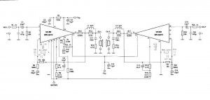
An EXOR gate from IC1 (74HC86) combines the separate V-sync and H-sync signals into a composite sync signal. Since the sync in DOS-modes is often inverted compared to the modes commonly used by Windows, the output of IC1a is inverted by IC1b. JP1 can then by used to select the correct operating mode. This jumper can be replaced by a small two-way switch, if required. This switch should be mounted directly onto the PCB, as any connecting wires will cause a lot of interference.
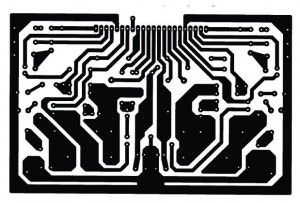
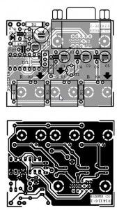
VGA to BNC adapter PCB layout
(View)
View full Circuit Diagram | Comments | Reading(2186)
Infrared alarm barrier circuit
Published:2012/10/11 21:13:00 Author:muriel | Keyword: Infrared, alarm barrier
This infrared alarm barrier can be used to detect persons passing through doorways, corridors and small gates. The transmitter emits a beam of infrared light which is invisible to the human eye. The buzzer at the output of the receiver is activated when the light beam is interrupted by a person passing through it.
Infrared Light Alarm Transmitter Circuit Schematic
Infrared Alarm Barrier Receiver Circuit Schematic
(View)
View full Circuit Diagram | Comments | Reading(2745)
VHF FM Antenna Booster Circuit
Published:2012/10/11 21:13:00 Author:muriel | Keyword: VHF, FM, Antenna Booster
Together with a good directional antenna this high performance two-stage antenna amplifier for the VHF FM broadcast band will enable you to capture far removed (DX) stations. Alternatively, it will drastically improve reception of FM signals you’ve come to accept as marginal and noisy in your area.
FM/VHF antenna amplifier circuit schematic
Together with a good directional antenna this high performance two-stage antenna amplifier for the VHF FM broadcast band will enable you to capture far removed (DX) stations. Alternatively, it will drastically improve reception of FM signals you’ve come to accept as marginal and noisy in your area.
For various reasons, an increasing number of people are not satisfied with the quality of radio signals that can be received via cable systems. Unfortunately, cross-modulation, and other nasty effects created in the head end station are in stark contrast with the superb quality of high-end FM tuners that can be bought commercially.
Not surprisingly, owners of such tuners will often prefer to have their own antenna on the roof. Add to that a high-performance FM antena booster like the one described here and you can start DXing as well as enjoying high-quality stereo reception. The author employs the present amplifier in combination with a Sangean ATS-803 World band receiver, a Philips RR-571 tuner and a single-element cubical quad directional antenna at a height of just 15 feet. Using this setup he is able to receive FM stations as far off as 500 km. (View)
View full Circuit Diagram | Comments | Reading(1617)
Magnetic field meter circuit
Published:2012/10/11 21:12:00 Author:muriel | Keyword: Magnetic, field meter
These days when electronic circuits can be found almost anywhere, there is, some people fear*, a different kind of environmental pollution. They call it electrosmog (the word does not appear in any dictionary – not even technical ones), but in this article we will call it stray magnetic fields (SMFs). Some ‘experts’ think that SMFs may affect the physical well-being of people. If you believe that these experts are right, the magnetic-field meter described will help you find sources of SMFs and determine their strength. These findings may help you reduce the fieldstrength.
The input amplifier, based on IC1a, ensures that the signal from the induction coil, L1, is amplified x 101. The coil is terminated into a high impedance, so that its output is buffered by the op amp. The integrator consists of IC1B, another of the four op amps contained in IC1.The (active) rectifier, based on IC1c, is, in fact, a differential amplifier that lessens the average voltage by the output potential of the integrator. Since the op amp is powered asymmetrically, the output is a half-wave rectified alternating voltage. This voltage is averaged by R16-C6 or, in case a DVM is used as the meter, by R18-R20- C7. The form factor (2.22) is corrected by the rectifier. The level matching is purposely carried out by the rectifier since this op amp has a much larger swing than IC1a or IC1b.
Magnetic field meter circuit design
The principle of the present meter is shown in the block diagram in Figure 1. The induction coil used to detect the magnetic field is represented by an alternating- voltage source, V1, whose average output is 1 μV. The output of the source is amplified x 101 by op amp X1. The op amp is linked to integrator X2 which provides frequency-dependent amplification. For direct-voltage signals this is 1000, for high-frequency signals it is 0. The cross-over frequency is chosen so that the amplification is uniform over the range in which magnetic induction is to be measured (40 Hz – 10 kHz). Feedback network R4-R6 automatically ensures that the circuit has a stable d.c. operating point at all times. This makes it possible for relatively inexpensive op amps to be used. Also, the internal attenuator ensures that the maximum d.c. amplification is x 101 (1+R6/R5). The value of R6/R5 also determines the lower limit of the frequency range.
Magnetic-field meter circuit diagram
The circuit diagram of the meter is shown in Figure 2. It consists of an input amplifier, integrator, automatic offset correction network, rectifier with d.c. suppression, display and associated drive, power supply, and a socket for connection to a digital voltmeter (DVM).
Op amps IC1a and IC1b carry a pure sinusoidal signal that alternates symmetrically around a direct voltage of 3 V, whereas that of IC1c alternates around 0 V. This means that this op amp can handle an amplification of x 2.2 much better than the earlier two. The drop across C6 is used by the display driver, IC2, to represent the strength of the magnetic field. The driver has its own reference-voltage source. This 1.25 V source is also used to derive an auxiliary voltage for op amps IC1a and IC1b. The potential at node A is [ ( R14 + R15 ) / R15 ] x 1.25 = 3 V.
The minimum voltage at which IC2 provide full drive is 1.2 V. Since the IC is driven by an averaged potential, the signal level required for full drive is 1.2 x Pi = 3.77 Vpp. Because the signal amplification takes place in the rectifier, that is, the op amp with the largest drive range, a drop in battery voltage does not immediately affect the accuracy of the meter. The (View)
View full Circuit Diagram | Comments | Reading(2048)
Digital Potentiometer circuit
Published:2012/10/11 21:12:00 Author:muriel | Keyword: Digital Potentiometer
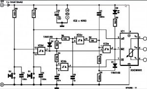
Xicor’s digitally controlled E2POT ICs provide ergonomic and long-lasting alternatives to mechanical potentiometers. The ICs in the X9CMME series have a 7-bit counter with reversible count direction and a decoder that enables one of the 100 analogue switches.The outputs of the analogue switches serve as the wiper of a potentiometer, while the inputs are linked to a potential divider composed of 99 equal resistors. The counter state may be stored in a non-volatile EEPROM, so that it can serve as the output value at a subsequent start.
The X9CMM series is designed to operate from 5 V supply lines. The potential across the resistive divider must not exceed 10 V (only 4 V in case of the X9C102). The ON resistance of the analogue switch is about 40 Ohm, so that the current through the wiper is limited to 1 mA.
E2POT ICs have three inputs for the digital drive. The level at U/D determines whether a trailing edge at clock input /INC lowers or raises the counter state. This action only takes place if chip select input /INC is low. A leading edge at CS arranges for the counter state to be stored when /INC is high. When /INC is high, the IC is in the standby mode.
Digital potentiometer circuits diagram
The circuit diagram shows a complete digital potentiometer based on a Type X9CMME. It is provided with two controls, S1 and S2, an optical indicator and a delayed frequency change-over of the clock generator. When keys S1 and S2 are open, resistors R8 and R9 hold the inputs of IC2d, a NAND, as well as the U/D input of IC1 high. The low level at the output of IC2d disables clock generator IC2a. Frequency determining capacitor C1 is discharged in the quiescent state.
When one of the keys is pressed (S1 firmly, S2 gently), the output of IC2d changes state, so that the clock generator and IC1 (via IC2b) are enabled. Capacitor C1 is then charged via R1 and R2 until the input level of IC2a goes low, whereupon the gate output linked to the clock input of IC1 changes state (from low to high). When this happens, C1 is discharged via R1 and D1 until the upper trigger level of IC2a is attained. The gate then changes state again and the above action repeats itself. The clock signal is optically monitored by D3.
When the output of IC2c is high, the gate draws a portion of the charging current from C1, which results in the clock frequency at /INC being relatively low. At the same time that the generator is enabled, C6 begins to be charged gradually via R6 and R7 until IC2c changes states (from high to low). Circuit IC2 then contributes to the charging current to C1, whereupon the clock frequency increases: in the prototype, the frequency rose in four seconds from 1.3 Hz to 3.1 Hz. When the keys are released, the clock generator stops. At the same time, C6 is discharged rapidly via R6 and D2, so that the frequency is low again when the keys are operated anew.The switch-off delay owing to R4-C2 enables the actual counter state to be stored by the internal logic. The circuit draws a current of 0.3-1.0 mA. (View)
View full Circuit Diagram | Comments | Reading(2108)
Wideband VHF preamplifier
Published:2012/10/11 21:11:00 Author:muriel | Keyword: Wideband, VHF, preamplifier
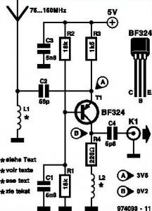
This inexpensive VHF preamplifier uses the BF324 TO92 style pnp transistor in a grounded-base configuration. The circuit may be used as a signal booster with VHF receivers whose front end suffers from low sensitivity (such as many valved and army surplus types). The frequency range of the preamplifier is roughly from 75MHz to 150MHz. The two inductors in the circuit are home made. L1 consists of 10turns of 24SWG enamelled copper wire; the internal diameter is 3mm, no core. Inductor L2 has 13 turns of the same wire, and an internal diameter of 5mm; no core is used either. A construction tip: close-wind the inductors using 3 and 5mm drill bits respectively as temporary formers.
The prototype of the preamplifier was successfully used with an 88-108 MHz FM broadcast receiver and a 2-metre VHF ham receiver. The preamplifier draws about 2.5mA from a 5-volt supply.
Wideband VHF preamplifier circuit schematic
(View)
View full Circuit Diagram | Comments | Reading(3190)
Single-Chip VHF RF Preamplifier
Published:2012/10/11 21:10:00 Author:muriel | Keyword: Single-Chip, VHF, RF, Preamplifier
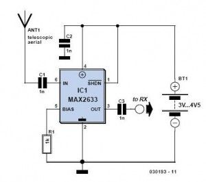
Here is a high performance RF amplifier for the entire VHF broadcast and PMR band (100-175 MHz) which can be successfully built without any special test equipment. The grounded-gate configuration is inherently stable without any neutralization if appropriate PCB layout techniques are employed. The performance of the amplifier is quite good.
The noise figure is below 2 dB and the gain is over 13 dB. The low noise figure and good gain will help car radios or home stereo receivers pick up the lower-power local or campus radio stations, or distant amateur VHF stations in the 2-metres band. Due to the so-called threshold effect, FM receivers loose signals abruptly so if your favourite station fades in and out as you drive, this amplifier can cause a dramatic improvement.
The MAX2633 is a low-voltage, low-noise amplifier for use from VHF to SHF frequencies. Operating from a single +2.7 V to +5.5V supply, it has a virtually flat gain response to 900 MHz. Its low noise figure and low supply current makes it ideal for RF receive, buffer and transmit applications. The MAX2633 is biased internally and has a user-selectable supply current, which can be adjusted by adding a single external resistor (here, R1). This circuit draws only 3 mA current.
VHF RF preamplifier circuit diagram
Besides a single bias resistor, the only external components needed for the MAX2630 family of RF amplifiers are input and output blocking capacitors, C1 and C3, and a VCC bypass capacitor, C2. The coupling capacitors must be large enough to contribute negligible reactance in a 50-Ω system at the lowest operating frequency. Use the following equation to calculate their minimum value:Cc = 53000/ flow [pF]
(View)
View full Circuit Diagram | Comments | Reading(1317)
| Pages:305/2234 At 20301302303304305306307308309310311312313314315316317318319320Under 20 |
Circuit Categories
power supply circuit
Amplifier Circuit
Basic Circuit
LED and Light Circuit
Sensor Circuit
Signal Processing
Electrical Equipment Circuit
Control Circuit
Remote Control Circuit
A/D-D/A Converter Circuit
Audio Circuit
Measuring and Test Circuit
Communication Circuit
Computer-Related Circuit
555 Circuit
Automotive Circuit
Repairing Circuit