
Circuit Diagram
Index 314
Battery Guard for Emergency Lights
Published:2012/9/28 21:01:00 Author:muriel | Keyword: Battery Guard, Emergency Lights
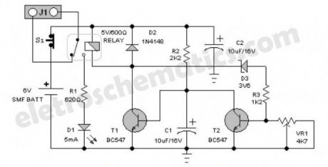
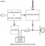
As the name implies,emergency light is a source of light available during an emergency.It is an automatic system in which a rechargeable battery operated light source turns on as soon as the ac mains fail.When the grid supply is restored,the lamp is turned off. An emergency light essentially consists of a source of electricity – a rechargeable battery pack and an automatic sensing circuit to check the presence(or absence) of mains supply.The sensing circuit connects a lamp (or a compact fluorescent tube inverter) circuit in the event of mains failure and disconnects it when the mains supply is restored.When ac mains supply is available,a charger circuit charges the battery pack to keep it in top condition(fig 2).
Emergency Lights Guard Circuit Diagram
Over the years,emergency lights have become better designed and more reliable. However, they retain a few weak facilities. Usually 6 volt sealed maintenance free (SMF) batteries are used in portable emergency lights. Unfortunately, many low cost lights give no indication when the battery has gone flat, so that there is a risk of the battery failure. Only high-end systems have built in electronic deep discharge protection circuitry to disconnect the output load in case the battery voltage happens to fall below a safe value.
(View)
View full Circuit Diagram | Comments | Reading(1842)
Voltage and Current Tester
Published:2012/9/28 21:00:00 Author:muriel | Keyword: Voltage, Current, Tester
This Simple Voltage and Current tester can be used to measure the forward Voltage drop and current through Semiconductor Diodes like LED, Infrared diode, Photo diodes, Silicon diodes etc. This is ideal to assess the voltage and current drops through these devices during circuit design and calculating the power consumption in a particular section of the circuit. Different types of LEDs including power LEDs are now used in various applications. The voltage rating of these devices range between 1.8 to 5 volts. Current rating also varies from 20 mA to 50 mA. So by assessing the actual voltage and current consumption, it is easy to get full brightness without damaging the device. This will also prevents the unnecessary heating of these delicate devices and their breakdown
Voltage and Current Tester circuit
The circuit is a current regulator using the Darlington PNP transistor BD 140. It provides 9 volts and around 50 mA current to the device under test. Switch S1 is used to select the Voltage and current measurement. If S1 is placed in position 1, the circuit measures the current drop across the device under test. A 100 mA meter is placed in series with the current path. So that when the device is connected to point A and B, meter shows the current flowing through the device
When S1 is placed in position 2 and the device is connected to points A and B, voltage drop in the device can be measured. The 0-30 Volt meter is connected parallel to the device under test. So that it can give the voltage drop across the device.
Since diodes are One-way conductors, observe polarity while connecting to points A and B. Anode should be in A and Cathode in B. Connect small Alligator Clips to points A and B to hold the device under test.
Volt and Ampere Meter
Types of Diodes
(View)
View full Circuit Diagram | Comments | Reading(1956)
Improved Infrared Detector circuit
Published:2012/9/28 21:00:00 Author:muriel | Keyword: Improved, Infrared Detector
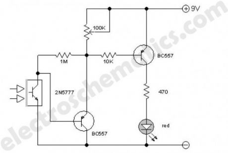
This improved infrared detector is specifically intended for use with commercial IR remote control handsets. This little circuit is useful for quick go/no-go testing of just about any remote control transmitting Infrared (IR) light signal. The key component of the IR detector is a sensitive photo transistor 2N5777. All infrared remote controls transmit pulse bursts. The photo transistor detects the modulated IR signal from the remote control handset under test and its output is processed by next BC557 and fed to the final LED driver transistor BC557. As a result the red LED in the circuit starts blinking in tune with the received signal. Please note that the LED lights up constantly when day light or other source of continuos IR light is detected.
Infrared Detector Circuit Diagram
The infrared detector circuit may be powered by just about any standard 9V compact battery or a wall adaptor capable of supplying 9VDC at about 100mA.The only setting up required is to adjust the 100K variable resistor.The construction drawing shows how the circuit may be cased in a small ABS case.
Block Diagram of the IR detector
(View)
View full Circuit Diagram | Comments | Reading(1973)
Dual Power source circuit
Published:2012/9/28 21:00:00 Author:muriel | Keyword: Dual, Power source
Here is a Dual power source for the Home Security system which has to be switched on continuously. It is a power saving circuit that uses a Solar panel for providing power during day time and a transformer power supply during night.It has a battery backup and the power to the security system is derived from the 12 Volt 4.5 Ah battery.So that even if the day light is not sufficient in clody days, the security system will work normally. About the Solar Power sourceDuring day time, the security system gets 12 volt power supply from the battery or the Solar Panel. If the amount of power from the solar panel is not sufficient, battery will compensate it. Typically a single solar cell generates 0.5 volt and around 50 mA current in bright light. A single solar cell is rated at 45 mW. So in the 12 volt solar panel, there will be 24 solar cells connected serially. It can give 1 Ampere current in day light. Typically a 15 W Solar panel gives 1 Ampere current in bright light. Here a 12 V 5W Solar panel is used in the circuit to give power to the security system and charging current to the battery. It gives around 300 mA current.
About the DC power source
Night charging is attained by the 12 volt DC obtained from a 0-12 volt 1 Amps step down transformer and the fullwave rectifier comprising D3 through D6. Capacitor C2 removes ripples from DC to give clean power to the security system and for the battery.Resistor R4 gives 80 mA current during night for Trickle charging the battery.At the same time, power to the security system will be available from the battery. The trickle charging provision save AC power and protect battery from over charging since the battery will get sufficient charge during day time.
Dual Power source Circuit diagram
Battery status indicator
This part of the circuit indicates the voltage level in the battery as well as the voltage from the solar panel.Zenerdiode ZD conducts only when the battery holds more than 11.6 volts. When ZD conducts Red LED illuminates.When the battery voltage goes below 11 volts ,LED turns off.If the LED is not lighting, it indicates that battery is not attaining full charge or the solar panel is not giving 12 volts.
LDR switch
This is used to switch on the DC power from the transformer power supply at night. LDR offers low resistance in day light so that it gives more current to the base of T1.It is a PNP transistor and it remains off during day time due high voltage in its base. T2 also remains off due the lack of base bias. During night,resistance of LDR decreases, and the base of T1 becomes negative. It then turns on. T2 also turns on and charging current is available from the emitter of T2. Resistor R4 reduces the charging current to 80 mA for trickle charging the battery. Adjust VR1 to set the sensitivity of LDR.
BD139 and BC557 Pin connections
(View)
View full Circuit Diagram | Comments | Reading(1343)
Smart smoke sensor alarm circuit
Published:2012/9/28 20:59:00 Author:muriel | Keyword: Smart smoke, sensor, alarm
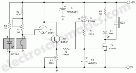
At the heart of this ultra simple smoke sensor or detector alarm is H21A1, which is a photo-interrupter module consists of a gallium-arsenide infrared LED coupled to a silicon phototransistor in a plastic housing. The slot between the infrared sender(LED) and receiver (phototransistor) allows interruption of the signal with smoke, switching the module output from ‘on’ to ‘off’.When the smoke enters the slot, the infrared beam falling on the phototransistor is obstructed. As a result, the phototransistor stops working and the transistors (T1&T2), wired as a simple darlington pair, conduct to activate the rest of the circuit.
When the darlington pair conducts, the gate voltage of SCR BT169 (T3) goes high and the SCR is fired. Consequently, the gate terminal of mosfet BS170 (T4) receives positive voltage through resistor R4 and the active piezo-sounder (BZ1) energises to latch! Visual indicator LED (D1) lights up instantly. The buzzer sounds to indicate the presence of smoke, unless you switch off the circuit by disconnecting the 9 volt dc input supply. For optimum performance, adjust trimpots P1, P2 and the value of resistor R1.
Smoke detector alarm circuit diagram
H21A1 schematic
(View)
View full Circuit Diagram | Comments | Reading(3296)
Entry Alarm circuit
Published:2012/9/28 20:58:00 Author:muriel | Keyword: Entry, Alarm circuit
This is an Infrared based Brocken beam alarm to protect doors and entry passages. It gives a loud alarm when somebody crosses the Invisible Infrared barrier. It can protect the doors both day and night and is free from false triggering. The circuit is too simple and can be a good evening project for the hobbyists. The circuit uses Infrared diodes to emit continuous IR rays which are not pulsed as in the case of remote handsets. The NPN Darlington Photo transistor is used as a light sensor. L14F1 is the ultra sensitive Darlington photo transistor with high gain. Its collector is connected to the positive rail through VR1 and the Emitter has a Green LED to indicate standby mode. The base of T1 is left free without connecting anywhere. This base junction is exposed through the window of T1 so that light photons will bias the base.
The degree of biasing depends on the intensity of photons.T2 is the alarm driver and its base is connected to the collector of T1.So that the base bias of T2 depends on the conduction of T1. When the Infrared rays illuminate the photo transistor, it conducts pulling the base of T1 to ground level so that it remains off. Red LED and Buzzer connected to the emitter of T2 remains off in this condition. When a person crosses the IR beam, T1 turns off and its collector voltage becomes high. T2 then conducts and activates Red LED and buzzer.L14F1 DatasheetBC547 Datasheet
Entry Alarm Circuit diagram
The circuit can be constructed on a small piece of Perf board. Assemble R1 and IR LEDs on a separate board. Fix IR LEDs on one side of the entry and the Phototransistor on the opposite side. Carefully align IR beam on the Phototransistor so that buzzer will be silent in the standby mode. Move hand across the beam, buzzer should sound.VR1 adjust the base bias of T2 to keep the buzzer off in the standby mode.
L14F1 Phototransitor
L14F1 and BC547 Pins
(View)
View full Circuit Diagram | Comments | Reading(1042)
Fast Charger circuit
Published:2012/9/28 20:57:00 Author:muriel | Keyword: Fast Charger
Here is a High current charger for Fast charging sealed lead acid batteries used in Automobiles, Inverters etc. This charger can give 5 Ampere current for quick rejuvenation of the battery. It uses an Adjustable voltage regulator so that 6 volt and 12 volt batteries can be charged.LM338K is a high current variable voltage regulator that can provide 2 to 25 volts DC with high current output. It’s important features are 7 Ampere peak output current, adjustable output down to 1.2 volts, thermal regulation etc. It is easy to use and require only 2 external resistors to set the output voltage. The time dependent current limiting ability of the device allows peak current of up to 12 ampere to be drawn for short time. So that it is useful in heavy transient loads and speed start up.
LM 338 Variable Regulator
Design considerations
Use of external resistorsLM338 K is available in metal can package TO3. K suffix metal can. It has only two pins – Vin and Adjust. The body of the device acts as the output pin. On the bottom side, the first pin is adjust and the second pin is Vin. LM338 requires heat sink to dissipate heat since it is draining high current. Two resistors are required to set the output voltage. Resistor R1 (220 Ohms) act as the programme resistor. Usually 1.25 volts reference voltage (Vref) develops between the output and adjusts pins. The reference voltage is impressed across the programme resistor R1.The voltage across R1 is constant so that constant current flows through the output set resistor VR1.Therefore output voltage is
Vout = Vref (1 + VR1 / R1) + I Adj VR1
Use of capacitorsTwo capacitors are usually soldered close to the input and output terminals. C2 is the input bypass capacitor. Output capacitor C3 gives stability for the output current.
Circuit operationInput voltage is obtained from a 15-0-15 volt 5 Ampere secondary transformer with rectifying diodes D1 and D2. Capacitor C1 makes the DC ripples free and around 16 volt DC enters into the Vin input of the regulator. VR1 can be used to set the output voltage from 2 volts to 25 volts. A digital panel meter is used for measuring the output voltage. Ready made LED or LCD panel meters are available at reasonable cost. This can be directly connected to the output. So by adjusting VR1, it is easy to see the output voltage in the meter .If the output put voltage reduces due to line voltage drop, it can be easily detected through the panel meter. The panel meter also can be used to measure the terminal voltage of the battery. If the power supply is switched off, meter shows the terminal voltage. If the voltage remains steady, it indicates that the battery is fully charged and holding charge.Easily available IN 5402 diodes are rated at 3 Amps so if the device become too hot, use a 10 A KBPC 1000 Bridge rectifier.
Fast Charger Circuit diagram
(View)
View full Circuit Diagram | Comments | Reading(1336)
Timer light switch circuit
Published:2012/9/28 20:57:00 Author:muriel | Keyword: Timer, light, switch
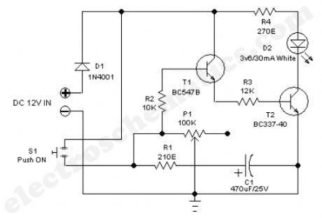
Tiny Timer Light Switch presented here is a simple transistorised electronic timer which drives a high efficiency white LED for a finite time out. This circuit is very useful for in-car reading etc. The circuit works off 12 volt dc supply. After construction, fit the unit at a suitable location inside your car and power the circuit from the in-dash standard cigar lighter socket. The timer light switch is ultra simple, economic, straight forward and self explanatory. How the timer light switch works?Normally T1 is turned off by P1 and R2. When the trigger switch S1 is pressed the base of T1 is connected to the +12V supply via R2. Now T1 turns on and this action turns on the next transistor T2 which in turn energises the white LED (D2). Resistor R4 limits the operating current of white LED (D2).
When the switch is pressed is current also flows into capacitor C1 (through R1) and charges it. So when the switch S1 is released the charge in the capacitor C1 keeps T1 turned on until the charge has decayed away through R2 and P1. You can easily increase the ouput on time by increasing the resistance of the potentiometer P1.
Timer Light Switch Circuit Diagram
(View)
View full Circuit Diagram | Comments | Reading(1968)
LED Tools
Published:2012/9/28 20:57:00 Author:muriel | Keyword: LED, Tools
Here are two simple tools for the Hobbyists to check their Prototype boards. These use LEDs as visual indicators for the quick check reducing the job of multimeter testing
Continuity TesterThis can be used to check the continuity of PCB tracks, wires, transformer windings, fuse, diodes, resistors etc. It uses a Red LED to give the positive indication. If the continuity exists, current flows through the probes and LED lights.
Continuity Tester Circuit
Polarity Tester
This simple LED tool indicates the polarity of connections. It uses a bicolour LED to give two indications. If the polarity is correct, Green LED lights, and if polarity is reversed, Red LED lights.
Polarity Indicator Circuit
(View)
View full Circuit Diagram | Comments | Reading(1522)
Short Circuit Indicator
Published:2012/9/28 20:57:00 Author:muriel | Keyword: Short Circuit, Indicator
Here is a valuable Add on circuit to save electronic components in the assembled board from damage. It gives warning beep if there is a short circuit in the assembled board. Thus it helps to switch off the power supply immediately to save valuable components. If the circuit board is OK, Green LED lights indicating that power supply is normal. If there is a short in the PCB tracks or pins of components, Green LED turns off and Buzzer sounds indicating the short circuit. The circuit uses two NPN transistors BC 547 to sense the short circuit. If the assembled board is normal, current flows from the power supply through polarity protecting diode D1. The Assembled board gets power and Green LED lights. At the same time T2 forward bias and its collector goes to ground potential. This makes T1 off due the absence of base bias. Buzzer and Red LED connected to the collector of T1 remains off. If there is a short circuit in the board under test, D2 reverse biases and T2 turns off. Now the base of T1 becomes high and it conducts. This turns on Buzzer and Red LED to indicate short circuit.
Short Circuit Indicator Circuit diagram
Connect the circuit to the output of the Power supply observing polarity.Output of the circuit is used to power the circuit board under test. (View)
View full Circuit Diagram | Comments | Reading(834)
Telephone Lamp Circuit
Published:2012/9/28 20:56:00 Author:muriel | Keyword: Telephone, Lamp Circuit
Here is a White LED Lamp that turns on when the telephone rings. The cool white light helps to locate the phone in darkness and also helps to note the message or telephone number. The lamp remains on for three minutes then turns off.The telephone lamp circuit is powered by a 9 volt PP3 battery and connected to the telephone lines. Capacitors C1,C2 and resistors R1 and R2 converts AC signals to DC to trigger the NPN transistor T1.When the phone is on hook, there will be around 48 volts in the lines which reduces to 12 volts when the phone is Off hook. Capacitor C1 and C2 reduces the line voltage to low value DC and diode D1 rectify the AC signals.
Telephone Lamp Circuit diagram
The lamp circuit is built around the timer IC555. It is designed as a monostable timer to turn on the White LEDs for three minutes. Resistor R6 and capacitor C4 determines the time delay. When the telephone rings, transistor T1 triggers and its collector turns low. This triggers the monostable and its output becomes high to switch on the White LEDs.
BC547 Pin connection
(View)
View full Circuit Diagram | Comments | Reading(1392)
Transformerless Power Supply 30V 1A
Published:2012/9/28 20:56:00 Author:muriel | Keyword: Transformerless, Power Supply, 30V, 1A
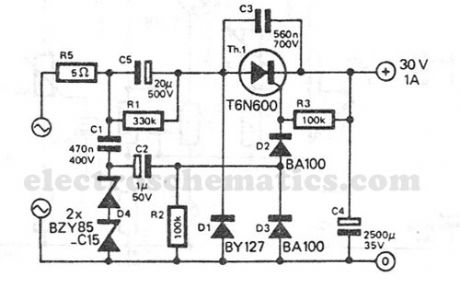
This transformerless power supply circuit is designed for medium current applications. During the negative half period, the capacitor C5 is charged to peak voltage network.
Transformerless Power Supply Circuit Schematic
The positive half wave will open the thyristor and the electric charge accumulated in C5 will be transferred in C4. The transport of electric charge through the thyristor begins when the voltage on C4 drop below a specified level of voltage (set by zener D4). Thus the output voltage does not depend too much on the voltage variations or the output load.
The thyristor control signal is obtained as follows: main sinusoidal voltage is applied through capacitor C1 to D4 zener diodes that limit the voltage to 30 Vpp. Thyristor will trigger on the first front of the limited voltage that is applied through C2 – R2. (View)
View full Circuit Diagram | Comments | Reading(3982)
Multiplexer Switch circuit with 4066
Published:2012/9/28 20:56:00 Author:muriel | Keyword: Multiplexer, Switch circuit,4066

This multiplexer switch circuit is built with the IC 4066 and was designed to switch multiple signal sources into a single common output and can be used as a replacement for the conventional mechanical switches.Conventional multiplexer switches hava an annoying disadvantage that the video signals mix over when the source is changed but this circuit avoids this problem by disabling the inactive signal line.The heart of the switch is a digitally controlled analog switch 4066. The switches are ES1 … ES8 and each 4066 contains 4 switches. When channel 1 is selected, ES1 and ES2 are closed and ES3 is open. Channel is suppressed at this moment since ES5 and ES6 are open and ES7 prevents cross-over between the two channels by grounding the channel 2 line.
The bandwidth of the multiplexer sw circuit is around 8 MHz. The current consumption is 1 mA. A high level power supply voltage level is required since the input impedance level of the circuit drops with higher voltage levels.
When the multiplexer circuit is connected to a 75 Ω impedance load, some signal losses will result due to the internal resistance of the switches. This can be compensated by connecting a video amplifier at the output.Article submitted by Michael Gregory – Romania.
Multiplexer Switch Circuit Diagram
(View)
View full Circuit Diagram | Comments | Reading(2518)
MAX9730 2.4W Class G Power Amplifier
Published:2012/9/28 20:52:00 Author:muriel | Keyword: MAX9730, 2.4W, Class G, Power Amplifier

The MAX9730 features a mono Class G power amplifier with an integrated inverting charge-pump power supply. The charge pump can supply up to 500mA of peak output current over a 2.7VDC to 5.5VDC supply voltage range, guaranteeing up to 2.4W output power into an 8Ω load. The 2.4W output power allows for transient audio content to remain unclipped as the battery rail collapses over time. The MAX9730 maximizes battery life by offering high performance efficiency. Maxim’s proprietary output stage provides efficiency levels greater than Class AB devices without the EMI penalties commonly associated with Class D amplifiers. High efficiency allows the MAX9730 to be packaged in a WLP package without derating the output power handling capability.The device utilizes fully differential inputs and outputs, comprehensive click-and-pop suppression, shutdown control, and soft-start circuitry. The MAX9730 is fully specified over the -40°C to +85°C extended temperature range and is available in ultra-small, lead-free, 20-bump WLP (2mm x 2.5mm) and 28-pin TQFN (4mm x 4mm) packages.Download the MAX9730 datasheet…
MAX9730 Typical Application
(View)
View full Circuit Diagram | Comments | Reading(1532)
1 Watt Four Stage FM Transmitter
Published:2012/9/28 20:52:00 Author:muriel | Keyword: 1 Watt, Four Stage, FM Transmitter
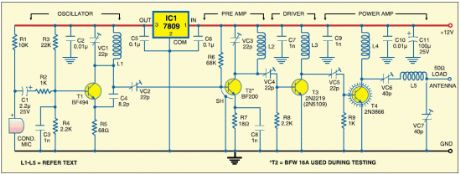
This FM transmitter circuit uses four radio frequency stages: a VHF oscillator built around transistor BF494 (T1), a preamplifier built around transistor BF200 (T2), a driver built around transistor 2N2219 (T3) and a power amplifier built around transistor 2N3866 (T4). A condenser microphone is connected at the input of the oscillator. Working of the 1 Watt transmitter circuit is simple. When you speak near the microphone, frequency-modulated signals are obtained at the collector of oscillator transistor T1.
The FM signals are amplified by the VHF preamplifier and the pre-driver stage. You can also use transistor 2N5109 in place of 2N2219. The preamplifier is a tuned class-A RF amplifier and the driver is a class-C amplifier. Signals are finally fed to the class-C RF power amplifier, which delivers RF power to a 50-ohm horizontal dipole or ground plane antenna.
Use a heat-sink with transistor 2N3866 for heat dissipation (Note: or 2N4427 because it works better at 12 V and delivers up to 1 watt RF power). Carefully adjust trimmer VC1 connected across L1 to generate frequency within 88-108 MHz. Also adjust trimmers VC2 through VC7 to get maximum output at maximum range.
Regulator IC 78C09 provides stable 9V supply to the oscillator, so variation in the supply voltage will not affect the frequency generated. You can also use a 12V battery to power the circuit. Assemble the circuit on a general purpose PCB. Install the antenna properly for maximum range.
Coils L1 through L5 are made with 20 SWG copper-enamelled wire wound over air-cores having 8mm diameter. They have 4, 6, 6, 5 and 7 turns of wire, respectively.
Source: Electronics For You Magazine http://www.electronicsforu.com/electronicsforu/lab/freecircuitslist.asp?id=464&title=Four-Stage%20FM%20Transmitter
Note: This transmitter is meant only for educational purposes. use of this transmitter with outdoor antenna is illegal in most parts of the world.
FM Transmitter circuit diagram
(View)
View full Circuit Diagram | Comments | Reading(1349)
220V LED Flasher circuit
Published:2012/9/28 20:52:00 Author:muriel | Keyword: 220V, LED, Flasher
This is an AC powered LED flasher that can drive two High bright LEDs directly from the power obtained from the AC lines. The high bright LED flasher can be used as a Mock flasher or as an ornamental LED.
AC voltage is rectified by the full wave rectifier formed of D1 through D4.The rectified voltage is reduced to a safer level by the resistor R1.The low volt DC is then made ripple free by C1 and regulated to 5 volt DC by the Zener diode ZD. Transistor T1 and T2 form an oscillator with capacitor C3 and resistor R2. The charging and discharging of C3 through R2 makes T1 and T2 oscillating.LED connected to the positive of C5 flashes depending on the charge and discharge of C5.When C3 fully charges, T1 conducts and its collector pulls the base of T2 to ground and it also conducts. This causes the discharge of C5. When C3 discharges, T1 and T2 turns off and now C5 charges through R4.This causes the Flashing of LED.
LED Flasher Circuit diagram
(View)
View full Circuit Diagram | Comments | Reading(1918)
Precision Monostable circuit
Published:2012/9/28 20:51:00 Author:muriel | Keyword: Precision, Monostable circuit
Here is a Monostable Multivibrator using IC CD4538. It is a Precision Monostable / Astable Multivibrator IC free from false triggering. This can be used for various application in which precise timing cycle is requiredCD 4538 is the Precision Monostable /Astable Multivibrator IC that is free from False triggering. It is more reliable than the popular timer IC 555. Here the IC is wired as a short duration monostable timer using R1 and C1 as timing components. With the given values, output of IC1 remains low for three minutes. By changing the value of C1 or R1 various time intervals can be obtained.
Unlike 555 IC in the monostable mode, here in CD4530, output of IC becomes high at power on and becomes low when the trigger pin5 gets a low-to-high transition pulse. When S1 is pressed, the high going pulse triggers IC and its output goes low. This drives the load through the PNP transistor T1.Load can be an LED, Buzzer etc.
Precision Monostable Circuit diagram
CD4538 Pin connection
(View)
View full Circuit Diagram | Comments | Reading(917)
Infrared Switch circuit
Published:2012/9/28 20:50:00 Author:muriel | Keyword: Infrared, Switch
Here is a Simple Infrared controlled Switch. It can be operated using the TV remote handset.The Load can be any AC operated device which can be connected to the relay. The load turns on for three minutes then goes off. It can be used to switch on the lamp in the TV roomThe circuit uses the popular IR sensor module TSOP 1738 and the precision Monostable / Astable IC CD4538. TSOP 1738 IR sensor accepts 38 KHz infrared pulses from the remote. Its output is high at power on and gives 5 volts. When it senses pulsed IR rays, its output becomes low.
IR Switch Circuit diagram
CD4538 is the Precision Monostable /Astable Multivibrator IC that is free from false triggering. It is more reliable than the popular timer IC 555. Here the IC1 is wired as a short duration monostable timer using R3 and C1 as timing components. With the given values, output of IC1 remains low for three minutes. By changing the value of C1 or R3 various time intervals can be obtained. Unlike 555 IC in the monostable mode, here in CD4530, output of IC becomes high at power on and becomes low when the trigger pin5 gets a low-to-high transition pulse. (View)
View full Circuit Diagram | Comments | Reading(1057)
LA4440 Stereo Amplifier circuit
Published:2012/9/28 20:50:00 Author:muriel | Keyword: LA4440,Stereo Amplifier
LA4440 is a two channel audio power amplifier IC with inbuilt in dual channels enables it for stereo and bridge amplifier applications. In dual mode it gives 6 W per channel and in bridge mode 19 W output.
It has good ripple rejection of 46dB, small residual noise, built in over voltage and surge voltage protection etc. ideal feature of the IC is its pin-to-pin protection. Here LA4440 is wired in Stereo configuration using both inputs and outputs.
Features of LA4440
1. Built in two channels to use as Mono and Stereo2. Dual mode 6W x 2 and Bridge mode 19W3. 46 dB Ripple rejection4. 18V Max. Power handling and 12V typical5. Good channel separation and low distortion6. Built in Audio Muting function and Pin-to-Pin protection7. Surge protection circuitry
LA4440 Stereo Amplifier Circuit
(View)
View full Circuit Diagram | Comments | Reading(1772)
Numeric Water Level Indicator circuit
Published:2012/9/28 20:49:00 Author:muriel | Keyword: Numeric, Water Level Indicator

Most water-level indicators for water tanks are based upon the number of LEDs that glow to indicate the corresponding level of water in the container. Here we present a digital version of the water-level indicator. It uses a 7-segment display to show the water level in numeric form from 0 to 9.The numeric water level indicator circuit works off 5V regulated power supply. It is built around priority encoder IC 74HC147 (IC1), BCD-to-7-segment decoder IC CD4511 (IC2), 7-segment display LTS543 (DIS1) and a few discrete components.
When the water tank is empty, all the inputs of IC1 remain high. As a result, its output also remains high, making all the inputs of IC2 low. Display LTS543 at this stage shows ‘0,’ which means the tank is empty. Similarly, when the water level reaches L-1 position, the display shows ‘1,’ and when the water level reaches L-8 position, the display shows ‘8.’ Finally, when the tank is full, all the inputs of IC1 become low and its output goes low to make all the inputs of IC2 high. Display LTS543 now shows ‘9,’ which means the tank is full.
Assemble the numeric water level circuit on a general-purpose PCB and enclose in a box. Mount 7-segment LTS543 on the front panel of the box. For sensors L-1 though L-9 and ground, use corrosion free conductive-metal (stainless-steel) strips.Source: Electronics For You Magazine
Numeric Water-Level Indicator Circuit Diagram
(View)
View full Circuit Diagram | Comments | Reading(3788)
| Pages:314/2234 At 20301302303304305306307308309310311312313314315316317318319320Under 20 |
Circuit Categories
power supply circuit
Amplifier Circuit
Basic Circuit
LED and Light Circuit
Sensor Circuit
Signal Processing
Electrical Equipment Circuit
Control Circuit
Remote Control Circuit
A/D-D/A Converter Circuit
Audio Circuit
Measuring and Test Circuit
Communication Circuit
Computer-Related Circuit
555 Circuit
Automotive Circuit
Repairing Circuit