
Circuit Diagram
Index 316
Pulse generator circuit with 555
Published:2012/9/27 21:33:00 Author:muriel | Keyword: Pulse generator, 555
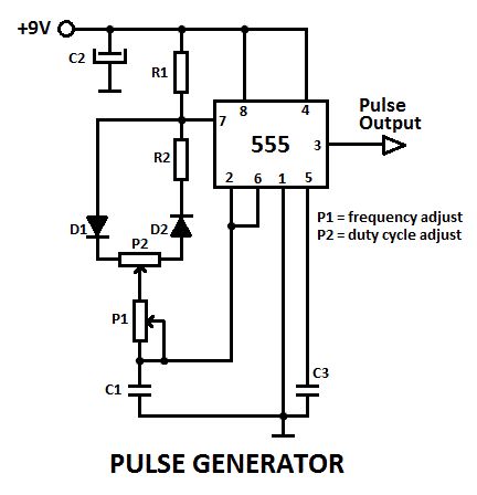
This is a pulse generator with adjustable duty cycle made with the 555 timer IC. The circuit is an astable multivibrator with a 50% pulse duty cycle. The difference from the standard design of a 555 timer is the resistance between pins 6 and 7 of the IC composed of P1, P2, R2, D1 and D2.The diodes D1 and D2 set a definite charging time for C1 which produces a 50% duty cycle in a normal case. The duty cycle (n) is dependent on P1 and P2 in the following manner:
n = 1 + P2/P1
If P2 = 0 (n = 100%) then the frequency can be approximately calculated with the following formula:
f = 0.69/((2*P1 + P2 + 4.7kΩ)*C1)
Pulse generator circuit diagram
Printed circuit layout of the pulse generatorComponents ListC2 = 10µFC3 = 0.1µFR1 = R2 = 4.7KD1 = D2 = 1N4148IC = 555C1, P1 and P2 must be calculated (View)
View full Circuit Diagram | Comments | Reading(6588)
Plant Watering Monitor circuit
Published:2012/9/27 21:32:00 Author:muriel | Keyword: Plant Watering, Monitor
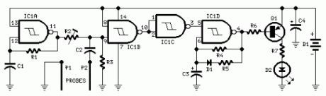
This plant watering monitor circuit is intended to signal when a plant needs water. A LED flashes at a low rate when the ground in the flower-pot is too dry, turning off when the moisture level is increasing. Adjusting R2 will allow the user to adapt the sensitivity of the circuit for different grounds, pots and probe types. IC1A and related components R1 and C1 form a 2KHz square wave oscillator feeding one gate input of IC1B through the voltage divider R2/R3 made variable by adjusting the Trimmer R2. If the resistance across the probes is low (as when there is a sufficient quantity of water into the pot) C2 diverts the square wave to ground, IC1B is blocked and its output will go steady hight. IC1C inverts the high status to low, thus keeping IC1D blocked: the LED is off.
When the ground in the flower-pot is becoming too dry the resistance across the probes will increase and C2 will be no longer able to divert the square wave to ground. Therefore, IC1B output begins to transfer the 2kHz signal to IC1C which, in turn, passes it to the oscillator built around IC1D.No longer disabled by a low level on its input, the IC1D oscillator slowly pulses Q1 base low causing the LED to flash, signalling the necessity to water the plant.
The short low pulse driving the base of Q1 is actually a burst of 2kHz pulses and therefore the LED flickers about 2,000 times per second – appearing to the human eye as if the LED was steadily on for the entire duration of the pulse.Some notes on this plant watering monitoring system
A square wave is used to avoid problems of probes oxidization.
Probes are made with two pieces of bare, stiff lighting cable of 1mm diameter and should be about 60mm long.
The probes should be driven fully in the pot’s ground about 30 – 50mm apart. Please note that all parameters regarding probes material, dimensions and spacing are not critical.
Current consumption: LED off = 150μA; LED on = 3mA for 0.1 sec. every about 2 sec. allowing the battery to last for years.
The quiescent current consumption is so low that the use of a power on/off switch was considered unnecessary. In any case, to switch the circuit completely off, you can short the probes.
Plant Watering Monitor circuit diagram
Components ValuesR1,R4 – 470K 1/4W ResistorsR2 – 47K 1/2W Trimmer Cermet or CarbonR3 – 100K 1/4W ResistorR5 – 3K3 1/4W ResistorR6 – 15K 1/4W ResistorR7 – 100R 1/4W Resistor
C1 – 1nF 63V Polyester CapacitorC2 – 330nF 63V Polyester CapacitorC3,C4 – 10μF 25V Electrolytic Capacitors
D1 – 1N4148 75V 150mA DiodeD2 – 5mm. Red LED
IC1 – 4093 Quad 2 input Schmitt NAND Gate IC
Q1 – BC557 45V 100mA PNP Transistor
P1,P2 – Probes (See Notes)
B1 – 3V Battery (2xAA, N or AAA 1.5V Cells in series) (View)
View full Circuit Diagram | Comments | Reading(902)
Homemade PCB
Published:2012/9/27 21:32:00 Author:muriel | Keyword: Homemade, PCB
Printed circuit board or PCB is one of the important things to assemble an electronic circuit. It provides support to the components and makes electrical connection between the parts. In PCB assembling, the components are placed on one side of the Copper laminate passing their pins or leads to the other side through the holes. The pins/leads are then soldered to connect with the PCB tracks. Here explains the easiest method to make a homemade PCB for prototyping.To make the PCB, following materials are required
1. Copper clad boardThis is available in different sizes. Select a suitable size to accommodate all the components. If the copper clad board is large in size, cut it to the required size using a Hacksaw blade. The copper clad board has a copper coated side which forms the soldering side. The other side is the component side on which the components are placed.If there is any dirt or copper oxide on the copper side, clean it throughly using a pencil eraser
Copper clad board
2. Ferric chloride solutionThis is the Etching solution of Ferric chloride. It removes the unwanted copper layers from the copper clad board. The Etching solution can be prepared by dissolving 50 gms Ferric chloride powder in 100 ml Luke warm water.
3. PCB drill and bits
PCB drill is used to drill holes in the PCB. A hand drill with suitable bits is sufficient for the purpose. Use drill bits of the following size to make holes for different components
A. 1mm – for IC pinsB. 1.2mm – for Resistor, capacitor, transistor etc.C. 1.5mm – for diode, LED pins, presets etc.D. 5mm – for LED, nuts, screws etc.E. 8mm – for switches, pots etc.
4. OHP Permanent Marker Pen, Tracing / Butter paper, Pencil Carbon paper, Varnish etc.
PCB Making
PCB making involves the following stages1. Draw the circuit diagram as compact as possible on a paper. Mark the points (component pins) to be drilled. This diagram is used for Pattern drawing on the copper clad board.
2. Draw the same diagram in the tracing / butter paper using the OHP marker pen. Draw the diagram carefully without any overlapping or shorting of tracks or components. The neatness of the PCB lies in the Pattern drawing. After drawing, see the other side of the paper. There is a Mirror Sketch of the tracks. This is the actual pattern of the PCB.
Mirror Sketch of PCB tracks
3. Place the Pencil carbon on the copper side of the copper clad board. The ink side of the carbon paper should face the copper layer.
4. Place the tracing paper with diagram over the carbon paper. The diagram should be in the middle part of the copper clad board. Fold the sides of the tracing and carbon papers and stick it using cello tape. This prevents the movement while drawing.
5. Once again redraw the diagram using the OHP marker pen so that the carbon ink will create a mirror sketch on the copper clad board.
6. Remove the tracing paper and carbon paper. Using the OHP marker pen, redraw the carbon pattern of the mirror sketch on the copper laminate. So that the tracks will be created using the permanent marker ink. Keep it for 10 minutes to dry the ink.
7. Mark points to be drilled. (View)
View full Circuit Diagram | Comments | Reading(1037)
Sync Signal Separator
Published:2012/9/27 21:31:00 Author:muriel | Keyword: Sync Signal, Separator

This simple sync signal separator circuit separates the composite sync signal into 2 separate horizontal and vertical sync signals.The composite signal can be directly used to drive the monitor’s horizontal sync input. That is why the composite signal line is connected directly to the H-sync line. To get the vertical sync signal, the double monoflop 74LS123 is needed as shown in the circuit diagram. The first monoflop time is somewhat longer than the distance between two line scan pulses. All horizontal line sync pulses are supressed. The second monoflop delivers only vertical sync pulses.
Sync Signal Separator circuit digram
(View)
View full Circuit Diagram | Comments | Reading(2432)
Automatic parking light switch circuit
Published:2012/9/27 21:30:00 Author:muriel | Keyword: Automatic, parking light, switch
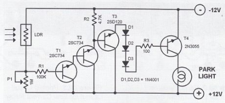
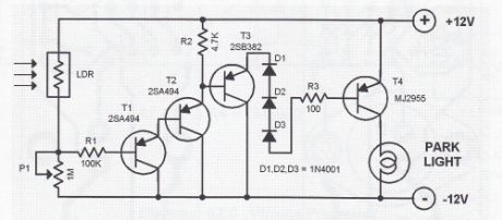
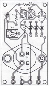
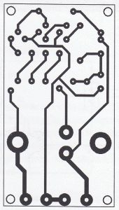
This automatic park light switch with LDR automatically turn ON the light when the surrounding light dims to a preset level. The first circuit diagram is an NPN design intended for negative grounded chassis. The second diagram is the PNP version intended for a positive grounded chasis.The dim level at which the circuit activates is set through the potentiometer P1.The printed circuit board layout can be used for both the negative and positive polarity chassis. Take note that the transistors and different for each chassis type. The connectors labeled in the parts placement diagram have the following connections:P = Power live of the carC = Car chassisB = Park light bulb
Automatic Park Light Switch Positive Ground
Automatic Park Light Switch Negative Ground
Parts Placement
Printed Circuit Board Layout
(View)
View full Circuit Diagram | Comments | Reading(1841)
Refrigerator Alarm Circuit
Published:2012/9/27 21:29:00 Author:muriel | Keyword: Refrigerator, Alarm Circuit
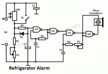
Use this refrigerator alarm circuit to prevent leaving the fridge door open by sending out an alarm signal every time the door is left open for some time.The sensor of the alarm is an LDR. After a short delay, it triggers an alarm signal and keep the signal on until the door is shut close.When the light falls on the LDR, it becomes low ohmic. The voltage at the junction of LDR/R2 charges the C2 via the R1 slowly. After about 10 seconds, the capacitor voltage reaches the input threshold of U1. Then U1 generates a square wave signal with a frequency of several Hertz. The time delay can be shortened by decreasing the value of R1 down to 220KΩ. U2 inverts the signal from U1. This inverted signal switches the U3 tone oscillator. When there is no light hitting the LDR, U3 is turned off. Finally, U4 amplifies the tone signal generated by U2 and drives the ceramic transducer. The frequency is doubled at the transducer.
The light sensitivity of the LDR can be adjusted with P1. The alarm tone freq. can be adjusted to the resonant freq. of the ceramic transducer through P2.
The maximum volume level can be reached when the tone freq. is equal to the ceramic transducer’s resonant freq..
The refrigerator alarm circuit can be powered with a small 9 volts battery. The current consumption is around 0.6 mA at standby and 5 mA when the alarm is activated.
Refrigerator Door Alarm circuit diagram
(View)
View full Circuit Diagram | Comments | Reading(2021)
Piezoelectric Heat Sensor
Published:2012/9/27 21:28:00 Author:muriel | Keyword: Piezoelectric, Heat, Sensor
Here is an Ultrasensitive Heat Sensor to monitor high temperature in Electronic devices. It can be placed inside the electronic gadget that usually generates heat during its operation. The circuit also functions as a sensitive Fire Alarm. This heat sensor uses the piezoelectric property to sense heat.
The sensor element is the ordinary piezo disc found in buzzer. The middle part of the piezo disc is coated with a layer of piezo electric material called Lead Zirconate. The crystals in this material are capable of dis-orientation and re-orientation when it is subjected to mechanical, electrical and heat stress. The Direct Piezo electric property of the piezoelectric crystals is the ability to generate electric signals when the crystals dis-orient and re-orient following a stress. This property is used here to sense temperature.
Piezoelectric Heat Sensor Circuit
A high gain type OP-Amp is used to sense the electrical signals from the piezo disc. The inverting (pin2) and non – inverting (pin3) inputs of the Op-Amp IC CA3140 are shorted through the capacitor C1, so that both the inputs will be in a balanced state. When this happens, output of IC1 remains low. When the piezo disc is subjected to heat stress, it generates a very small current that is enough for upsetting the balance of the inputs of IC1. This changes the output of IC1 from low to high. This high output is used to activate the alarm circuit based on the ROM IC UM3561.
Piezo Disc (View)
View full Circuit Diagram | Comments | Reading(1592)
PWM Inverter
Published:2012/9/27 21:28:00 Author:muriel | Keyword: PWM Inverter
Pulse Width Modulation or PWM technology is used in Inverters to give a steady output voltage of 230 or 110 V AC irrespective of the load. The Inverters based on the PWM technology are more superior to the conventional inverters. The use of MOSFETs in the output stage and the PWM technology makes these inverters ideal for all types of loads. In addition to the pulse width modulation, the PWM Inverters have additional circuits for protection and voltage control.The quality of the output wave form (230 / 110 volt AC) from the inverter determines its efficiency. The quality of the inverter output wave form is expressed using Fourier analysis data to calculate the ‘Total Harmonic Distortion’ (THD). THD is the square root of the sum of the squares of the harmonic voltage divided by the fundamental voltage.
THD = √ V2 2 + V3 2 + V4 2…………. Vn 2 / V1Based on the output waveforms, there are three types of Inverters. These are Sine wave, Modified Sine wave or Quasi sine wave and Square wave inverters.
Sine waveAlternating current has continuously varying voltage, which swings from positive to negative. This has an advantage in power transmission over long distance. Power from the Grid is carefully regulated to get a pure sine wave and also the sine wave radiate the least amount of radio power during long distance transmission. But it is expensive to generate sine wave in an inverter. Its quality is excellent and almost all electrical and electronic appliances work well in sine wave inverter.
Sine Wave
The sine wave is the AC waveform we get from the domestic lines and from the generator. The major advantage of sine wave inverter is that all of the house hold appliances are designed to operate in sine wave AC. Another advantage is that the sine wave is a form of soft temporal rise voltage and it lacks harmonic oscillations which can cause unwanted counter forces on engines, interference on radio equipments and surge current on condensers.
Modified Sine wave or Quasi Sine wave
Modified sine wave is designed to simulate a sine wave since the generation of sine wave is expensive. This waveform consists of a Flat Plateau of positive voltage, dropping abruptly to zero for a short period, then dropping again to a flat plateau of negative voltage. It then go back to zero again and returning to positive. This short pause at zero volts gives more power to 50 Hz fundamental frequency of AC than the simple square wave.
(View)
View full Circuit Diagram | Comments | Reading(1217)
Best of FM Transmitter circuits
Published:2012/9/27 21:25:00 Author:muriel | Keyword: FM Transmitter
Here are some DIY FM Transmitter circuits that we have been published on electroschematics.com. This do-it-yourself fm transmitters are pretty easy to build and will give you a good feeling when you’ll hear the music on the radio receiver.Don’t forget to write your comments and post some links if you know good designs that are not in the best of list.
Best of Do-it-yourself FM Transmitters
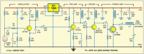
1W FM Transmitter with 4 transistors
This FM transmitter circuit uses four radio frequency stages: a VHF oscillator built around transistor BF494 (T1), a preamplifier built around transistor BF200 (T2), a driver built around transistor 2N2219 (T3) and a power amplifier built around transistor 2N3866 (T4).
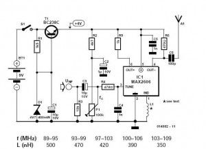
FM transmitter with MAX2606
Maxim now has available a series of five integrated oscillator building blocks in the MAX260x series which cover the frequency range between 45 and 650 MHz. The MAX2606 covers the VHF band, although the frequency can only be varied by approximately ±3 MHz around the midrange frequency set by the coil L.
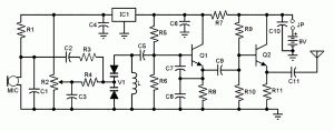
SMD FM Transmitter
Let’s construct a low-power FM transmitter using surface-mount devices (SMD) that will be received with a standard FM radio. Soldering surface mounted devices is not so hard and actually is quite easy. The figure below shows the schematic of the transmitter which consists of two stages: an oscillator and an output amplifier. Modulation is from an electret microphone but you can use a low power audio source.
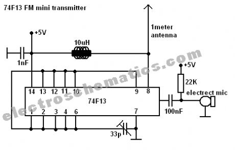
FM Bug Transmitter
Take a look at this fm spy transmitter which can be used as a bug transmitter or as fm bug too. It uses a single IC 74F13, one coil, a capacitor, one trimmer, one resistor and ofcourse one electret mic. This spy bug is so easy to build and can give you a total coverage range of about 3 to 5 meters. You may want to use a small 100mW amplifier to give a little extend transmission range so you can spy from other location.
(View)
View full Circuit Diagram | Comments | Reading(4474)
Bike Guard Alarm Circuit
Published:2012/9/27 21:25:00 Author:muriel | Keyword: Bike Guard, Alarm Circuit
This Simple circuit can be used to Guard your bike from theft. It gives a loud alarm tone if somebody tries to start the bike. The alarm disables only when the hide switch S2 is opened. The circuit has little component count and can be easily fixed in the bike.Working of the circuit is simple. The alarm generator buzzer or Horn is activated by an SCR and its triggering is under the control of the transistor T1. In the Armed position, Switch S2 is closed and S1 (Key switch of the bike) is opened. In this state, T1 will not conduct and SCR and Buzzer remains idle in armed position. When somebody turns on the Key switch of the Bike using a duplicate key, Capacitor C1 charges through R1, D1 and R2. It will take a time delay of few minutes to attain full charge in C1. When C1 fully charges T1 conducts and triggers the SCR. Buzzer connected to the Anode of SCR gets electrical path and it sounds the alarm. LED also lights to indicate the theft. The time delay is added through C1 so that the alarm will sound only after the bike is started .This aborts the attempt of theft.
Bike Guard Alarm Circuit diagram
The unit should hide in a place like the Carrier Box. So that switch S2 can be protected. An additional bike horn can be connected in the place of the buzzer to get loud sound. Connection point from R1 should go to the key switch point that goes to the engine so that; the unit will be activated only if the key switch is closed. Time delay can be changed by changing the value of C1 or R2. Hide switch S2 should be kept closed for arming the bike only after removing the switch key. Power to the circuit is obtained from the 6/12 volt bike battery. High current type transistor T1 and SCR are used to handle the high power of bike battery.Use 1 watt resistors to handle high power.Note: This circuit is not sufficient if the tricky thief knows some electronics. (View)
View full Circuit Diagram | Comments | Reading(1342)
Audio Noise Filter circuit
Published:2012/9/27 21:24:00 Author:muriel | Keyword: Audio, Noise Filter
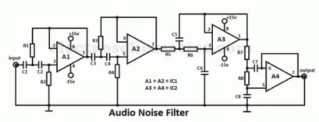
This audio noise filter circuit is a bandpass filter for audio frequency band. It filters unwanted signals that are lower or higher than the audio frequencies.It has 2 filters: a low pass filter and a high pass filter in a cascade configuration.Both filters are second-order filters with a 24 dB/octave fiter capability. The 3 dB cut-off freq. are 11.8 Hz and 10.7 kHz. The bandpass characteristic can be changed by changing the values of the capacitors and resistors. If you want to raise the bottom cut-off freq., you must reduce the values of C1 up to C4. For lowering the bottom cut-off freq. you must increase the values.
If you want to reduce the top cut-off f you must raise the values of R5 up to R8 and decrease it in order to increase the top cut-off frequency.
Noise Filter circuit diagram
Audio Noise Filter Parts ListR1 = R2 = 56kΩR3 = 39kΩR4 = 100kΩR5 = R6 = R7 = R8 = 3.3kΩC1 = C2 = C3 = C4 = 0.33µF ceramicC5 = C6 = 0.0033µF ceramicC7 = 0.0047µF ceramicC8 = 0.0018µF ceramicIC1 = IC2 = NE5532N (View)
View full Circuit Diagram | Comments | Reading(3982)
APR 9301 Voice Recorder
Published:2012/9/27 21:24:00 Author:muriel | Keyword: APR 9301, Voice Recorder
APR 9301 is a single chip Voice recorder and Play back device for 20 to 30 seconds voice recording and play back. It is an ideal IC for automatic answering machine, door phones etc. This IC has data storage capacity and requires no software and microcontroller. It provides high quality voice recording and play back up to 30 seconds.APR9301 Datasheet
The IC requires minimum components to create a voice recorder. The IC has non volatile flash memory technology with 100K recording cycles and 100 year message retention capacity. The IC utilizes the Invox proprietary analog / multi level flash non volatile memory cells that can store more than 256 voltage levels. It requires a single 5 volt supply and operates in 25 mA current.
APR 9301 Voice Recorder Circuit
Mode of operation
1. Record ModeThe LED glows when the IC records the voice obtained through the Mic. A single voice message up to 20 seconds can be recorded. The IC remains in the recorded mode as long as the RecL pin 27 is grounded. Recoding will be terminated with the last memory when 20 seconds is over. The Speaker driver will automatically mutes in the recording mode. By changing the value of the OscR resistor R1 it is possible to increase the recording period as follows
A. R1 52K 20 Sec.B. R1 67 K 24 SecC. R1 89 K 30 Sec.
APR 9301 IC
(View)
View full Circuit Diagram | Comments | Reading(1471)
CD Burner – How the CD Burning is done
Published:2012/9/27 21:23:00 Author:muriel | Keyword: CD Burner
CD burning is an amazing technology and its working principle is really fascinating. CD burners encode music and other datas on to the blank CD which can be retrieved through CD reading. CD stores the datas in digital form represented by a series of 1s and 0s. The 1s are represented by tiny bumps and the 0s as flat areas. Such millions of bumps and flats areas are present in a standard size CD.
A CD is made from 1.2 mm thick, almost-pure Polycarbonate plastic and weighs 15–20 grams. From the center outward components are at the center (spindle) hole, the first-transition area (clamping ring), the clamping area (stacking ring), the second-transition area (mirror band), the information (data) area, and the rim.
A CD is made up of a polycarbonate plastic known as Polymethyle Meta acrylic.The surface of the CD is coated with a thin layer of Aluminium to make it reflective, and is protected by a film of lacquer that is normally spin coated directly on top of the reflective layer, upon which the label print is applied.
The bumps and flat areas are present on the reflective side of the CD which is arranged in continuous tracks. These tracks measures about 0.5 microns and can stretch about 5 Kms. During CD reading, a ‘Read laser beam’ passes over the flat area in the track. The laser beam will reflect back which will be passed onto a photo sensor assembly. The Photo sensor interprets the reflected laser light as 1. When the laser light bounce back from the bumps, the photo sensor will not get it and the CD player recognize it as 0.
Blank CD
The bumps are arranged spirally starting from the centre of the CD to the periphery. The motor in CD player spins the CD in a steady speed. The laser assembly of the CD player moves from the center to the periphery of the CD at a steady speed to retrieve the data. The CD player shows a slow spinning speed as the laser assembly move outwards to keep the bumps moving past the laser at a constant rate. The digital information retrieved by the photo sensor will be then converted into audio or video by the amplifier circuit.
CD burring technique
CD writer is used to burn the CD to record the data in the digital format. The CD burner darkens microscopic areas in the reflective side of the ‘Blank CD’. During burning, both reflective and non reflective areas are created in the CD that can be interpreted as 1 and 0 by the CD player. The CD burner has a laser assembly similar to the CD reader. But the laser is ‘Write Laser’ with high power around 40 mW. The write laser interacts with the CD and alters its surface.
(View)
View full Circuit Diagram | Comments | Reading(1451)
Anti-theft Car Alarm circuit
Published:2012/9/27 21:23:00 Author:muriel | Keyword: Anti-theft, Car Alarm
Here is a simple Anti theft car alarm device for your Car. It generates a loud alarm when there is an attempt of theft. When the intruder opens the door, the circuit senses the attempt of theft and after 2 minutes, the alarm will be activated. The time delay is provided to help the user to leave the car after arming with the deviceThe anti theft alarm circuit taps power supply from the car battery. Switch S1 is the on/ off switch of the alarm circuit. When the circuit is activated through S1, the flashing LED blinks indicating that the car is armed. But the alarm generator works only if the Dome lamp of the car is switched on through the door switch. This switch turns on the dome lamp, if any one of the door is opened. The user can put S1 in the on position before leaving the car.
There will be a delay of 2 minutes so that the alarm will not be generated. When the intruder opens the door, Diode D1 forward biases and capacitor C1 charges through R1. It takes around 1 minute to charge C1. When C1 fully charges, the 12 volt Zener conducts to trigger the NPN transistor T1.Zener diode switch is provided to avoid false triggering and T1 conducts only when C1 charges fully. When T1 conducts C2 charges and the voltage in C2 triggers the gate of SCR. The Horn connected to the Anode of the SCR sounds indicating the theft. The horn can be either a spare car horn or a Hooter that gives loud alarm.
Anti-theft Car Alarm Circuit diagram
Note: Before leaving the car, switch on S1 and after entering the car switch off S1. Hide S1 in a place that cannot be detected. (View)
View full Circuit Diagram | Comments | Reading(1250)
IC CA3140 datasheet
Published:2012/9/27 21:22:00 Author:muriel | Keyword: CA3140
CA3140 is the 4.5MHz BiMOS Operational Amplifier with MOSFET inputs and Bipolar output. This Op Amp combines the advantage of PMOS transistors and high voltage bipolar transistors.
CA3140 has gate protected MOSFETs (PMOS) transistors in the input circuit to provide very high input impedance typically around 1.5T Ohms.The IC requires very low input current as low as 10pA to change the output status, high or low. The IC has very fast response and high speed of performance. The output stage of the IC uses bipolar transistors and includes built in protection against damage from load terminal short circuiting to either supply rails or to ground.
The use of PMOS FET in the input stage results in common mode input voltage capabilities down to 0.5 volts below the negative supply terminals. These operational amplifiers are internally phase compensated to achieve stable operation in unity gain follower operation, and additionally, have access terminal for a supplementary external capacitor if additional frequency roll-off is desired. Terminals are also provided for use in applications requiring input offset voltage Nulling.
Pin connectionsThe CA3140 Series has the same 8-lead pin out
Pin1Offset NullPin2 Inverting input INVPin3 Non inverting input Non-INVPin4 Ground- Negative supplyPin5 Offset NullPin6 OutputPin7 Positive supplyPin8 Strobe
Operating conditions
Supply voltage 36 volt maximumInput terminal current 1mA
CA3140 Block Diagram
Nulling of Offset Voltage
The input offset voltage can be nulled by connecting a 10K pot between the terminals 1 and 5 and returning its wiper to the ground. This technique, however, gives more adjustment range than required and therefore, a considerable portion of the potentiometer rotation is not fully utilized. (View)
View full Circuit Diagram | Comments | Reading(1593)
DIY LDR Switch Circuits
Published:2012/9/27 21:22:00 Author:muriel | Keyword: LDR Switch

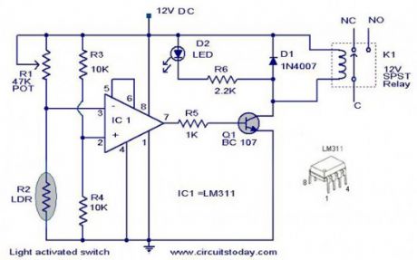
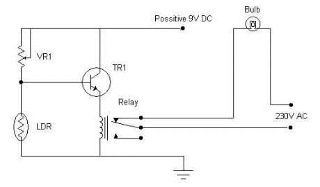
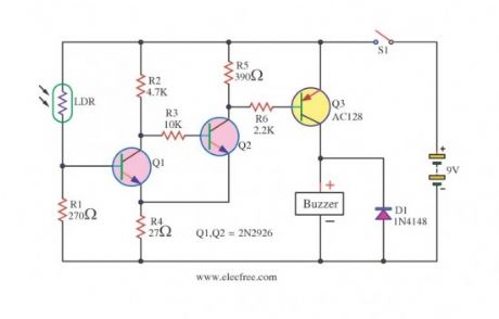
Here are some DIY LDR switch circuits available on our website and the web. LDR switches are used to switch a relay or other device when light are present or absent. LDRs or Light Dependent Resistors are very useful especially in light/dark sensor circuits.
Normally the resistance of an LDR is very high, sometimes as high as 1000 000 ohms, but when they are illuminated with light resistance drops dramatically.
LDR switch circuit diagrams
This is a light switch or light activated relay circuit. The relay on when LDR uncoverd and relay off when LDR covered. Adjust VR1 for light sensitive. LED will turn on at the same time with relay.Source: http://www.coolcircuit.com/circuit/light_switch/
This is the circuit diagram of a light activated switch based on National Semiconductors comparator IC LM 311 and a LDR.Source: http://www.circuitstoday.com/light-activated-switch-circuit
Light sensitive switch with LDR, actually it has a buzzer which will sound an alarm…Source: http://www.eleccircuit.com/light-sensitive-switch-with-ldr-2n2926/
(View)
View full Circuit Diagram | Comments | Reading(3701)
6v to 12v converter circuits
Published:2012/9/27 21:19:00 Author:muriel | Keyword: 6v to 12v, converter
Here are some of 6v to 12v converter circuits that can be used to convert a small voltage of about 6 volts to a higher voltage of 12 volts but ofcourse with a lower current rating.
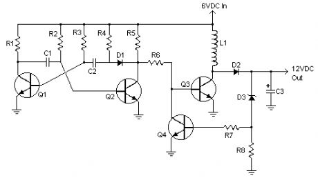
6 volts to 12 volts converters
This inverter circuit can provide up to 800mA of 12V power from a 6V supply. For example, you could run 12V car accessories in a 6V car. The circuit is simple, about 75% efficient and quite useful. By changing just a few components, you can also modify it for different voltages.
Source: http://www.aaroncake.net/circuits/6-12conv.asp
Parts List:R1, R4 - 2.2K 1/4W ResistorR2, R3 - 4.7K 1/4W ResistorR5 - 1K 1/4W ResistorR6 - 1.5K 1/4W ResistorR7 - 33K 1/4W ResistorR8 - 10K 1/4W ResistorC1,C2 - 0.1uF Ceramic Disc CapacitorC3 - 470uF 25V Electrolytic CapcitorD1 - 1N914 DiodeD2 - 1N4004 DiodeD3 - 12V 400mW Zener DiodeQ1, Q2, Q4 - BC547 NPN TransistorQ3 - BD679 NPN TransistorL1 - See Notes on the websiteMISC - Heatsink For Q3, Binding Posts (For Input/Output), Wire, Board
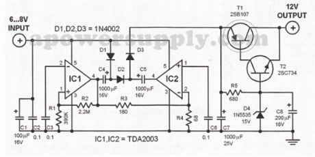
This 6V to 12V converter circuit is made with an IC from SGS with several additional components. The IC is a TDA2003 but it can be replaced with a TDA2002.The cost of building the 6volts to 12 volts converter should be low enough to justify constructing it instead of modifying the entire equipment setup to work directly with a 6 volts power supply. The two principles of simplicity and functions properly without the need of the transformer.
Source: http://apowersupply.com/6v-to-12v-converter-tda2003-144.html
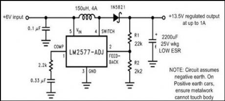
This is a Simple Switcher step-up voltage regulator made by National Semiconductor, (part number LM2577-ADJ). Together with a few extra components, a heat sink and some wiring, it is possible to generate over 1A from the battery of an Austin. The output connector is taken from a car charger extension lead, so that a phone or a sat-nav just plugs straight in.Source: http://www.austin7.org/6v_to_12v_converter.htm (View)
View full Circuit Diagram | Comments | Reading(3108)
Electronic Siren Circuit
Published:2012/9/27 21:19:00 Author:muriel | Keyword: Electronic Siren
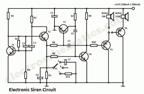
The DIY Electronic Siren circuit described here can create three different US-style siren sounds: DIY police, DIY ambulance and fire engine. The desired sound can be selected using switch S1. The circuit can be used in toys (such as model vehicles), as part of an alarm system, and in many other applications. For use in a toy, a BC337 is an adequate device for driver T5, since it is capable of directly driving a 200mW (8?) loudspeaker. In this case the current consumption from a 9 V power supply is around 140 mA. If a louder sound is required, a BD136 is recommended: this can drive a 5W (8?) loudspeaker. This will be the sound produced with the switch S1 on this positions:
a: Fire Brigade Siren
b: Police Siren
c: Ambulance Siren
The current consumption of the electronic siren from a 12 V supply will then be about 180mA. If still more volume is desired, then T5 (a BD136) can be used as a first driver stage, and a 15W (8?) loudspeaker can be connected via output transistor T6. Here an AD162 or an MJ2955 can be used, which, for continuous operation, must be provided with cooling. The peak current consumption of the circuit will now be about 500mA with a 12V power supply. Capacitor C1 is not required for battery operation.
Sent by Mihai Dorin, Romania. Thanks!
DIY Electronic Siren Circuit Diagram
Parts ListR1 = R9 = 2.2KΩR2 = 470ΩR3 = 47KΩR4 = R8 = 22KΩR5 = R6 = R7 = 18KΩR10 = 3.3KΩC1 = 100µF/16VC2 = 2.2µF/16VC3 = 10µF/16VC4 = 47µF/16VC5 = 22nFC6 = 33nFC7 = 470µF/16VT1 = T2 = T3 = T4 = BC547T5 = see textT6 = MJ2955, AD162
(View)
View full Circuit Diagram | Comments | Reading(2186)
The reducing and cut-off frequency circuit with capacitor( wideband strain signal conditioner 1B31)
Published:2012/9/26 22:29:00 Author:Ecco | Keyword: reducing , cut-off frequency , capacitor, wideband , strain signal , conditioner
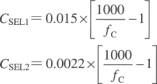
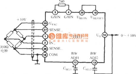
The external capacitors CSEL1 and CSEL2 can set cutoff frequency of low pass filter below 1kHz to meet the needs of the application of narrowband, and the circuit is shown in Figure. The capacitance is calculated as following:
(View)
View full Circuit Diagram | Comments | Reading(1042)
The excitation voltage enhancing circuit ( broadband strain signal conditioner 1B31 )
Published:2012/9/26 21:22:00 Author:Ecco | Keyword: excitation voltage , enhancing circuit, broadband strain , signal conditioner


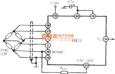
When broadband strain signal conditioner 1B31's pin 19 connects to pin 20, the excitation voltage output by programmable bridge excitation source UEXC = +10 V. In order to upgrade UEXC to +10 ~ +15 V, it must be connected to a resistor REXT between the XC ADJ end and SENSE- end, the circuit is shown in the figure. REXT value is determined by the following formula ( resistance units kΩ):
(View)
View full Circuit Diagram | Comments | Reading(951)
| Pages:316/2234 At 20301302303304305306307308309310311312313314315316317318319320Under 20 |
Circuit Categories
power supply circuit
Amplifier Circuit
Basic Circuit
LED and Light Circuit
Sensor Circuit
Signal Processing
Electrical Equipment Circuit
Control Circuit
Remote Control Circuit
A/D-D/A Converter Circuit
Audio Circuit
Measuring and Test Circuit
Communication Circuit
Computer-Related Circuit
555 Circuit
Automotive Circuit
Repairing Circuit