
Circuit Diagram
Index 310
VMOS 144 MHz Push Pull DV28120T amplifier
Published:2012/10/9 2:41:00 Author:muriel | Keyword: 144 MHz, Push Pull, DV28120T, amplifier
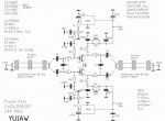
This is a 2 meters 144 Mhz rf amplifier wich works in push pull and is build with DV28120T Vmos.You can use coils made form RG142 coaxial cable or similar, 620mm long , 5mm diameter, 6 turns with inside diameter 30mm no gaps between.
VMOS RF amplifier circuit diagram
(View)
View full Circuit Diagram | Comments | Reading(1414)
Static Charge Monitor
Published:2012/10/9 2:41:00 Author:muriel | Keyword: Static Charge, Monitor
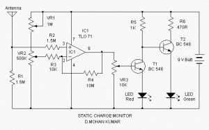
Here is a circuit that can sense the static electricity level in the atmosphere. It gives LED indications for both positive and negative atmosphere charges. The circuit uses a low noise JFET input Opamp TLO 71 to detect the atmospheric charge.The op amp has well matched high voltage JFET input device for low input offset voltage. The BIFET technology provides wide bandwidth and fast slew rate with two input bias currents. IC1 (TLO71) is designed as a voltage sensor cum signal amplifier. Its Non INV input is connected to the aerial (1 meter plastic wire) through R2. R1 maintains the input impedance of IC1 to make the input sensitivity normal.
VR1 and VR2 adjust the voltage level at the INV input of IC1. Resistor R3 and R4 determines the gain of the inverting amplifier and with the shown values it is 1000. That is, a difference of 1 milli volt at the input gives 1 volt output. Output from IC1 is used to switch on T1 and T2 at different output states.
When there is positive charge in the atmosphere, output of IC1 becomes high and T1 conducts to light Red LED. If the atmospheric charge is negative, output of IC1 remains low and T1 off. This causes T2 to conduct and Green LED lights. These states of LEDs change as the atmospheric charge changes. Adjust VR1 and VR2 for IC’s input sensitivity and VR3 for the threshold level of T1.Adjustments should be done in a sunny day so that atmospheric charge will be around 100 milli volts.
Static Charge Monitor Circuit Diagram
(View)
View full Circuit Diagram | Comments | Reading(1379)
DC Voltage Doubler Circuit with 555
Published:2012/10/9 2:40:00 Author:muriel | Keyword: DC Voltage, Doubler, 555
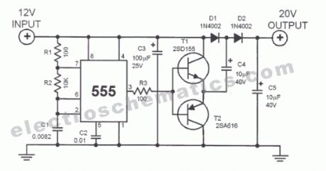
This dc voltage doubler circuit produces a voltage that is twice its voltage supply. This is useful when a higher voltage level is needed out of a single lower voltage power supply. Since the current consumption levels are low in such cases, the circuit can be built with minimal resources.
Voltage Doubler Circuit Schematic
The electronic circuit is basically a square wave generator using the common LM555 timer IC. It is followed by a final stage made of transistors T1 and T2. The actual doubler circuit is made of D1, D2, C4 and C5 components.
The 555 dc voltage doubler timer IC works as an astable multivibrator and generates a frequency of about 8.5 kHz. The quare wave output drives the final stage made of T1 and T2. This is how the doubler works: by a low amplitude of the signal, transistor T1 blocks while T2 conducts. The minus electrode of the capacitor C4 is grounded and charges through D1. By a high amplitude of the signal, transistor T1 conducts while T2 blocks. However, capacitor C4 cannot discharge because it is blocked by D1. The following capacitor C5 is therefore charged with a combined voltage from C4 and the power supply (12V input).On standby, the circuit delivers around 20 volts The maximum load must not exceed 70 mA. The actual output voltage is around 18 volts giving an efficiency rating of 32 %. On lower current ratings, the voltage is higher. If a stable voltage lever is desired, a 3 pin voltage regulator IC can be added at the output. The regulator IC’s own current consumption must be added to the total current consumption which must not exceed 70 mA.For more voltage doublers check the related posts bellow.
(View)
View full Circuit Diagram | Comments | Reading(3030)
TSOP 1738 Photo module Design notes
Published:2012/10/9 2:40:00 Author:muriel | Keyword: Photo module
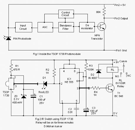
TSOP 17… Series Photomodules are excellent Infrared sensors for remote control applications. These IR sensors are designed for improved shielding against electrical field disturbances.TSOP 1738 Photo module Design notesTSOP 17…. Series Photomodules are miniature IR sensor modules with PIN photodiode and a preamplifier stage enclosed in an epoxy case. Its output is active low and gives +5 V when off. The demodulated output can be directly decoded by a microprocessor. The important features of the module includes internal filter for PCM frequency, TTL and CMOS compatibility, low power consumption (5 volt and 5 mA), immunity against ambient light, noise protection etc. The added features are continuous data transmission up to 2400 bps and suitable burst length of 10 cycles per burst.Inside the Photo moduleThe photo module has a circuitry inside for amplifying the coded pulses from the IR transmitter. The front end of the circuit has a PIN photodiode and the input signal is passed into an Automatic Gain Control(AGC) stage from which the signal passes into a Band pass filter and finally into a demodulator. The demodulated output drives an NPN transistor. The collector of this transistor forms the output at pin3 of the module. Output remains high giving + 5 V in the standby state and sinks current when the PIN photodiode receives the modulated IR signals. Block diagram is given in Fig 1
Pin assignment
Photomodules are 3 pin devices. These pins are assigned for +V,–V and output. The pin assignment of TSOP 17… series from the front side (projected side) is Pin 1 Ground, Pin 2 + 5V and pin 3 Output. The photo module requires regulated 5V supply. If the supply voltage increases, the device will be destroyed.
The pin assignment (Front view) of some common Photomodules
Type pins 1 2 3 Response frequencyTSOP 1730 G 5V OP 30 kHzTSOP 1736 G 5V OP 36 kHzTSOP 1738 G 5V OP 38 kHzTSOP 1756 G 5V OP 56 kHzTSOP 1236 G 5V OP 36.7 kHzTSOP 1838 OP G 5V 38 kHzTSOP 1138 G 5V OP 38 kHzTK 1836 OP G 5V 36 kHzSFH 506-38 G 5V OP 38 kHzRPM 7238F OP G 5V 37.9 kHz
Design considerations
For the proper functioning of the Photo module, it is necessary to consider some important aspects.1. Supply voltage should be + 5 Volts. For this, a 5.1 volt Zener must be connected to the +V pin and ground.2. A 100 uF capacitor should be connected to the +V pin as a buffer and filter capacitor. This will suppress the power supply disturbances.3. Carrier frequency should be close to the center frequency of the band pass filter. 38 kHz in the case of TSOP 1738.4. Burst length must be 10 cycles per burst or more.5. Between each 10 to 70 cycles, a gap time of 14 cycles is necessary to reset the module.6. DC lights such as tungsten bulb and daylight affects the functioning of the photo module.7. Signals from Fluorescent lamps with electronic ballast will affect the working of the photo module.8. Continuous IR signal (non- pulsed) will disturb the photo module and it will not responds to it.
Photo module design is given in Fig.2
(View)
View full Circuit Diagram | Comments | Reading(1813)
TDA2822 Stereo Amplifier Circuit
Published:2012/10/9 2:40:00 Author:muriel | Keyword: TDA2822, Stereo Amplifier
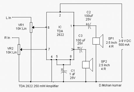
TDA2822 is a low power stereo Op Amp used in Walkman players and Hearing aids. It can give 250 milli watts output. TDA2822 is an ideal Op amp for low output applications. It is a good choice as a preamplifier in stereo high power amplifier circuits. It has two inputs and two outputs which can deliver 250 milli watts output power. The amplifier circuit with in the IC is well set for noise free operation. Outputs can be directly coupled to the speakers through the decoupling capacitors.
TDA2822 amplifier circuit diagram
(View)
View full Circuit Diagram | Comments | Reading(2596)
Power supply 4-30V 20A LM338
Published:2012/10/9 2:39:00 Author:muriel | Keyword: Power supply,4-30V, 20A, LM338
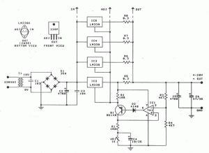
This is a regulated and adjustable power supply which can deliver up to 20A and adjustable voltage between 4 and 30V. It is easy to build and uses LM338 and 741 integrated circuits. VR1 it is used to adjust the output voltage.
LM338 power supply circuit schematic
(View)
View full Circuit Diagram | Comments | Reading(2873)
Logic State Indicator
Published:2012/10/9 2:39:00 Author:muriel | Keyword: Logic State, Indicator
Here is a simple logic state indicator to test whether the output of digital IC is in logic 1 or 0. The Bicolor LED lights Green when the logic state is 1 and lights Red when the logic state is 0.The circuit uses only a few components and is based on the switching action of bipolar transistor. Normally the base of T1 is floating so that it will be off. This will allow T2 to conducts since its base gets bias through R2. The Red half of the bicolor LED lights indicating 0 logic. When the red probe connected to the base of T1 makes contact with a high signal output, T1 conducts and Green half of bicolor LED lights indicating logic 1. At the same time, T2 turns off and Red half of bicolor LED turns off. If the output is pulsating with alternate cycles, Red and Green LEDs lights alternately and if the transition is very fast both Red and Green LEDs lights giving yellow colour. The circuit can also be used as a continuity tester or Fuse tester.
Logic Stage Indicator Circuit Diagram
(View)
View full Circuit Diagram | Comments | Reading(769)
Peak indicator circuit schematic TLC272
Published:2012/10/9 2:37:00 Author:muriel | Keyword: Peak indicator
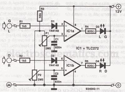
This peak indicator circuit signals thru 2 led’s the exceeding of a pre-estabilished value of any stereo audio channel.Signals from the 2 channels are rectified (monoalternance) with D1 and D2 and the resulted voltage is applied on OA IC TLC272 inversor entries.The peak indicator circuit can be used up to 20kHz frequency and the current consumption with led off is 0.25mA and with both leds on is 24mA.
Peak indicator circuit schematic
(View)
View full Circuit Diagram | Comments | Reading(1316)
LED Alarm Simulator circuit
Published:2012/10/9 2:37:00 Author:muriel | Keyword: LED Alarm, Simulator circuit
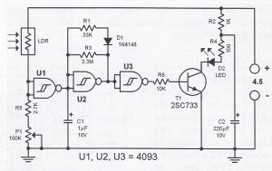
This circuit simulates an alarm to discourage thieves and it is originally designed to be used on bicycles but can be used for cars too. It blinks a LED on and off thus simulating a real alarm circuit.
The LED alarm electronic circuit consists of a square wave oscillator generating a 1 MHz signal with a pulse width of 10 milisecond. The LED lights u 10 miliseconds long. The circuit consumes 30 miliamperes when the LED lights and the average consumption is 300 microamperes.To switch off the circuit automatically it has a built in LDR. When the LDR is exposed to light it becomes low ohmic and the output of U1 becomes 0. The oscillator stops and the LED turns off. The light sensitivity of the circuit is set with the potentiometer P1.
When there is no light falling on the LDR, the input of U1 is connected to the ground and its output becomes “1″ thereby starting the oscillator which drives the LED to blink. If the circuit is powered with a 4.5 volts battery that has a 2 Ah capacity, it will work for aroung 1.5 years.
LED flashing alarm circuit diagram
(View)
View full Circuit Diagram | Comments | Reading(875)
Water Level Sensor Circuit
Published:2012/10/9 2:37:00 Author:muriel | Keyword: Water Level, Sensor
This simple water level sensor circuit monitors the presence of water in a certain location or container. The circuit sends an acoustic alarm when it senses a drop of water leak. It is very simple to build and it is made of a single IC and some passive components. Check out the water level indicator circuit too!The IC LM1801 is a low power comparator that can deliver high output current if needed. When water hits the sensor, the reference voltage is overshot and the IC drives the ceramic transducer to beep. It is also possible to connect several sensors to the water level monitor circuit. The sensor can be easibly made out of a small piece of PCB that is etched with the proper pattern. The decoupling capacitor C3 is a 100uF/16V electrolytic capacitor.
Water Level Sensor Circuit Diagram
Water Level Sensor PCB and Parts
(View)
View full Circuit Diagram | Comments | Reading(2953)
LED Optocoupler circuit
Published:2012/10/9 2:36:00 Author:muriel | Keyword: LED Optocoupler
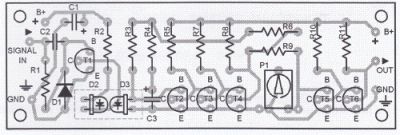
This LED Optocoupler circuit uses two ordinary LEDs as the optocoupler element. When a voltage of 2V is fed to the input, LED 2 will generate a voltage that is strong enough to switch on transistor T5. The upper frequency limit is around 38 kHz. Very low pulse frequencies are almost meaningless for the circuit.Eventhough the LEDs are quite intensive to stray light, it is a good idea to enclose them with an opaque box. Resistor R2 must be selected basing on the power supply voltage. It can be between 680 Ω and 1 KΩ. Resistor R11 must not be lower than 220 Ω.Transistor T6 has an open-collecter character.
Optocoupler Circuit Diagram
Optocoupler PCB and Parts Placement
(View)
View full Circuit Diagram | Comments | Reading(1441)
Water Level Indicator circuit
Published:2012/10/9 2:36:00 Author:muriel | Keyword: Water Level, Indicator
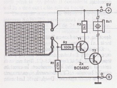
This simple water level indicator will activate a buzzer in order to make a noise when a certain level of water is being reached. Because the water sensor and the command circuit are located on the same printed circuit board, indicator, together with its 9 V battery and the buzzer can be mounted in a compact case. Obviously the sensor, that is made by corossion, on the board, must not be mounted directly on iron or steel bathtubs but with a magnet atached on the case. Check out the new water level sensor circuit.
Water Level Indicator Circuit Diagram
In order to avoid the scratching of the bathtub, the magnet can be covered with plastic or rubber. If the bathtub is made of polypropylene, the water indicator must be attached to it with two clamps or double adhesive tape.
When the water reaches the sensor T1 base is connected to the positive terminal. In consequence, T1 and T2 are opening and the buzzer it makes a buzz. The current consumption is now around 25 mA.
In order that the water level sensor circuit will not be put into operation by steam it may be necessary the reduction of the sensibility by increasing the value of R2. Is recommended to tin the PCB in order to avoid corossion.
Water Level Indicator PCB Layout
(View)
View full Circuit Diagram | Comments | Reading(2856)
Linear Optocoupler Circuit
Published:2012/10/9 2:35:00 Author:muriel | Keyword: Linear Optocoupler
This linear optocoupler is built with MOC5010 and can be used to isolate a circuit from main grid, audio interface, in medical electronics and many other applications. Because of its high isolation resistance (1011 Ω), MOC5010 is used in applications where a circuit is powered directly from main power. With a bandwidth from 5 Hz to 100 kHz you have no reason to complain about audio signal response.MOC5010 transforms an input current variation into an output voltage variation. The linear optocoupler circuit presented here has an amplification factor of 0.75. The input must not overcome 2 Vef while bandwidth is 118 kHz at -3 dB.Amplifier A has a transfer resistance of 200 mV/mA resulting in a total amplification of 0.6 … 0.8 (-4.5 … -2 dB). The output impedance is not higher than 200 Ω so you can connect an external amplifier at pin 4. If the input voltages are higher than 2 Vef then connect a potentiometer as voltage divider like showing below optocoupler circuit diagram.
Linear Optocoupler Circuit Diagram
If the global amplification is too small use a regular transistor instead of FET T1. It is important to mention that 2 separate power supplies are required: both the +12 V terminals as well the 0V (ground) must be isolated from one another. In many cases it is possible to use a 12V voltage for the transmitter part from the connected device. (View)
View full Circuit Diagram | Comments | Reading(1124)
Triangle Wave Generator circuit
Published:2012/10/9 2:35:00 Author:muriel | Keyword: Triangle, Wave Generator
This triangle wave generator is made with a trigger Schmitt that converts a triangle wave into a rectangular one used to charge and discharge a capacitor through current sources. The positive current source T1 provide the charging and T2 the discharging. The trigger Schmitt is made from OR-EXCL gates IC1a and IC1b.The rectangular signal amplitude must not be higher than the T1 and T2 base voltage. Assuming a 10 V power supply, results that the amplitude will be 2.5V. IC2 is a good quality operational amplifier (200 V/us) that acts like a buffer between Schmitt input and output.
The triangle wave generator circuit can generate signals with frequencies up to 300 kHz. With the component values presented in the diagram the output wave frequency is 38 kHz. The frequency can be adjusted by changing C1′s value. The wave generator assembly absorbs around 8 mA, of which 5 mA runs thru IC2.
Triangle Wave Generator Circuit Diagram
(View)
View full Circuit Diagram | Comments | Reading(1042)
Infrared Receiver circuit with BPW41N
Published:2012/10/9 2:35:00 Author:muriel | Keyword: Infrared Receiver circuit
This infrared receiver is used with this infrared transmitter. The output signal of D1 IR diode is amplified by IC1. The diode is BPW41N works great with the transmitter and is relatively fast (~200 ns). The impulses at IC1′s output are applied to IC2 (comparator) that separate them from ambient light. Check out the infrared alarm circuit too.The infrared received signal is decoded by a simple 2 divider, IC3a. Each impulse produces a change of the state at the stage output. The output signal is filtered with R7-C11 and decoupled with C12, resulting in an audio signal suitable for control of high impedance headphones.
Infrared Receiver Circuit Diagram
The output signal of the infrared receiver can be improved with the help of an order 3 active low-pass filter (cut freq at 10 – 12 kHz) that will serve as buffer stage too. With the receiver placed at 1 meter distance from the transmitter and 30% modulation, the signal to noise ratio is -50 dB. The maximum working distance without interferences was around 5 meters. The IR receiver circuit absorbs a current around 15 mA, this makes it advisable to use a rechargeable battery (NiCd). (View)
View full Circuit Diagram | Comments | Reading(827)
Impulse modulation infrared transmitter circuit
Published:2012/10/9 2:34:00 Author:muriel | Keyword: Impulse modulation, infrared transmitter
This infrared transmitter can be used with this infrared receiver. This transmitter uses. The modulated signal is produced by comparison of an audio signal with a triangle signal of high frequency using a comparator IC. An appropriate triangle signal generator must have the offset equal with half of the 5V power supply voltage and the triangular signal size is 2.5V. Check out the infrared alarm circuit too.For a wider range of the infrared transmitter the current through LEDs must he high. Because the LED cannot stand high dc currents, the impulses must be short so we use PWM. The pulses are generated by XOR gate IC2d that compares the original PWM signal with the delayed by R5-C3-IC2c. The IC2d output signal produce T1 switching and in this way the LEDs absorbed current is limited at 400 mA peak with help from R6. The average current consumption of the infrared transmitter circuit will be around 90 mA.
P3 adjustment is made without input signal with help of an oscilloscope, so that all impulses from the output signal have the same width. Then adjust P2 so that the intervals between impulses come equal. IC1 output will then be a perfect rectangular wave.
Working with the receiver and the transmitter at the same time feed an input signal at maximum value then adjust P1 to obtain minimum interference in the received signal. Finally, you may use IC2a and IC2b for the triangle signal generator.
Infrared Transmitter Circuit Diagram
(View)
View full Circuit Diagram | Comments | Reading(842)
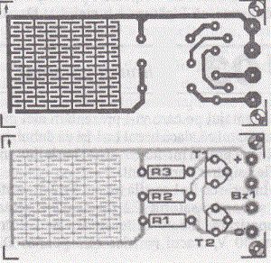
Solar Charger Circuit
Published:2012/10/9 2:32:00 Author:muriel | Keyword: Solar Charger
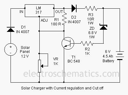
Here is a solar charger circuit that is used to charge Lead Acid or Ni-Cd batteries using the solar energy power. The circuit harvests solar energy to charge a 6 volt 4.5 Ah rechargeable battery for various applications. The charger has Voltage and Current regulation and Over voltage cut off facilities.
Solar Charger Circuit Diagram
The circuit uses a 12 volt solar panel and a variable voltage regulator IC LM 317. The solar panel consists of solar cells each rated at 1.2 volts. 12 volt DC is available from the panel to charge the battery. Charging current passes through D1 to the voltage regulator IC LM 317. By adjusting its Adjust pin, output voltage and current can be regulated.
VR is placed between the adjust pin and ground to provide an output voltage of 9 volts to the battery. Resistor R3 Restrict the charging current and diode D2 prevents discharge of current from the battery. Transistor T1 and Zener diode ZD act as a cut off switch when the battery is full. Normally T1 is off and battery gets charging current.
When the terminal voltage of the battery rises above 6.8 volts, Zener conducts and provides base current to T1. It then turns on grounding the output of LM 317 to stop charging. (View)
View full Circuit Diagram | Comments | Reading(5161)
Solar Charger Monitor circuit
Published:2012/10/9 2:31:00 Author:muriel | Keyword: Solar Charger, Monitor
This add on circuit can be attached to the solar charger to see whether the battery is charging or not. It lights a Red LED to indicate that the battery is not accepting charge. It gives a warning indication if there is any loose connection with the charger and battery.The Solar charger monitor circuit uses two PNP transistors T1 and T2 to give a warning indication if there is any loose connection with the charger and battery. If the connection is intact and current is flowing into the battery, diodes D2 and D3 forward bias and drops around 1.2 volts. This forward voltage drop across the diodes causes T2 to conducts. The collector current from T2 keeps the base of T1 high and it remains off. Red LED connected to the emitter of T1 remains off indicating that current is flowing to the battery and the connections are intact. When there is any break in the connecting cables or any loose contacts in the terminals, no more current passes and D2 and D3 reverse biases. This turns off T2 and T1 conducts .LED lights indicating that battery is not getting charging current.
Solar Charger Monitor Circuit Diagram
(View)
View full Circuit Diagram | Comments | Reading(925)
Temperature Controlled DC Fan
Published:2012/10/9 2:31:00 Author:muriel | Keyword: Temperature Controlled, DC Fan
This circuit can cool your heat generating electronic devices by operating a DC fan when the temperature in its vicinity increases above the preset level. Its operation is fully automatic and turns off when the temperature returns normal. It uses a small 12V DC brush less fan used in computersThe circuit exploits the property of Thermistor to operate the DC Fan. Thermistor is a kind of temperature dependent resistor and its resistance varies depending on the temperature in its vicinity. There are two types of Thermistors- NTC and PTC. Negative temperature coefficient (NTC) Thermistor decreases its resistance when the temperature increases while Positive temperature coefficient (PTC) increases its resistance when the temperature increases. Thermistors are bead like resistors available from 100 ohms to 10K or more values. Here a 4.7K NTC Thermistor is used. IC uA 741 is used as a voltage comparator to switch on the DC fan. Its INV input (pin2) gets an adjustable voltage through VR while its Non-INV (pin3) input gets voltage through a potential divider comprising R1 and the Thermistor. Thus the voltage at pin3 depends on the conductivity of the Thermister.
When the temperature is normal (as set by VR), pin3 gets higher voltage than pin2 and makes the output of IC high as indicated by Red LED. This high output keeps T1 off since its base is positive. DC fan remains off in this condition. When the temperature increases above the value set by VR, resistance of Thermister decreases and the voltage at pin3 decreases. As a result, output of IC becomes low to switch on T1. A small brush less DC fan (one used in computers) turns on to increase the air circulation. When the temperature returns normal, Fan automatically turns off. Diode D3 is necessary to remove back e.m.f when T1 turns off. Green LED indicates that the Fan is operating.
DC Fan Controlled by Temperature Circuit Diagram
(View)
View full Circuit Diagram | Comments | Reading(1470)
Voltage to Frequency Converter Circuit
Published:2012/10/9 2:31:00 Author:muriel | Keyword: Voltage,Frequency, Converter
This voltage to frequency converter circuit has an oscillator that is voltage controlled and has a small, 0.5% deviation. IC1 function as a multivibrator and produces rectangular impulses with equal width.The width of the impulses depend on R4, P1 and C1. With P1 we can do fine adjustments of the output frequency.
The output frequency can be easily adjusted with the help of U1 voltage. D3 diode is required because we want to eliminate R4 and P1 influence. D1 and D2 diodes produce a small flow of temperature. With P2 we adjust the offset voltage. Because of its high quality, this voltage-frequency converter (VCO) can be used in a large field of applications.
Voltage-Frequency Converter Circuit Diagram
(View)
View full Circuit Diagram | Comments | Reading(1072)
| Pages:310/2234 At 20301302303304305306307308309310311312313314315316317318319320Under 20 |
Circuit Categories
power supply circuit
Amplifier Circuit
Basic Circuit
LED and Light Circuit
Sensor Circuit
Signal Processing
Electrical Equipment Circuit
Control Circuit
Remote Control Circuit
A/D-D/A Converter Circuit
Audio Circuit
Measuring and Test Circuit
Communication Circuit
Computer-Related Circuit
555 Circuit
Automotive Circuit
Repairing Circuit