
Circuit Diagram
Index 309
25W FM radio amplifier circuit
Published:2012/10/10 1:51:00 Author:muriel | Keyword: 25W, FM, radio amplifier
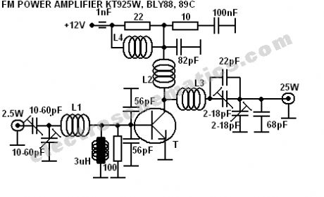
A simple 25W fm radio amplifier used as a final stage for a 2.5W transmitter. I has a total gain of 10 dB and needs a 12V / 3A power supply. It is equiped with KT925W or BLY88, BLY89C. Use a very good headsink because this transistor get very hot Coils values:L1 = L3 = 4 turns / 1.5mm / 8mm / 10mm longL2 = 4 turns / 1mm/6mm/10mm longL4 = 20 turns / 0.8mm / on 22Ω resistor
25W FM radio amplifier circuit schematic
(View)
View full Circuit Diagram | Comments | Reading(1605)
Dynamic compressor – passive components, no power supply
Published:2012/10/10 1:50:00 Author:muriel | Keyword: Dynamic compressor
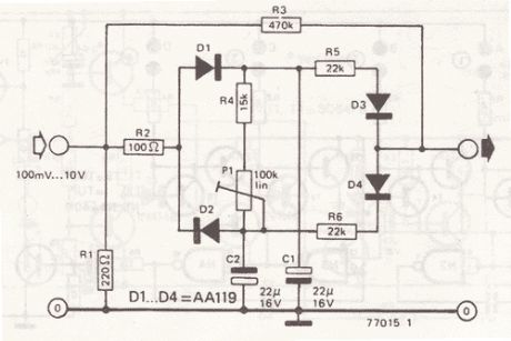
This dynamic compressor with passive components reduces high signal to a lower, more constant signal. If you look at this compressor schematic , you’ll notice it has no power supply, the required power is obtain thru the output signal.If you respect the schematic values this audio compressor will output a constant 70mV when the input voltage is between 100mV and 10V !
Passive compresor circuit diagram
(View)
View full Circuit Diagram | Comments | Reading(1584)
Metal Detector DIY Circuit
Published:2012/10/10 1:50:00 Author:muriel | Keyword: Metal Detector
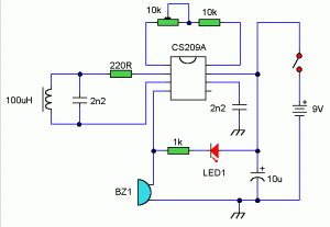
The heart of this diy metal detector circuit is CS209A. The metal detector it is build with one coil of 100uH. CS209A has one oscillator wich forms an LC circuit, the inductance of the coil will change when it is near metal objects.LED 1 will light and the buzzer turns on when the coil is changing inductance. The setup is easy, VR1 is adjusted ( away from any metal objects ) so that LED 1 will light and the buzzor sounds on, and then VR1 will be trimmed until led and buzzer are off.
DIY metal detector circuit
(View)
View full Circuit Diagram | Comments | Reading(2487)
Seismic Sensor circuit
Published:2012/10/10 1:50:00 Author:muriel | Keyword: Seismic Sensor
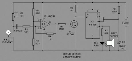
Here is an ultra sensitive vibration alarm that can sense very minute earth borne vibrations. It can be used to detect vibrations in the earth (Earth quake?). So it is an ideal device to monitor entry passages. The circuit exploits the direct piezo electric property of the piezo element used in buzzers.The Lead Zirconate crystals present in the piezoelement can readily store current and can release the current when the orientations of the crystals are disturbed through mechanical vibrations. IC1 amplifies the signals from the piezo element and the high output from IC1 switches on T1. When T1 conducts, trigger pin 2 of the monostable (IC2) will grounded to give 3 minutes high output.
This high output is used to sound alarm and to light LED. VR adjusts the sensitivity of piezo element. Glue the fine side of the piezo element on the floor (if used as an entry alarm) or inside a metal box (if used to bury in soil to detect earth borne vibrations).
Seismic Sensor Circuit Diagram
(View)
View full Circuit Diagram | Comments | Reading(3134)
Heat Sensor Circuit
Published:2012/10/10 1:49:00 Author:muriel | Keyword: Heat Sensor
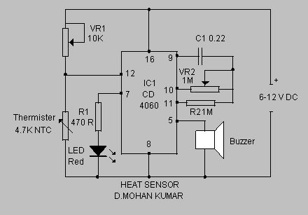
This simple circuit senses heat from electronic devices and gives warning alarm.It is an ideal add on circuit to monitor heat in CD players, Amplifiers etc.
(View)
View full Circuit Diagram | Comments | Reading(3318)
Stereo Pll fm transmitter BH1417
Published:2012/10/10 1:48:00 Author:muriel | Keyword: Stereo Pll, fm transmitter
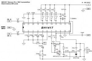
This BH1417 pll fm transmitter includes features like: pre-emphasis, sound limiter, stereo transmission, low pass filter, pll circuit, fm oscillator and rf output buffer. The sound limiter maintains the same audio level so no distorsions occur, the stereo encoder separates the left and right channel enabling stereo transmission, the low pass filter blocks any audio signal above 15 Khz to prevent rf interference and the pll circuit provides a rock solid frequency stability.There are 14 possible transmission frequencies with 200KHz increments selected with a 4-DIP switch. Starts from 88.7 up to 89.9 MHz and 107.7 up to 108.9 MHz.
Simply select transmission frequency at which you would like to transmit, set the combination for 4-DIP switch and BH1417 will tune to that frequency. If you can’t hear the transmitted audio signal on your FM receiver then re-adjust 2.5 turn variable coil until you can hear the signal.Technical Specifications:Supply Voltage: 4 – 6VTransmission Frequency: 87.7 – 88.9MHz, 106.7 – 107.9MHz (200kHz steps)Output RF Power: 20mWAudio Frequency: 20 – 15KHzSeparation: 40dBPower Consumption: 30mAComponents:1x BH1417 – Stereo PLL Transmitter IC (Case SOP22)1x 7.68 MHz Crystal1x MPSA13 – NPN Darlington Transistor1x 2.5 Turns Variable Coil1x MV2109 – Varicap Diode1x 4-DIP SwitchANT – 30 cm of copper wire
1x 22K Resistor7x 10K Resistor1x 5.1K Resistor2x 3.3K Resistor1x 100 Ohm Resistor 1x 100uF Capacitor3x 10uF Capacitor2x 1uF Capacitor
1x 47nF Capacitor3x 2.2nF Capacitor1x 1nF Capacitor1x 330pF Capacitor2x 150pF Capacitor1x 33pF Capacitor2x 27pF Capacitor1x 22pF Capacitor2x 10pF Capacitor
BH1417 Stereo pll transmitter circuit diagram
(View)
View full Circuit Diagram | Comments | Reading(1629)
Transformer Less Power Supply 12V 100mA
Published:2012/10/10 1:48:00 Author:muriel | Keyword: Transformer, Less Power Supply, 12V, 100mA
This is a transformerless power supply for low current applications. C1 is the X rated AC capacitor that reduces high volt AC. D1-D4 rectifies AC to DC and C2 removes ripples. R1 is the bleeder to remove stored current in AC when power is off. R2 limits inrush current. A Zener can be used in the output to get regulated DC.
Transformer Less Power Supply Circuit Diagram
(View)
View full Circuit Diagram | Comments | Reading(1471)
Mini FM Transmitter MAX2606
Published:2012/10/10 1:47:00 Author:muriel | Keyword: Mini, FM Transmitter
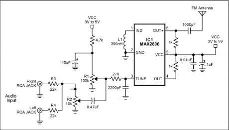
With MAX2606 we can make a small mono fm transmitter. It is build with MAX2606 and covers at least 20m with 1.5 m long copper wire antenna. You can use this transmitter as an oscillator but change the 1000pF capacitor from the antenna with 15pF.
MAX2606 transmitter output power is -10dBm, that means something around 100µW (micro-watts) = 0.0001W. Of course this is very low, that’s why we recommend you to use an auxiliary power amplifier if you want to build a more powerfull transmitter based on MAX2606. You can find a few fm power amplifiers on electroschematics.com so please use the search box.
Max2606 transmitter circuit diagram
(View)
View full Circuit Diagram | Comments | Reading(969)
Remote Tester Circuit
Published:2012/10/10 1:47:00 Author:muriel | Keyword: Remote Tester
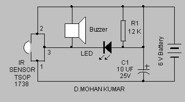
A simple Remote tester to check all types of Remote hand sets…….
This simple remote tester can be a good tool to check whether a remote hand set is working or not. It uses the commonly available IR sensor TSOP 1738.The IR sensor has a PIN photodiode and an FET signal amplifier enclosed in an Epoxy case.
The sensor requires five volts for its operation and its output is active low. Normally its output gives + 5 volts and goes down to zero when it receives 38 KHz pulsed IR rays. When the remote handset is focused on to the sensor and any one button is pressed, buzzer beeps and LED blinks indicating that the handset is OK.
Remote Tester Circuit Diagram
(View)
View full Circuit Diagram | Comments | Reading(2344)
Electronic Mail Box circuit
Published:2012/10/10 1:47:00 Author:muriel | Keyword: Electronic Mail Box
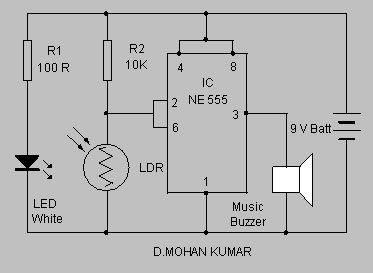
This Electronic Mail Box circuit generates music intimating the arrival of mail……..The circuit uses a high bright White LED and an LDR to detect the arrival of mail in the box. IC NE 555 is designed as a Schmitt trigger by shorting its trigger pin 2 and threshold pin 6. When the light from the LED illuminates the face of LDR, it conducts taking the pin 6 of IC low. Output pin 3 then remains low inhibiting the buzzer.When a mail falls between the LED and LDR, light from LED will be blocked and the LDR becomes non conducting. This makes the threshold pin of IC high and its output goes high. The high output makes buzzer active and music will be heard. The music stops only when the letter is removed from the box. Keep LED and LDR at the opposite sides of the box. (View)
View full Circuit Diagram | Comments | Reading(1499)
Electronic Locker Guard
Published:2012/10/10 1:46:00 Author:muriel | Keyword: Electronic Locker
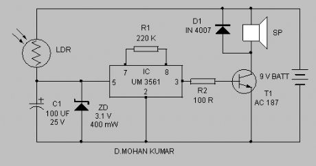
Protect your Locker or Briefcase from theft using this pocket sized gadget. It gives a loud police siren to catch attention.The circuit uses a single IC and a few discrete components. It works on the principle of light detection by LDR. When the unit is in dark, LDR cease to conduct and the alarm generator does not get power supply and it remains idle. When some one tries open the door of the locker, C1 charges via LDR. When the voltage in C1 raises to 3.1 volts, Zener conducts and gives power to IC UM 3561. It is a ROM IC that can generate different tones based on its pin connections. Here a police siren is selected by keeping pin6 floating. R1 determines the oscillation of IC. 220K (R1) is a must to give correct tone.C1 provides a lag of two minutes, so that the user gets sufficient time to disarm the unit.
Locker Guard Circuit Diagram
(View)
View full Circuit Diagram | Comments | Reading(1171)
PC FM Radio circuit
Published:2012/10/10 1:46:00 Author:muriel | Keyword: PC, FM Radio
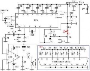
This is a fm radio receiver circuit which can be used with PC.PC radio REGULATIONSA) With the P1 we regulate the intensity of sound.B) With the P2 we regulate the frequency of reception.C) Optionally: If you want to check the frequency with your PC it will be supposed you make the following energies:- You assemble and the circuit that is in the blue frame.- You cut the driver dj’pla in point A, as it appears in the circuit and you connect points A,V.- If you know some language of programming as C ++, PASCAL, VISUAL BASIC, DELPHI etc you can write a program which will send in the parallel door (378 I) of PC a number from 0 until 255 checking thus the tendency of expense of simple D/A of converter (that it is in blue frame) and consequently and frequency of radio via passage VARICAP.(As long as grows the number that sends in the parallel door, so much minimizes the frequency that receives the radio.)Download DOS control program – radio fm pc dosPC FM receiver materials and circuit componentsThe resistances are 1/4W.R1 47KR2 22KR3 100KR4 39KR5 10R6-r12 7,5K – OptionallyR13-r21 15K – OptionallyP1 10K Logarithmic potentiometerP2 100K Linear potentiometerC1 39pF CeramicC2 47pF CeramicC3 2,2nF PolyesterC4, c14 220nF PolyesterC5 22nF PolyesterC6 10nF PolyesterC7, c18 180pF CeramicC8 150pF CeramicC9 100nF PolyesterC10, c13 330pF CeramicC11 220pF CeramicC12, c16 3300pF CeramicC15, c17 1800pF CeramicC19, c21, c22 10mF/16V electrolyticC20 10nF PolyesterC23 47nF PolyesterC24, c25 470mF/16V electrolytic capacitorL1, l2 5 Coils linked with internal diameter 4mm from cupreous isolated wire 0,6mm.IC1 TDA7000 with base DIL18IC2 LM7805IC3 LM386 with base DIL 8D1 BB329 or BB105 or other than old tuner televisions.SPEAKER Loudspeaker 8W/1W.S1 Switch of catering.AERIAL 50cm isolated wireCONNECTOR DB25 Fastener of 25 pin parallel door PC (LPT) -Optional
PC FM Radio circuit diagram
(View)
View full Circuit Diagram | Comments | Reading(3352)
Mobile Phone Travel Charger
Published:2012/10/10 1:46:00 Author:muriel | Keyword: Mobile Phone, Travel Charger
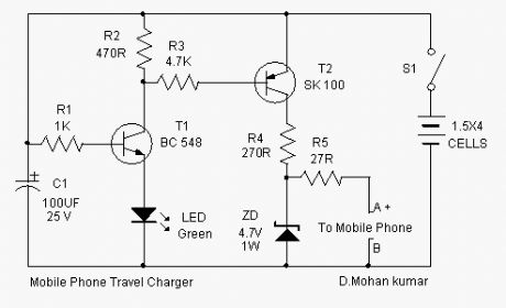
Here is an ideal Mobile charger using 1.5 volt pen cells to charge mobile phone while traveling. It can replenish cell phone battery three or four times in places where AC power is not available.Most of the Mobile phone batteries are rated at 3.6 V/500 mA. A single pen torch cell can provide 1.5 volts and 1.5 Amps current. So if four pen cells are connected serially, it will form a battery pack with 6 volt and 1.5 Amps current. When power is applied to the circuit through S1, transistor T1 conducts and Green LED lights.
When T1 conducts T2 also conducts since its base becomes negative. Charging current flows from the collector of T1. To reduce the charging voltage to 4.7 volts, Zener diode ZD is used. The output gives 20 mA current for slow charging. If more current is required for fast charging, reduce the value of R4 to 47 ohms so that 80 mA current will be available. Points A and B are used to connect the charger with the mobile phone. Use suitable pins for this and connect with correct polarity.
Mobile Phone Travel Charger Diagram
(View)
View full Circuit Diagram | Comments | Reading(1646)
The circuit of high-fidelity amplifier
Published:2012/10/9 22:30:00 Author:Ecco | Keyword: high-fidelity amplifier
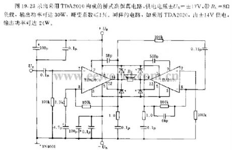
Figure 19.23 shows bridge high-fidelity circuit with TDA2010, and the supply voltage ± UB = ± 17V, load RL = 8Ω, output power can be up to 30W, the distortion coefficient ≤ 1 % . If the same circuit uses TDA2020, ± 14V power supply, the output power can be up to 24W.
(View)
View full Circuit Diagram | Comments | Reading(1537)
Monostable circuit using TcA965
Published:2012/10/9 22:06:00 Author:Ecco | Keyword: Monostable circuit
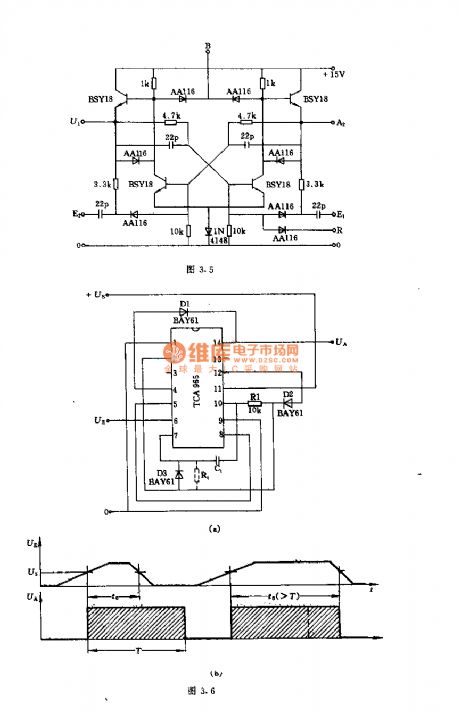
The integrated circuit TCA965's reference level U5 is provided by pin 8. If the input signal UE = U6 is less than U5 = U8, the output terminal pin 14 is in low level, and pin 2 is high ; if UE = U6 is high, then the corresponding U8 is decreased, the circuit makes the output flip. Figure b shows the input and output signal waveforms when output time is less( left) and greater (right ) than the monostable time constant. In the latter case, as long as UE = of U6 < U5, the output is immediately restored to low level.
(View)
View full Circuit Diagram | Comments | Reading(1509)
Quick Schmitt trigger circuit
Published:2012/10/9 21:55:00 Author:Ecco | Keyword: Quick, Schmitt, trigger
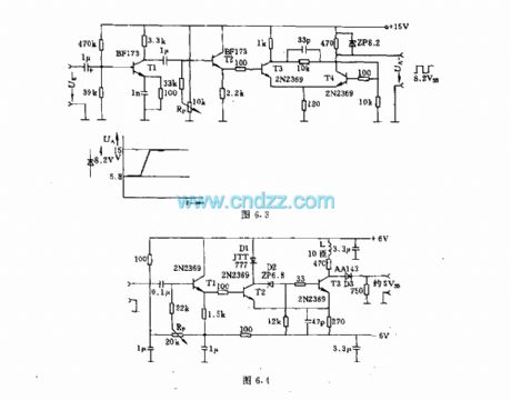
Adjustment potentiometer RP in circuit can adjust T1 emitter follower so as to change the base level of T2, so the trigger level can be adjusted continuously. In the switching process, 0.6VSS control signal on diode ITT777 is applied to the T3 base. The T2 collector potential is added to the T3 base by regulator ZP. This direct coupling way can eliminate the impact of the RC link.
(View)
View full Circuit Diagram | Comments | Reading(1218)
The circuit of measuring bridge amplifier
Published:2012/10/9 22:25:00 Author:Ecco | Keyword: Measuring bridge , amplifier

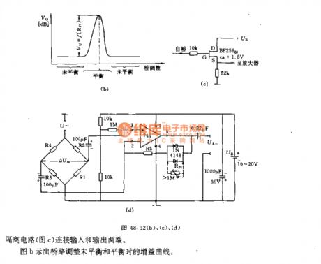
The measurement circuit shown in figure a is composed of resistors R1 ~ R4, the output voltage UBr may be DC or AC voltage ( up to 100kHz), if it is AC voltage, it can use capacitive coupling (Figure d ). In both cases, it can use high ohmic isolation circuit (Figure c) to connect to the input and output ends. Figure b shows unbalanced and balanced adjustment gain curve of bridge circuit.
(View)
View full Circuit Diagram | Comments | Reading(1217)
Fuse indicator circuit with light-emitting diode
Published:2012/10/9 21:15:00 Author:Ecco | Keyword: Fuse indicator , light-emitting diode
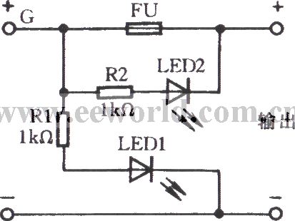
Motors and other electrical equipment commonly use fuse for over current and short circuit protection. But when the fuse blows, and it is not easy to detect. The circuit shown in Figure can timely inform the fuse blown. This is used for DC power fuse indicator. When the power output is normal, the current flows through R1, then LED1 is lit, it only shows that load work normally and supply polarity is normally. At this point, LED2 is fused and in short circuit without emitting light. When the fuse is blown, the current flowing through R2 makes LED2 light to indicate fuse failure.
(View)
View full Circuit Diagram | Comments | Reading(4501)
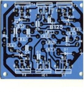
200W audio amplifier circuit
Published:2012/10/9 2:42:00 Author:muriel | Keyword: 200W, audio amplifier
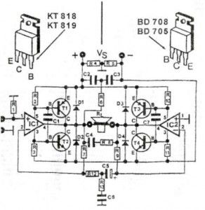
This audio amplifier circuit delivers up to 200 W of top-class quality for loudspeaker from 4 to 16 ohm. Operating voltage is between 24 and 36 V, max 5 A. The frequency response is from 20 to 20000 Hz.Please take special care that the transistors and the IC’s have been fixed firmly and solely one or two separated cooling elements with sufficient dimensions for this purpose (thermal resistance < 1K/W).
200W Power Amplifier circuit diagram
Doing so it is necessary to mount the transistors and the IC’s insulated (with mica washes and plastic nipple). Please make sure before first operation that the transistors and the IC’s really do not have any electrical connection towards the cooling plate! The transistors have to be placed plane and firmly onto the cooling element! It is of extraordinary importance with this high-power amplifier that there is a considerable heat dissipation. The already mounted cooling element should be situated in a well ventilated case.
The PSU should be sufficiently powerful, power consumption of the amplifier may increase up to 5A. In case of using an unstabilised power supply. It is advisable to place a transformer of max 28V.
The amplifier will the show approx. 120W at a 4-Ohm loudspeaker, for it no-load voltage of the power supply will not be to high. If it is desired to use complete power, it is necessary to place a stabilised power supply with approx. 36V 5A. No-load voltage should not pass over 44V!The cables leading the current supply and to the loudspeakers should have at least a cross section of min. 1.5 mm^2. The connected loudspeaker have to be equiped according to the high output power and should not have a lower impedance as 4 Ohm! With lower connection impedance and short circuit within the loudspeaker wiring, the transistors will be destructed.
The amplifier has an input sensitivity of approx. 500 … 800 mV. Therefore, it is possibile to connect directly at the amplifier tape decks, tuners, etc. In case there are connected signal sources with lower output voltage, it is necessary to pre-connect a preamplifier. Then it will alse be posible to connect microphones, etc.
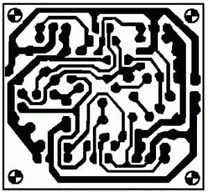
200W audio amplifier PCB
(View)
View full Circuit Diagram | Comments | Reading(1529)
The Art of Zener Regulation
Published:2012/10/9 2:42:00 Author:muriel | Keyword: Zener
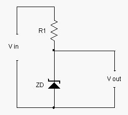
To get precise voltage to a circuit, the simplest and easy way is to use a Zener diode.It uses the reverse breakdown voltage characteristics to maintain a fixed voltage across it The Art of Zener Regulation
D.Mohan kumar
Zener diode ZD is used to generate a regulated DC output. A Zener diode is designed to operate in the reverse breakdown region. If a silicon diode is reverse biased, a point reached where its reverse current suddenly increases. The voltage at which this occurs is known as “Avalanche or Zener “value of the diode. Zener diodes are specially made to exploit the avalanche effect for use in ‘Reference voltage ‘regulators. A zener diode can be used to generate a fixed voltage by passing a limited current through it using the series resistor. The zener output voltage is not seriously affected by the resistor and the output remains as a stable reference voltage. But the limiting resistor is important, without which the zener diode will be destroyed. Even if the supply voltage varies, the series resistor will take up any excess voltage. The value of the series resistor can be calculated using the formula
R = Vin – Vz / Iz
Where Vin is the input voltage, Vz output voltage and Iz current through the zenerIn most circuits, Iz is kept as low as 5mA. If the supply voltage is 18V, the voltage that is to be dropped across R1 to get 12V output is 6volts. If the maximum zener current allowed is 100 mA, then R1 will pass the maximum desired output current plus 5 mA. So the value of R1 appears as
R1 = 18 – 12 / 105 mA = 6 / 105 x 1000 = 57 Ohms
Power dissipation
Power rating of the Zener is also an important factor to be considered while selecting the Zener diode. According to the formula P = IV. P is the power in watts, I current in Amps and V, the voltage. So the maximum power dissipation that can be allowed in a Zener is the Zener voltage multiplied by the current flowing through it. For example, if a 12V Zener passes 12 V DC and 100 mA current, its power dissipation will be 1.2 Watts. So a Zener diode rated 1.3W should be used.
As a rule of thumb, a minimum of 10% of the total current should flow the zener leaving the rest available to the load. By increasing the value of the series resistor, it is easy to reduce the current flowing through the zener but allow a minimum of 5 to 10 mA current through the zener. Then only it will reach the avalanche state to give output voltage.
(View)
View full Circuit Diagram | Comments | Reading(1060)
| Pages:309/2234 At 20301302303304305306307308309310311312313314315316317318319320Under 20 |
Circuit Categories
power supply circuit
Amplifier Circuit
Basic Circuit
LED and Light Circuit
Sensor Circuit
Signal Processing
Electrical Equipment Circuit
Control Circuit
Remote Control Circuit
A/D-D/A Converter Circuit
Audio Circuit
Measuring and Test Circuit
Communication Circuit
Computer-Related Circuit
555 Circuit
Automotive Circuit
Repairing Circuit