
Circuit Diagram
Index 308
The application circuit of single flashing light-emitting diode
Published:2012/10/10 21:39:00 Author:Ecco | Keyword: application, single , flashing light-emitting diode
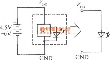
Flashing light-emitting diode operating frequency is only a few Hertz, and it is easy to attract attention, so it can be widely used in a variety of alarm circuits, such as temperature, liquid level and voltage -limit alarm circuit.
(View)
View full Circuit Diagram | Comments | Reading(1091)
ZKB8711 self-control alarm integrated circuit for thermostat automatic control alarm circuit
Published:2012/10/10 21:36:00 Author:Ecco | Keyword: self-control, alarm , integrated circuit, thermostat , automatic control , alarm
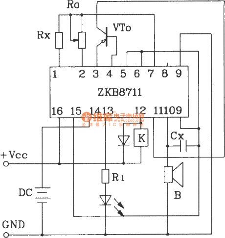
ZKB8711 can be used for temperature control, light control, rain control humidity control and hazardous gas detection alarm, the circuits with ZKB8711 have less external components, and they are easy to make.
(View)
View full Circuit Diagram | Comments | Reading(1626)
Level test circuit with TTL six NOT gate 7404
Published:2012/10/10 21:32:00 Author:Ecco | Keyword: Level test , TTL, six NOT gate
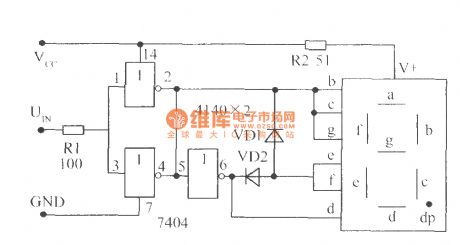
Because TTL ( CMOS ) circuit has determined high, low level input threshold voltage, it does not need additional set or adjust, and the result is very accurate. The two NAND gates of input end can be connected in parallel to increase drive capability, high level dispalys H, low level displays L. Due to they use common anode digital tube, VD1, VD2 polarity needs to be changed. If the CMOS level needs to be tested, you should use CMOS NAND gate circuit 4069.
(View)
View full Circuit Diagram | Comments | Reading(2126)
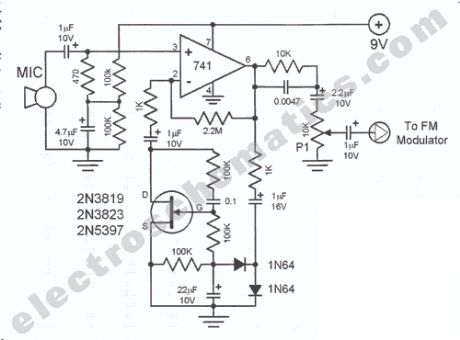
PLL transmitter circuit
Published:2012/10/10 2:00:00 Author:muriel | Keyword: PLL transmitter
The PLL transmitter exciter has the functions of providing a stable, low noise, frequency-selectable RF signal and amplify it to a controllable output power sufficient to drive the power amplifier. It uses a PLL frequency synthesizer built with MC145151, which covers the FM band in 100kHz steps. The VCO covers only a few MHz without readjustment. The pll transmitter output power is controllable from zero to 4 watts. A PLL unlock detector is included, to shut down the transmitter in the event of a malfunction. The Colpitts VCO is powered from a local 9V regulator, and has the frequency controlled by two back-to-back varactors, resulting in minimal loading and thus ultra low phase noise.
The output of the VCO goes through an emitter follower buffer stage, then through a broadly tuned class A amplifier, followed by a class B driver and a class C power amplifier, which use medium-Q tuned impedance matching networks. These last two stages are powered from a separate input, so that the output power of the Phase-Locked Loop transmitter can be controlled from zero to 4 W by adjusting this voltage from zero to 15V.
Note that the output of this pll module does not have enough harmonic filtering to connect it directly to an antenna. If you want to use this exciter as a stand-alone low power transmitter, you should add a low pass filter.
PLL transmitter circuit diagram
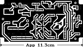
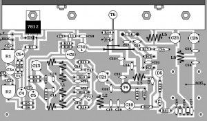
Phase-Locked Loop transmitter PCB
The Phase-Locked Loop transmitter is built on a double sided PCB, which has its top side copper left mostly undisturbed as a ground plane. The copper is removed only around non-grounded pins. The ground connections are soldered on the top side, so it’s not necessary to have plated-through holes.
This drawing shows the two sides of the PCB, so that you can print it and fold it in the middle to see how the two parts align. You will have to invert the image to print it for making the board, so that the ink gets in contact with the copper. This PCB is fitted with soldered shields all around and between stages, on both sides of the board. They are best installed before populating it. (View)
View full Circuit Diagram | Comments | Reading(929)
FM Radio Transmitter circuit
Published:2012/10/10 1:59:00 Author:muriel | Keyword: FM, Radio Transmitter
A simple fm radio transmitter circuit which covers frequencies from 88 to 108 MHz. It is built with 3 transistors: BC109, BFR91A and BFR96S. It is quite stable and the output power is around 200 mW.
The first stage in a mic amplifier but if you connect this radio transmitter directly to an audio source you can remove this stage and connect the audio signal to R5.U1, 1PH51C can be replaced with LM7805. You must use a stabilized power source for oscillator stage to prevent frequency variation. You can remove C7 and use a linear potentiometer insted of R6 with the median connector to C4, one pin to ground and the other one to +. You may replace BB109 varicap diode with BB139.
All coils must be perpendicular one to the other, especially L2 and L3. The oscillator stage must be encased with a copper 1mm foil. If you use an external antenna, like this fm dipole antenna connect it with a good coaxial cable because the power is low and you want to use most of it. If you don’t want to loose the rf power connect the radio transmitter close to the antenna (2 meter coaxial cable) and use a longer cable for the audio signal (coaxial). If you connect the antenna as I told you before you can cover a 300 meter in diameter area.
FM Radio Transmitter Circuit Diagram
(View)
View full Circuit Diagram | Comments | Reading(1750)
Electronic doorbell circuit
Published:2012/10/10 1:59:00 Author:muriel | Keyword: Electronic doorbell
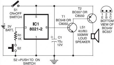
This simple and cost-effective ding dong electronic doorbell circuit is based on IC 8021-2. The IC has an in-built circuitry to produce ding dong sound each time its pin 3 is pulled low. The sound is stored in the IC as bits, as in a ROM. The sound output from the IC can’t however drive a speaker directly, as this puts strain on the device.Therefore a complementary-pair, two-transistor amplifier is used to amplify the sound to a fair level of audiblity. You may either use a piezo tweeter or an 8-ohm, 500mW speaker at the output. This simple electronic doorbell has not been tested.
During the standby period, the IC consumes nominal current of a few microamperes only. Therefore switch S1 may be kept closed. Each time switch S2 is pressed, ding dong sound is produced twice. If you try to press switch S2 a second time when the first ding dong sound is still being produed, it has no effect whatever and the two ding-dong bell sounds will be invariably produced.
Doorbell electronic circuit diagram
(View)
View full Circuit Diagram | Comments | Reading(2155)
Ultrasonic pest repellent circuit
Published:2012/10/10 1:59:00 Author:muriel | Keyword: Ultrasonic, pest repellent
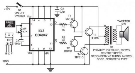
There are many ultrasonic pest repellent devices available on the market but a major drawback is that their power output is low and their effectiveness suffers. This electronic pest repellent generates powerful ultrasonic signals to repel pests.In addition to the ultrasonic frequency oscillator built with CD4047, separate push-pull power amplifier (with 2N3055 or TIP31C) and transformer are used to boost ultrasonic signals. The output of the power amplifier is coupled to a tweeter through output transformer X1, which is wound over ferrite core (UU or CC core).
Primary winding consists of 150 turns of 20 SWG while the secondary winding is 40 turns of 24 SWG wire. Adjust potentiometer VR1 for maximum effectiveness.This circuit has not been tested.
Caution! This is a powerful sonic pest repellent circuit so use it only in outdoor places. Do not use this ultrasonic pest repeller near babies or animal pets.
Pest repellent circuit diagram
(View)
View full Circuit Diagram | Comments | Reading(2532)
High Frequency Generator circuit
Published:2012/10/10 1:57:00 Author:muriel | Keyword: High Frequency, Generator
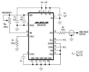
High frequency waveform generator is very useful in electronic experiment and design. This circuit generate sine wave oscillation, but actually we can modify the circuit to generate triangle or square wave function.The core of this waveform generator is MAX038. This integrated circuit chip gives complete function to build a waveform generator/function generator.
High frequency waveform generator circuit diagram
The circuit can be used to generate square wave, triangle, or sine wave by programming the pin inputs (A0:pin 3, A1:pin 4).
A0 A1 WAVEFORM
X 1 Sine wave
0 0 Square wave
1 0 Triangle wave
The frequency can be controlled using current. If we disconnect the 20k RIN from REF (pin 1) and connect it to a DAC, then we can control the frequency using microcontroller or digital interface. We can even control the chip using a quartz crystal (PLL) by controlling the current using a phase comparator output that compares the sync output (pin 14 of MAX038) and a reference clock from quartz crystal oscillator.
This waveform generator integrated circuit chip is very interesting since it can generate 0.1Hz to 20MHz, very wide operating frequency, as expected for every waveform generator instruments. (View)
View full Circuit Diagram | Comments | Reading(2084)
Automatic Night Lamp with Morning Alarm
Published:2012/10/10 1:57:00 Author:muriel | Keyword: Automatic, Night Lamp, Morning Alarm
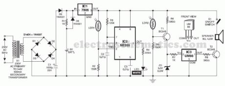
This circuit automatically turns on a night lamp when bedroom light is switched off. The lamp remains ON until the light sensor senses daylight in the morning. A super-bright white LED is used as the night lamp. It gives bright and cool light in the room. When the sensor detects the daylight in the morning, a melodious morning alarm sounds.The automatic night lamp circuit utilises light-dependant resistors (LDRs) for sensing darkness and light in the room. The resistance of LDR is very high in darkness, which reduces to minimum when LDR is fully illuminated. LDR1 detects darkness, while LDR2 detects light in the morning.
Night lamp circuit explanation
When LDR1 is illuminated with ambient light in the room, its resistance remains low, which keeps trigger pin 2 of IC2 at a positive potential. As a result, output pin 3 of IC2 goes low and the white LED remains off. As the illumination of LDR1’s sensitive window reduces, the resistance of the device increases.
In total darkness, the specified LDR has a resistance in excess of 280 kiloohms. When the resistance of LDR1 increases, a short pulse is applied to trigger pin 2 of IC2 via resistor R2 (150 kiloohms). This activates the monostable and its output goes high, causing the white LED to glow.
LDR2 and associated components generate the morning alarm at dawn. LDR2 etects the ambient light in the room at sunrise and its resistance gradually falls and transistor T1 starts conducting. When T1 conducts, melody-generator IC UM66 (IC3) gets supply voltage from the emitter of T1 and it starts producing the melody. The musical tone generated by IC3 is amplified by single-transistor amplifier T2. Resistor R7 limits the current to IC3 and zener diode ZD limits the voltage to a safer level of 3.3 volts.
The night lamp with alarm circuit can be easily assembled on a general-purpose PCB. Enclose it in a good-quality plastic case with provisions for LDR and LED. Use a reflective holder for white LED to get a spotlight effect for reading. Place LDRs away from the white LED, preferably on the backside of the case, to avoid unnecessary illumination. The speaker should be small so as to make the gadget compact.
Night lamp with alarm circuit diagram
(View)
View full Circuit Diagram | Comments | Reading(2092)
Audio Wattmeter circuit with LM3915
Published:2012/10/10 1:56:00 Author:muriel | Keyword: Audio Wattmeter circuit

You need an audio wattmeter to measure the power output of your audio amplifier?You need one LM3915 IC and add a few passive components and you got a simple but effective audio wattmeter.This sound wattmeter uses a row of colored LEDs as a scale to show the relative power output of your amplifier in watts. It is easy to be inserted into the speaker box. All you need is to hook a supply voltage to it. The value of R1 depends upon the impedance of the speaker being used. The table near the sound wattmeter diagram shows the necessary values of R1.
LM3915 audio wattmeter circuit diagram
If you want to apply the circuit to stereo systems you must build two identical circuits.
The supply voltage of the circuit is 12…20 volts/50 mA DC adapter. Take note that the LM3915 indicates only the positive swing of the signal. Anyway, by testing amplifiers it does not matter anyhow since a sine wave is normally used as a test signal. To test the circuit without using an actual speaker, you can connect a dummy resistor with a value of either 8 or 4 ohms.
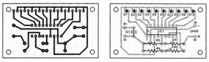
PCB layout and parts for the audio wattmeter
?
3 Responses to “Audio Wattmeter circuit with LM3915”
(View)
View full Circuit Diagram | Comments | Reading(3693)
HiFi Headphone Amplifier circuit
Published:2012/10/10 1:56:00 Author:muriel | Keyword: HiFi Headphone, Amplifier
This HiFi headphone amplifier circuit design is normally used to drive a headphone with a relative low impedance. It provides one watt power output and it can also be applied as an output stage for preamplifiers in conjuction with active loudspeakers boxes. The headphone amp is composed of an OP-AMP and an additional transistor amplifier. Input signals pass through a low pass filter composed of R1-C2. Its applification together with a relatively “fast” OPAMP provides a low distortion factor.The standby current is preset by diodes D1…D4 and R7-R8. The feedback resistors R3 and R4 set the amplification factor at about 15 dB. The distorsion factor is aound 0.1 % with a bandwidth of 10 Hz to 30 kHz.The headphone amplifier provides a maximum output of 1 watt to an 8 ohm load by an input level of 500 mV. High impedance headphones can be connected. The circuit can also drive a 4 ohm speaker.
Headphone amp circuit diagram
In order to prevent the output transistors from being destroyed in case of an output short circuit, they must be heatsinked. The transistors must also be electrically isolated from heatsink. Supply voltage can be provided by an adaptor with 6-8 volts DC output.
Headphones amplifier PCB layout
(View)
View full Circuit Diagram | Comments | Reading(2535)
Signal generator with thyristor
Published:2012/10/10 1:56:00 Author:muriel | Keyword: Signal generator
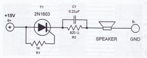
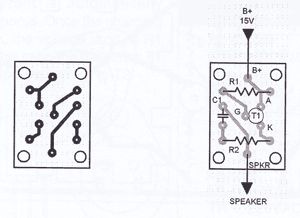
A very simple thyristor signal generator circuit which uses a single thyristor, two resistors, a capacitor and a mini-loudspeaker. Once the circuit is switched ti a current source, current flows through R1 and switches on the thyristor. The thyristor conducts current and chargers capacitor C.Since the charging current is inversely proportional to the charging of the capacitor, it slowly decreases until such a level that the thyristor switches off. Once the thyristor is off, capacitor C discharges through R2 and the whole process is repeated. The periodice switching on and off of the thyristor generates the oscillating signal. The frequency of the oscillation is determined by the C/R2 combination.
Signal generator circuit diagram and PCB layout
(View)
View full Circuit Diagram | Comments | Reading(1196)
Sound controlled lights
Published:2012/10/10 1:56:00 Author:muriel | Keyword: Sound controlled, lights
This sound controlled lights circuit design is used to control the brightness of the lights attached to it in sync with the sound that is being capturated by its microphone. This electronic circuit design is very common in disco houses, bars, parties …Usually, sound controlled lights are just connected in parallel with the loudspeakers. This configuration has two disadvantages: first, a very power amplifier can destroy the lights or worse, a defective light can destroy the amp. This problem is avoided by the circuit by not connecting directly to the amp. Instead, it picks up the sound with its microphone.
The power supply part is on the left of the electret microphone amplifier and the light controller part is on the right. The capacitors C2 and C3 are the capacitive voltage divider and reduces the power supply level. Diodes D1 and D2 rectify the positive swing of the AC voltage. The network composed of L1 and C1 protects the power line from voltages surges. In this circuit design, an electret microphone is being used. Take note that there are 2 types of electret mics. The first type has three pins for power, ground, and output. The second type has only two pins. The second type is used for this circuit.
Sound controlled light circuit diagram
In building this sound controlled lights circuit, take note that you are dealing with strong voltages and currents. The components used must have enough ratings to deal with those.The potentiometer P1, P2 and P3 must have plastic shafts and knobs. Use a shielded cable to connect the microphone to the circuit .
All wirings going to the main supply and lights must be isolated with shrink tubings. The case for the circuit must be made of plastic. Do not let anything metallic protrude out of the box.Even the heatsinks for the triacs are electrified. Beware that there is no isolation between this circuit and the main power lines. The maximum power output of each outpuc (triac) is 400 watts, do not exceed that level!
Audio controlled lights PCB Layout
(View)
View full Circuit Diagram | Comments | Reading(2459)
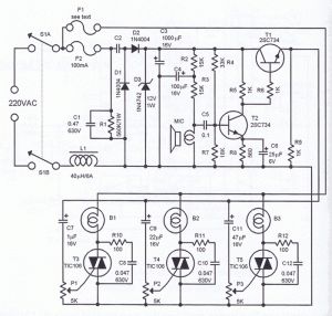
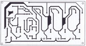
Auto Bathroom Fan control
Published:2012/10/10 1:55:00 Author:muriel | Keyword: Auto, Bathroom Fan
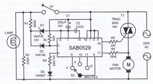
This auto bathroom fan control circuit design is a lamp and fan motor control with a delayed switch off. This automatic fan control is commonly used in toilet and bathrooms. When switch S1 is closed, the fan motor and the lamp turns on. When switch S1 is opened (switched off), the lamp goes out but the fan motor will keep running for another 3, 6 or 1 minutes linger (set by S2). This delayed switching off of the fan ensures that the unwanted odor is really fanned out the toilet.The heart of the bathroom exhaust fan circuit is the SAB0529 IC. It is a programmable extended time timer brought to the market by Siemens. This IC can be programmed to time from 1 second up to 31.5 hours. This extended time capacity is achieved by the IC by using the power line frequency as its time base.
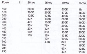
The bathroom fan light control circuit is commonly used to control inductive loads such as the case of fan motor. For this reason, a current synchronization is necessary. This is done with resistor R6. In addition, a capacitor C2 is connected between pins 15 and 1. This capacitor sets the pulse length at the output pin 16. If one decides to use a different triac, one needs to change the value of R5 . THis resistor sets the level of the trigger current, in this case 5 mA. The syc resistor R6 must be changed also. If the triac power and holding current (Ih) are known, one can get the value of R6 from the table below:
bathroom fan controller circuit diagram
(View)
View full Circuit Diagram | Comments | Reading(2655)
Car Antenna Amplifier circuit
Published:2012/10/10 1:55:00 Author:muriel | Keyword: Car Antenna, Amplifier
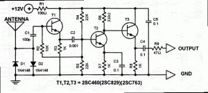
This car antenna amplifier can be used up to 70 MHz and is specially designed to boost the weak signals captured by the car antenna.It has a high input impedance and a low noise figure.
The total gain of the car antenna amplifier is around 30 dB and the input impedance at 30 Mhz is around 10 KΩ. The amplifier must be mounted directly at the base of the antenna to avoid signal losses caused by the capacitive character of the coaxial cable.This antenna amp must be used for non-mobile recievers. If you intend to install this circuit in you outdoor mounted antenna, make sure that is housed in a water proof case. Use this car antenna amp circuit only for receiver antennas. Transmitting through it will damage the components.
Car Antenna Amp Circuit Diagram
Antenna Amplifier PCB Layout
(View)
View full Circuit Diagram | Comments | Reading(1486)
Sawtooth Generator Circuit with 741 IC
Published:2012/10/10 1:54:00 Author:muriel | Keyword: Sawtooth Generator
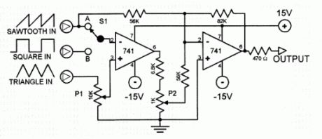
This sawtooth generator circuit use 741 IC and is used as a musical sound synthesizer. The sawtooth input signal is continously changed through P2 to a waveform with a doubled frequency and half amplitude. IC1 functions as a comparator and forms the sawtooth to a squarewave signal. IC2 serves as a adder.The input signal and the converted signal are mixed to create the output signal. An additional LFO pulsewidth modulated the squarewave to give the output sound the desired effect. When switch S1 is switched to position B, the squarewave can be mixed with a freq. which is independent from the sawtooth.The current consumption is around 10 mA.
Sawtooth Generator Circuit Diagram
(View)
View full Circuit Diagram | Comments | Reading(2868)
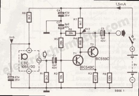
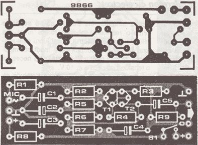
Electret microphone amplifier circuit
Published:2012/10/10 1:53:00 Author:muriel | Keyword: Electret microphone, amplifier
This article describes an compact electret microphone amplifier but you can connect dynamic microphones with low resistance. Electret microphones can be inserted in the same box with the amplifier, it only need 5 to 10V or 9V battery with a current consumption of just 1.5mA.
Electret microphone amplifier circuit
Electret mic amplifier pcb
(View)
View full Circuit Diagram | Comments | Reading(2867)
Rf 15W – 30W power amplifier KT922, KT930, KT934
Published:2012/10/10 1:53:00 Author:muriel | Keyword: Rf, 15W – 30W, power amplifier
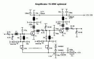
This rf amplifier ensure the power you need to boost a small transmitter.Depending of input rf power, power supply and transistor, this amplifier can boost from 15W up to 30W.The most important components : 7805, 1N4001 diodes mounted in series, 120 ohm / 2W resistor and 1N4145 diodes.The setup : trim P (220 ohm ) untill you obtain 50mA thru T1 and 100mA thru T2. Without any input signal you must measure 1.5V like in the schematic, if the voltage is higher the 2 transistors can burn.At 12V and 0.1W input rf power the output is 6W and with 0.5W the output is 15W.At 24V and 0.1W input power the output is 10W and with 0.5W the output is 25W.
RF power amplifier circuit diagram
(View)
View full Circuit Diagram | Comments | Reading(2183)
Automatic Gain Control – AGC circuit
Published:2012/10/10 1:52:00 Author:muriel | Keyword: Automatic, Gain Control
Automatic Gain Control or AGC is a circuit design which maintain the same level of amplification for sound or radio frequency. If the signal is too low the AGC circuit will increase (amplify) the level and if is to high will lower it to maintain a constant level as possible. The Automatic Gain Control principle is widely use in AM receivers and sometimes AGC is called an compressor-expander because it acts just like one.On the electroschematics.com site you can find some AGC schematics, just use the seach box.
Mic preamplifier with AGC schematic
(View)
View full Circuit Diagram | Comments | Reading(2594)
Veronica 1W Fm transmitter circuit
Published:2012/10/10 1:51:00 Author:muriel | Keyword: 1W, Fm transmitter
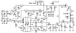
Veronica 1W FM transmitter is easy to build and to operate in FM. Veronica is also known for frequency stability, clean fm signal and uses no integrated circuit.You may want to check this another 1W FM transmitter circuit.Veronica transmitter is equiped with a mini-mixer and so you may forget an external mixer. This consist from T1 transistor wich amplifies the microphone signal before it is combined with cd-player audio or pc signal. R1 and R2 are potentiometers ( variable resistors ) used to adjust the audio level.The component between R8 and C21 represents the oscillator wich generates radio signal. D1 is a varicap diode ( like a variable capacitor or trimmer) controlled by audio signal. C12, C13 and L1 decides the frequency.The Veronica oscillator is actually formed from 2 oscillators wich operates somewhere arround 50 MHz in antiphase and the 2 signals are combined to form 100MHz fm radio signal. This kind of circuit design is stabile and is amplified up to 1W by T4 2n4427
Veronica transmitter 1 watt circuit
Veronica components listResistors:R1+2 10k potR3 820kR4 4.7kR5-7+19 220rR8 1.5kR9 15kR10+11 1kR12 33kR13+14 56rR15+16 68kR17 47rR18 270rR20 10kCapacitorsC1, 2, 7, 16, 17, 19,24, 29 & 31 1nC3-5 & 8 10u elect.C6, 18 & 30 220u elect.C9, 10 & 20 10nC11 22p*C12 47p*C13 22p trimmerC14 & 15 15p*C21, C25 & 26 65p trimmerC22 100pC23 5.6pC27 & 28 1.8pCoilsL1 – 6 coils / 2 turns, 5mm diam si 5mm lengthL2 – 3 turns, 7mm diam si 7mm lengthL3 – 4 turns, 5mm diam si 7mm lengthL4 – 6 turns, 5mm diam si 10mm lengthDiodeD1 KV1310D2+3 1N4148D4 Standard LEDD5 1N4001TransistorsT1+5 BC548T2+3 BF494T4 2N4427
The transmitter must be mounted in an aluminium carcase connected to ground. The power supply voltage is between 9 and 16V, at 16V the rf output power is 1W and at 12V is 600mW and at 9V is 200mW
Veronica PCB and components layout
(View)
View full Circuit Diagram | Comments | Reading(2883)
| Pages:308/2234 At 20301302303304305306307308309310311312313314315316317318319320Under 20 |
Circuit Categories
power supply circuit
Amplifier Circuit
Basic Circuit
LED and Light Circuit
Sensor Circuit
Signal Processing
Electrical Equipment Circuit
Control Circuit
Remote Control Circuit
A/D-D/A Converter Circuit
Audio Circuit
Measuring and Test Circuit
Communication Circuit
Computer-Related Circuit
555 Circuit
Automotive Circuit
Repairing Circuit