
Circuit Diagram
Index 300
Automatic 12 Volt Lamp Fader
Published:2012/10/18 22:44:00 Author:muriel | Keyword: Automatic, 12 Volt, Lamp Fader
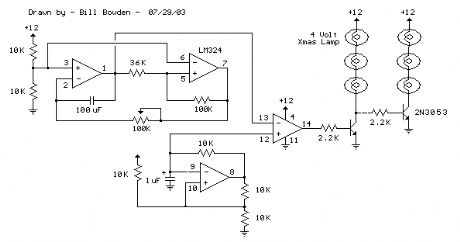
This circuit is similar to the Fading Red Eyes circuit (in the LED section) used to fade a pair of red LEDs. In this version, the lamps are faded by varying the duty cycle so that higher power incandescent lamps can be used without much power loss. The switching waveform is generated by comparing two linear ramps of different frequencies. The higher frequency ramp waveform (about 75 Hz.) is produced from one section of the LM324 quad op-amp wired as a Schmitt trigger oscillator. The lower frequency ramp controls the fading rate and is generated from the upper two op-amps similar to the fading eyes circuit. The two ramp waveforms at pins 9 and 1 are compared by the 4th op-amp which generates a varying duty cycle rectangular waveform to drive the output transistor. A second transistor is used to invert the waveform so that one group of lamps will fade as the other group brightens. The 2N3053 will handle up to 500 milliamps so you could connect 12 strings of 4 LEDs each (48 LEDs) with a 220 ohm resistor in series with each group of 4 LEDs. This would total about 250 milliamps. Or you can use three 4 volt, 200 mA Xmas tree bulbs in series. For higher power 12 volt automobile lamps, the transistor will need to be replaced with a MOSFET that can handle several amps of current. See the drawing below the schematic for possible hookups. (View)
View full Circuit Diagram | Comments | Reading(1029)
12 Volt Lamp Dimmer
Published:2012/10/18 22:43:00 Author:muriel | Keyword: 12 Volt, Lamp Dimmer
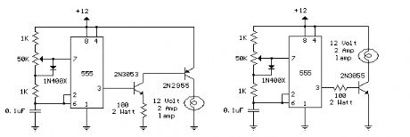
Here is a 12 volt / 2 amp lamp dimmer that can be used to dim a standard 25 watt automobile brake or backup bulb by controlling the duty cycle of a astable 555 timer oscillator. When the wiper of the potentiometer is at the uppermost position, the capacitor will charge quickly through both 1K resistors and the diode, producing a short positive interval and long negative interval which dims the lamp to near darkness. When the potentiometer wiper is at the lowermost position, the capacitor will charge through both 1K resistors and the 50K potentiometer and discharge through the lower 1K resistor, producing a long positive interval and short negative interval which brightens the lamp to near full intensity. The duty cycle of the 200 Hz square wave can be varied from approximately 5% to 95%. The two circuits below illustrate connecting the lamp to either the positive or negative side of the supply. (View)
View full Circuit Diagram | Comments | Reading(1082)
FM Beacon Broadcast Transmitter (88-108 MHz)
Published:2012/10/18 22:42:00 Author:muriel | Keyword: FM , Beacon Broadcast , Transmitter, 88-108 MHz
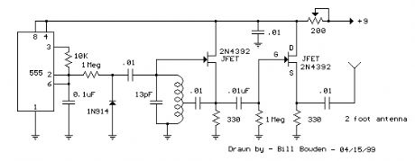
This circuit will transmit a continuous audio tone on the FM broadcast band (88-108 MHz) which could used for remote control or security purposes. Circuit draws about 30 mA from a 6-9 volt battery and can be received to about 100 yards. A 555 timer is used to produce the tone (about 600 Hz) which frequency modulates a Hartley oscillator. A second JFET transistor buffer stage is used to isolate the oscillator from the antenna so that the antenna position and length has less effect on the frequency. Fine frequency adjustment can be made by adjusting the 200 ohm resistor in series with the battery. Oscillator frequency is set by a 5 turn tapped inductor and 13 pF capacitor. The inductor was wound around a #8 X 32 bolt (about 3/16 diameter) and then removed by unscrewing the bolt. The inductor was then streached to about a 3/8 inch length and tapped near the center. The oscillator frequency should come out somewhere near the center of the band (98 MHz) and can be shifted higher or lower by slightly expanding or compressing the inductor. A small signal diode (1N914 or 1N4148) is used as a varactor diode so that the total capacity in parallel with the inductor varies slightly at the audio rate thus causing the oscillator frequency to change at the audio rate (600 Hz). The ramping waveform at pins 2 and 6 of the timer is applied to the reversed biased diode through a large (1 Meg) resistor so that the capacitance of the diode changes as the ramping voltage changes thus altering the frequency of the tank circuit. Alternately, an audio signal could be applied to the 1 Meg resistor to modulate the oscillator but it may require an additional pullup resistor to reverse bias the diode. The N channel JFET transistors used should be high frequency VHF or UHF types (Radio Shack #276-2062 MPF102) or similar. (View)
View full Circuit Diagram | Comments | Reading(1005)
Micro Power AM Broadcast Transmitter
Published:2012/10/18 22:40:00 Author:muriel | Keyword: Micro Power, AM , Broadcast Transmitter

In this circuit, a 74HC14 hex Schmitt trigger inverter is used as a square wave oscillator to drive a small signal transistor in a class C amplifier configuration. The oscillator frequency can be either fixed by a crystal or made adjustable (VFO) with a capacitor/resistor combination. A 100pF capacitor is used in place of the crystal for VFO operation. Amplitude modulation is accomplished with a second transistor that controls the DC voltage to the output stage. The modulator stage is biased so that half the supply voltage or 6 volts is applied to the output stage with no modulation. The output stage is tuned and matched to the antenna with a standard variable 30-365 pF capacitor. Approximately 20 milliamps of current will flow in the antenna lead (at frequencies near the top of the band) when the output stage is optimally tuned to the oscillator frequency. A small 'grain of wheat' lamp is used to indicate antenna current and optimum settings. The 140 uH inductor was made using a 2 inch length of 7/8 inch (OD) PVC pipe wound with 120 turns of #28 copper wire. Best performance is obtained near the high end of the broadcast band (1.6 MHz) since the antenna length is only a very small fraction of a wavelength. Input power to the amplifier is less than 100 milliwatts and antenna length is 3 meters or less which complies with FCC rules. Output power is somewhere in the 40 microwatt range and the signal can be heard approximately 80 feet. Radiated power output can be approximated by working out the antenna radiation resistance and multiplying by the antenna current squared. The radiation resistance for a dipole antenna less than 1/4 wavelength is
R = 80*[(pi)^2]*[(Length/wavelength)^2]*(a factor depending on the form of the current distribution) The factor depending on the current distribution turns out to be [(average current along the rod)/(feed current)]^2 for short rods, which is 1/4 for a linearly-tapered current distribution falling to zero at the ends. Even if the rods are capped with plates, this factor cannot be larger than 1. Substituting values for a 9.8 foot dipole at a frequency of 1.6 MHz we get R= 790*.000354*.25 = .07 Ohms. And the resistance will be only half as much for a monopole or 0.035 Ohms. Radiated power at 20 milliamps works out to about I^2 * R = 14 microwatts.
(View)
View full Circuit Diagram | Comments | Reading(2498)
Reading Data From The Parallel Port
Published:2012/10/18 22:39:00 Author:muriel | Keyword: Parallel Port
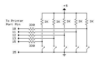
The diagram below shows 5 switches connected to the 5 input lines of the parallel port. An external 5 volt power supply is used to provide high logic levels to the input pins when the switches are open. Three 1.5 volt batteries in series can be used to obtain 4.5 volts which is close enough. The 330 ohm resistors in series with the port connections provide some protection in case a connection is made to the wrong pin. If you are sure of the connections, the 330 ohm resistors can be left out and the switches connected directly to the input pins. The negative side of the power supply should be connected to the ground point, or any pin from 18 to 25.
The following short QBasic program can be used to read the state of the switches. QBASIC.EXE can be found in the OLDMSDOS directory of the Windows 95/98 CD Rom. Note that there are three possible printer port address that correspond to LPT1, LPT2 and LPT3 and LPT1 is usually the one to use which is at address decimal 889. The program waits for the user to press the enter key before reading the state of the 5 input lines. The state of the 5 lines is received as a single 8 bit number between 0-255 which is stored as the value of (V). Each switch input represents a decimal value of 8,16,32,64 and 128 which correspond to pins 15,13,12,10 and 11. The last 3 bits (1,2 and 4) are not used and should return a high level, so the value received with all switches open should be 1+2+4+8+16+32+64=127. If a switch is closed and the input is at ground, the value will be 0 except for pin 11 which is inverted and yields a value of 128 and 0 when high, so the value received when all switches are closed should be 1+2+4+128=135. (View)
View full Circuit Diagram | Comments | Reading(1215)
Parallel Port Relay Interface
Published:2012/10/18 22:39:00 Author:muriel | Keyword: Parallel Port, Relay Interface
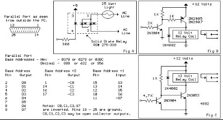
Below are three examples of controlling a relay from the PC's parallel printer port (LPT1 or LPT2). Figure A shows a solid state relay controlled by one of the parallel port data lines (D0-D7) using a 300 ohm resistor and 5 volt power source. The solid state relay will energize when a 0 is written to the data line. Figure B and C show mechanical relays controlled by two transistors. The relay in figure B is energized when a 1 is written to the data line and the relay in figure C is energized by writing a 0 to the line. In each of the three circuits, a common connection is made from the negative side of the power supply to one of the port ground pins (18-25).
There are three possible base addresses for the parallel port You may need to try all three base addresses to determine the correct address for the port you are using but LPT1 is usually at Hex 0378. The QBasic OUT command can be used to send data to the port. OUT, &H0378,0 sets D0-D7 low and OUT, &H378,255 sets D0-D7 high. The parallel port also provides four control lines (C0,C1,C2,C3) that can be set high or low by writing data to the base address+2 so if the base address is Hex 0378 then the address of the control latch would be Hex 037A. Note that three of the control bits are inverted so writing a 0 to the control latch will set C0,C1,C3 high and C2 low. (View)
View full Circuit Diagram | Comments | Reading(1796)
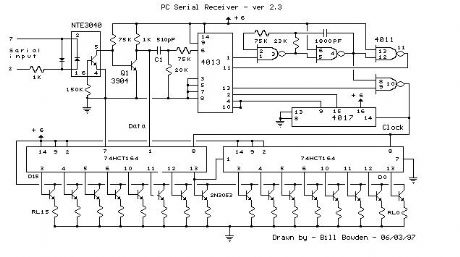
PC Serial Receiver (57.6K Baud / TTL & CMOS)
Published:2012/10/18 22:34:00 Author:muriel | Keyword: PC , Serial Receiver , 57.6K Baud , TTL & CMOS
View full Circuit Diagram | Comments | Reading(813)
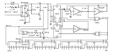
PC Serial Port Receiver
Published:2012/10/18 22:33:00 Author:muriel | Keyword: PC , Serial Port , Receiver
This circuit was designed to control a 32 channel Christmas light show from the PC serial port. Originally designed with TTL logic, it has been simplified using CMOS circuits to reduce component count. It is a fairly simple, reliable circuit that requires only 4 common CMOS chips (for 8 outputs), an optical isolator, and a few discrete components. The schematic diagram (SERIAL.GIF) illustrates the circuit with 16 outputs which can be expanded with additional 8 bit shift registers. (View)
View full Circuit Diagram | Comments | Reading(1174)
Low Power Op-Amp - Audio Amp (50 milliwatt)
Published:2012/10/18 22:23:00 Author:muriel | Keyword: Low Power, Op-Amp , Audio Amp , 50 milliwatt
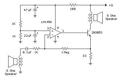
The example below illustrates using an op-amp as an audio amplifier for a simple intercom. A small 8 ohm speaker is used as a microphone which is coupled to the op-amp input through a 0.1uF capacitor. The speaker is sensitive to low frequencies and the small value capacitor serves to attenuate the lower tones and produce a better overall response. You can experiment with different value capacitors to improve the response for various speakers. The op-amp voltage gain is determined by the ratio of the feedback resistor to the series input resistor which is around one thousand in this case (1 Meg / 1K). The non-inverting input (pin 3) to the op-amp is biased at 50% of the supply voltage (4.5 volts) by a couple 1K resistors connected across the supply. Since both inputs will be equal when the op-amp is operating within it's linear range, the voltage at the inverting input (pin 2) and the emitter of the buffer transistor (2N3053) will also be 4.5 volts. The voltage change at the emitter of the transistor will be around +/- 2 volts for a 2 millivolt change at the input (junction of 0.1 cap and 1K resistor) which produces a current change of about 2/33 = 60 mA through the 33 ohm emitter resistor and the speaker output. The peak output speaker power is about I^2 * R or .06 ^2 * 8 = 28 milliwatts. The 100 resistor and 47uF capacitor are used to isolate the op-amp from the power supply and reduce the possibility of oscillation. An additional 22uF cap is used at the non-inverting input to further stabilize operation. These parts may not be needed in such a low power circuit but it's a good idea to decouple the power supply to avoid unwanted feedback. The circuit draws about 1.2 watts from a 9 volt source and is not very efficient but fairly simple to put together. The circuit was tested using a couple 4 inch speakers located a few feet apart (to reduce feedback) and a small pocket transistor radio placed on top of the speaker/microphone as an audio source. (View)
View full Circuit Diagram | Comments | Reading(2437)
Single Op-Amp Bandpass Filter
Published:2012/10/18 3:44:00 Author:muriel | Keyword: Single, Op-Amp , Bandpass Filter
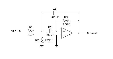
A bandpass filter passes a range of frequencies while rejecting frequencies outside the upper and lower limits of the passband. The range of frequencies to be passed is called the passband and extends from a point below the center frequency to a point above the center frequency where the output voltage falls about 70% of the output voltage at the center frequency. These two points are not equally spaced above and below the center frequency but will look equally spaced if plotted on a log graph. The percentage change from the lower point to the center will be the same as from the center to the upper, but not the absolute amount. This is similar to a musical keyboard where each key is separated from the next by the same percentage change in frequency, but not the absolute amount.
The filter bandwidth (BW) is the difference between the upper and lower passband frequencies. A formula relating the upper, lower, and center frequencies of the passband is:
Center Frequency = Square Root of (Lower Frequency * Upper Frequency)
The quality factor, or Q of the filter is a measure of the distance between the upper and lower frequency points and is defined as (Center Frequency / BW) so that as the passband gets narrower around the same center frequency, the Q factor becomes higher. The quality factor represents the sharpness of the filter, or rate that the amplitude falls as the input frequency moves away from the center frequency during the first octave. As the frequency gets more than one octave away from center frequency the rollof approaches 6 dB per octave regardless of Q value. Approximate rolloff rates for different Q values for a single octave change from center frequency are:
Q = 1 = 6 dB Q = 5 = 18 dB Q = 10 = 24 dB Q = 50 = 40 dB
For a single op-amp bandpass filter with both capacitors the same value, the Q factor must be greater than the square root of half the gain, so that a gain of 98 would require a Q factor of 7 or more.
The example below shows a 1700 Hz bandpass filter with a Q of 8 and a gain of 65 at center frequency (1700 Hz). Resistor values for the filter can be worked out using the three formulas below. Both capacitor values need to be the same for the formulas to work and are chosen to be 0.01uF which is a common value usable at audio frequencies. This same filter is used in the Whistle On / Whistle Off relay toggle circuit.
R1 = Q / (G*C*2*Pi*F) = 8/(65 * .00000001 * 6.28 * 1700) = 1152 or 1.1K R2 = Q / ((2*Q^2)-G)*C*2*Pi*F) = 8/((128-65) * .00000001 * 6.28 * 1700) = 1189 or 1.2K R3 = (2*Q) / (C*2*Pi*F) = 16 / (.00000001 * 6.28 * 1700) = 150K (View)
View full Circuit Diagram | Comments | Reading(2181)
Operational Amplifier (Op-Amp) Basics
Published:2012/10/18 3:43:00 Author:muriel | Keyword: Operational Amplifier
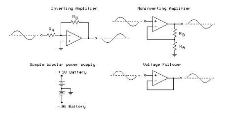
The op-amp is basically a differential amplifier having a large voltage gain, very high input impedance and low output impedance. The op-amp has a inverting or (-) input and noninverting or (+) input and a single output. The op-amp is usually powered by a dual polarity power supply in the range of +/- 5 volts to +/- 15 volts. A simple dual polarity power supply is shown in the figure below which can be assembled with two 9 volt batteries.
Inverting Amplifier:
The op-amp is connected using two resistors RA and RB such that the input signal is applied in series with RA and the output is connected back to the inverting input through RB. The noninverting input is connected to the ground reference or the center tap of the dual polarity power supply. In operation, as the input signal moves positive, the output will move negative and visa versa. The amount of voltage change at the output relative to the input depends on the ratio of the two resistors RA and RB. As the input moves in one direction, the output will move in the opposite direction, so that the voltage at the inverting input remains constant or zero volts in this case. If RA is 1K and RB is 10K and the input is +1 volt then there will be 1 mA of current flowing through RA and the output will have to move to -10 volts to supply the same current through RB and keep the voltage at the inverting input at zero. The voltage gain in this case would be RB/RA or 10K/1K = 10. Note that since the voltage at the inverting input is always zero, the input signal will see a input impedance equal to RA, or 1K in this case. For higher input impedances, both resistor values can be increased.
Noninverting Amplifier:
The noninverting amplifier is connected so that the input signal goes directly to the noninverting input (+) and the input resistor RA is grounded. In this configuration, the input impedance as seen by the signal is much greater since the input will be following the applied signal and not held constant by the feedback current. As the signal moves in either direction, the output will follow in phase to maintain the inverting input at the same voltage as the input (+). The voltage gain is always more than 1 and can be worked out from Vgain = (1+ RB/RA).
Voltage Follower:
The voltage follower, also called a buffer, provides a high input impedance, a low output impedance, and unity gain. As the input voltage changes, the output and inverting input will change by an equal amount. (View)
View full Circuit Diagram | Comments | Reading(1171)
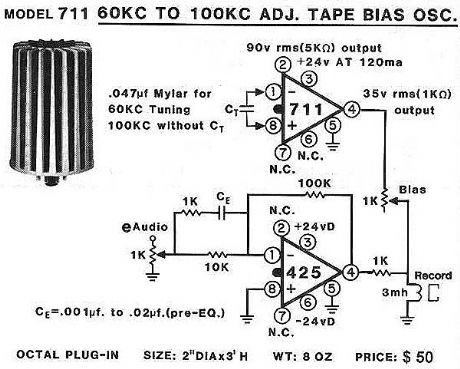
60 to 100kHz Adj. Tape Bias Oscillator -
Published:2012/10/18 3:41:00 Author:muriel | Keyword: 60 to 100kHz, Adj. , Tape Bias Oscillator
View full Circuit Diagram | Comments | Reading(2925)
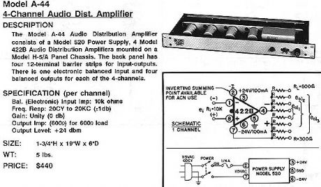
4-chanel audio dist. amplifier
Published:2012/10/18 3:40:00 Author:muriel | Keyword: 4-chanel, audio dist. amplifier
View full Circuit Diagram | Comments | Reading(889)
4-input summing power amplifier
Published:2012/10/18 3:37:00 Author:muriel | Keyword: 4-input, summing power, amplifier
View full Circuit Diagram | Comments | Reading(857)
OpAmp Stall-Motor Switch Machine Drivers
Published:2012/10/18 3:33:00 Author:muriel | Keyword: OpAmp, Stall-Motor Switch, Machine Drivers
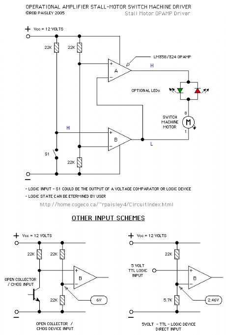
The circuits on this page are switch machine drivers that can be used to operate Stall-Motor type switch machine motors. The circuits use LM324 Quad or 358 Dual operational Amplifier chips to provide a PUSH-PULL output to reverse the polarity of the supply to the switch machine motors.
The drivers use direct control inputs such as switches or CMOS and TTL logic devices.
The advantage of this type of driver is low cost and, in the case of the 324, two drivers per package can be built. These operational amplifiers can only supply enough output current to drive one switch machine per driver. (View)
View full Circuit Diagram | Comments | Reading(1174)
25hz peaking amplifier
Published:2012/10/18 3:32:00 Author:muriel | Keyword: 25hz, peaking amplifier
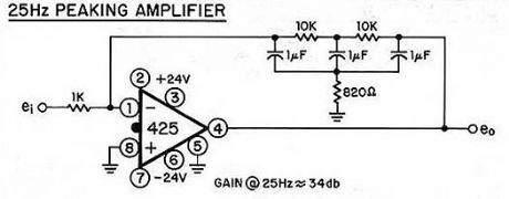
View full Circuit Diagram | Comments | Reading(876)
2-wire remote microphone
Published:2012/10/18 3:31:00 Author:muriel | Keyword: 2-wire, remote microphone
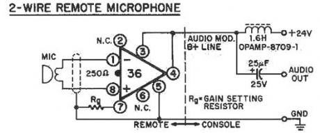
View full Circuit Diagram | Comments | Reading(4726)
100MHz Op Amp LT6203
Published:2012/10/18 3:30:00 Author:muriel | Keyword: 100MHz, Op Amp, LT6203
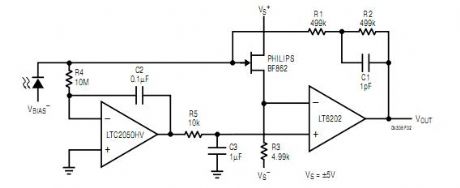

In this case however, the JFET is not allowed to dictate the DC bias conditions. Instead of simply grounding the LT6202 noninverting input, an LTC2050 drives it (and therefore the source) exactly to where it needs to be for zero JFET gate voltage. The addition of the LTC2050 increases the total supply current by about 1mA. (View)
View full Circuit Diagram | Comments | Reading(1399)
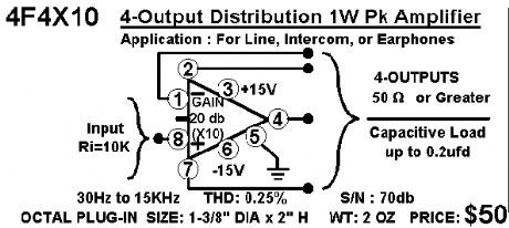
4-output distribution 1W pk amplifier
Published:2012/10/18 3:28:00 Author:muriel | Keyword: 4-output, distribution, 1W, pk amplifier

View full Circuit Diagram | Comments | Reading(1003)
Unusual Radar Detector - This unique anchient design uses a chopper amplifier
Published:2012/10/18 3:26:00 Author:muriel | Keyword: Unusual, Radar Detector
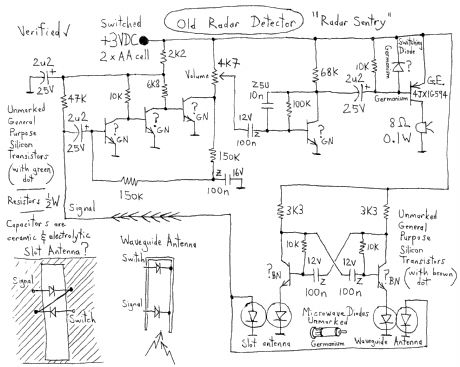
The microwave diodes are chopper-gated by a multivibrator so the RF signal level can be detected by an audio frequency amplifier. (View)
View full Circuit Diagram | Comments | Reading(3705)
| Pages:300/2234 At 20281282283284285286287288289290291292293294295296297298299300Under 20 |
Circuit Categories
power supply circuit
Amplifier Circuit
Basic Circuit
LED and Light Circuit
Sensor Circuit
Signal Processing
Electrical Equipment Circuit
Control Circuit
Remote Control Circuit
A/D-D/A Converter Circuit
Audio Circuit
Measuring and Test Circuit
Communication Circuit
Computer-Related Circuit
555 Circuit
Automotive Circuit
Repairing Circuit