
Circuit Diagram
Index 295
Generating a Delayed Pulse Using The 555 Timer
Published:2012/10/23 20:21:00 Author:muriel | Keyword: Delayed Pulse, 555 Timer

The circuit below illustrates generating a single positive pulse which is delayed relative to the trigger input time. The circuit is similar to the one above but employs two stages so that both the pulse width and delay can be controlled. When the button is depressed, the output of the first stage will move up and remain near the supply voltage until the delay time has elapsed, which in this case is about 1 second. The second 555 stage will not respond to the rising voltage since it requires a negative, falling voltage at pin 2, and so the second stage output remains low and the relay remains de-energized. At the end of the delay time, the output of the first stage returns to a low level, and the falling voltage causes the second stage to begin it's output cycle which is also about 1 second as shown. This same circuit can be built using the dual 555 timer which is a 556, however the pin numbers will be different. (View)
View full Circuit Diagram | Comments | Reading(1784)
555 timer Mono stable (one shot) circuit
Published:2012/10/23 20:20:00 Author:muriel | Keyword: 555 timer , Mono stable, one shot
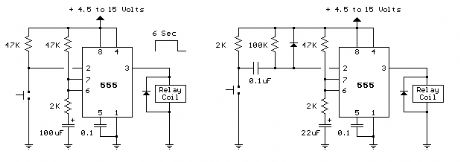
The two circuits below illustrate using the 555 timer to close a relay for a predetermined amount of time by pressing a momentary N/O push button. The circuit on the left can be used for long time periods where the push button can be pressed and released before the end of the timing period. For shorter periods, a capacitor can be used to isolate the switch so that only the initial switch closure is seen by the timer input and the switch can remain closed for an unlimited period without effecting the output.
In the idle state, the output at pin 3 will be at ground and the relay deactivated. The trigger input (pin 2) is held high by the 100K resistor and both capacitors are discharged. When the button is closed, the 0.1uF cap will charge through the button and the 100K resistor which causes the voltage at pin 2 to move low for a few milliseconds. The falling voltage at pin 2 triggers the 555 and starts the timing cycle. The output at pin 3 immediately moves up to near the supply voltage (about 10.4 volts for a 12 volt supply) and remains at that level until the 22 uF timing capacitor charges to about 2/3 of the supply voltage (about 1 second as shown). Most 12 volt relays will operate at 10.4 volts, if not, the supply voltage could be raised to 13.5 or so to compensate. The 555 output will supply up to 200mA of current, so the relay could be replaced with a small lamp, doorbell, or other load that requires less than 200mA. When the button is released, the 0.1uF capacitor discharges through the 100K and 2K resistors. The diode across the 100K resistor prevents the voltage at pin 2 from rising above the supply voltage when the cap discharges. The 2K resistor in series with the 22uF cap limits the discharge current from pin 7 of the timer. This resistor may not be necessary, but it's a good idea to limit current when discharging capacitors across switch contacts or transistors. (View)
View full Circuit Diagram | Comments | Reading(2606)
Monostable Flip Flop
Published:2012/10/23 20:18:00 Author:muriel | Keyword: Monostable, Flip Flop
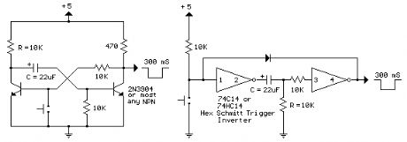
The monostable flip flop, sometimes called a 'one shot' is used to produce a single pulse each time it is triggered. It can be used to debounce a mechanical switch so that only one rising and one falling edge occurs for each switch closure, or to produce a delay for timing applications. In the discrete circuit, the left transistor normally conducts while the right side is turned off. Pressing the switch grounds the base of the conducting transistor causing it to turn off which causes the collector voltage to rise. As the collector voltage rises, the capacitor begins to charge through the base of the opposite transistor, causing it to switch on and produce a low state at the output. The low output state holds the left transistor off until the capacitor current falls below what is needed to keep the output stage saturated. When the output side begins to turn off, the rising voltage causes the left transistor to return to it's conducting state which lowers the voltage at it's collector and causes the capacitor to discharge through the 10K resistor (emitter to base). The circuit then remains in a stable state until the next input. The one shot circuit on the right employs two logic inverters which are connected by the timing capacitor. When the switch is closed or the input goes negative, the capacitor will charge through the resistor generating an initial high level at the input to the second inverter which produces a low output state. The low output state is connected back to the input through a diode which maintains a low input after the switch has opened until the voltage falls below 1/2 Vcc at pin 3 at which time the output and input return to a high state. The capacitor then discharges through the resistor (R) and the circuit remains in a stable state until the next input arrives. The 10K resistor in series with the inverter input (pin 3) reduces the discharge current through the input protection diodes. This resistor may not be needed with smaller capacitor values.
Note: These circuits are not re-triggerable and the output duration will be shorter than normal if the circuit is triggered before the timing capacitors have discharged which requires about the same amount of time as the output. For re-triggerable circuits, the 555 timer, or the 74123 (TTL), or the 74HC123 (CMOS) circuits can be used. (View)
View full Circuit Diagram | Comments | Reading(1440)
CMOS Toggle Flip Flop Using Laser Pointer
Published:2012/10/23 20:18:00 Author:muriel | Keyword: CMOS , Toggle , Flip Flop , Laser Pointer
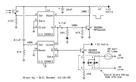
The circuit below is similar to the one above but can be used with a laser pointer to toggle the relay rather than a push button. The IR photo transistor Q1 (Radio Shack 276-145A) or similar is connected to the set input (pin 6). The photo transistor should be shielded from direct light so that the voltage at the set input (pin 6) is less than 1 volt under ambient conditions and moves to more than 10 volts when illuminated by the laser pointer or other light source. The reset time is about a half second using a 4.7uF cap which prevents the circuit from toggling more than once during a half second interval. The 10K resistor and diode provide a faster discharge path for the 4.7uF cap so the circuit can be retoggled in less than 1 second. The 3K resistor in series with the photo transistor may need be adjusted for best performance. The relay shown is a solid state variety to be used with lights or other resistive loads at less than 3 amps. A mechanical relay can also be used as shown in circuit above. (View)
View full Circuit Diagram | Comments | Reading(1055)
CMOS Toggle Flip Flop Using Push Button
Published:2012/10/23 20:17:00 Author:muriel | Keyword: CMOS , Toggle , Flip Flop, Push Button
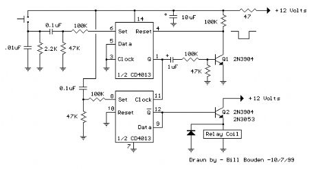
The circuit below uses a CMOS dual D flip flop (CD4013) to toggle a relay or other load with a momentary push button. Several push buttons can be wired in parallel to control the relay from multiple locations.
A high level from the push button is coupled to the set line through a small (0.1uF) capacitor. The high level from the Q output is inverted by the upper transistor and supplies a low reset level to the reset line for about 400 mS, after which time the reset line returns to a high state and resets the flip flop. The lower flip flop section is configured for toggle operation and changes state on the rising edge of the clock line or at the same time as the upper flip flop moves to the set condition. The switch is debounced due to the short duration of the set signal relative to the long duration before the circuit is reset. The Q or Qbar outputs will only supply about 2 mA of current, so a buffer transistor or power MOSFET is needed to drive a relay coil, or lamp, or other load. A 2N3904 or most any small signal NPN transistor can be used for relay coil resistances of 250 ohms or more. A 2N3053 or medium power (500 mA) transistor should be used for coil resistances below 250 ohms. The 47 ohm resistor and 10uF capacitor serve to decouple the circuit from the power supply and filter out any short duration noise signals that may be present. The RC network (.1/47K) at the SET line (pin 8) serves as a power-on reset to ensure the relay is denergized when circuit power is first applied. The reset idea was suggested by Terry Pinnell who used the circuit to control a shed light from multiple locations. (View)
View full Circuit Diagram | Comments | Reading(1213)
Single MOSFET Relay Toggle Circuit
Published:2012/10/23 20:16:00 Author:muriel | Keyword: Single MOSFET, Relay , Toggle Circuit
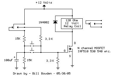
This circuit is similar to the one above, but uses a N channel mosfet such as IRF530, 540, 640, etc. in place of the NPN transistor. Smaller mosfets could be used, but I don't know the part numbers. I tested the circuit with a IRF640, IRFZ44, IRFZ34 and REP50N06.
The circuit has the same three advantages, it requires only a few parts, always comes up with the relay deactivated, and doesn't need any switch debouncing.
In operation, when the relay is deactivated, the 100uF capacitor will charge to 6 volts. When the button is pressed, the capacitor will apply 6 volts to the MOSFET gate turning it on. The capacitor voltage (and gate voltage) will fall from 6 to 3 volts in about 200 mS which should be enough time for the relay contacts to move. For very slow relays, a larger capacitor may be needed.
When the relay energizes, the contacts will apply 12 volts to the 3.3K resistor producing 6 volts at the gate, which will keep the relay energized indefinetly. The capacitor will now discharge to zero since the +12 relay contact is no longer connected to the 15K resistor.
When the button is again pressed, the capacitor will apply zero volts to the gate turning off the relay. There should be no problem holding down the button causing the relay to re-engage since the gate voltage will be only about 1.8 volts when the button is held down and the mosfet requires about 3.5 volts or more to start conducting. But you do need to wait about 1 second or longer between button presses, so the capacitor has time to charge or discharge. Two push buttons are shown, but you could have several more in parallel to control the relay from several different locations. (View)
View full Circuit Diagram | Comments | Reading(1903)
Single Transistor Relay Toggle Circuit
Published:2012/10/23 20:15:00 Author:muriel | Keyword: Single Transistor , Relay , Toggle Circuit

The circuit below requires a double pole, double throw relay in conjunction with a single transistor to allow toggling the relay with a momentary push button. One set of relay contacts is used to control the load, while the other is used to provide feedback to keep the relay activated or deactivated. Several push buttons can be wired in parallel to allow toggling the relay from different locations.
In the deactivated state, the relay contacts are arranged so the 1000 uF capacitor will charge to about 2.7 volts. When the switch is closed, the capacitor voltage is applied to the transistor base through a 560 resistor causing the transistor to turn on and activate the relay. In the activated state, the relay contacts are arranged so the 3.3K resistor and 560 ohm resistor provide a continous current to the transistor base maintaining the activated state. While in the activated state, the capacitor is allowed to discharge to zero through the 1K resistor. When the switch is again closed, the capacitor will cause the transistor base to move toward ground deactivating the relay.
The circuit has three distinct advantages, it requires only a few parts, always comes up with the relay deactivated, and doesn't need any switch debouncing. However since the capacitor will begin charging as soon as the button is depressed, the button cannot remain depressed too long to avoid re-engaging the relay. This problem can be minimized with an additional resistor connected from the transistor base to ground so that the base voltage is close to 0.7 volts with the button depressed and the transistor is biased in the linear region. With the button held down, the relay coil voltage should be somewhere between the pull in and drop out voltages so that the relay will maintain the last toggled state. This worked out to about 820 ohms for the circuit I built using a 12 volt, 120 ohm relay coil and 2N3053 transistor. Temperature changes will effect the situation but the operation is still greatly improved. I heated the transistor with a hair dryer and found that the relay will re-engage with the button held down for approximately 1 second, but this is not much of a problem under normal operation. (View)
View full Circuit Diagram | Comments | Reading(1617)
Relay Toggle Circuit Using a 556 Timer
Published:2012/10/23 20:15:00 Author:muriel | Keyword: Relay Toggle Circuit, 556 Timer
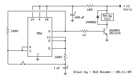
This toggle circuit operates by using a couple 555 timers wired as inverters. Pins 2 and 6 are the threshold and trigger inputs to the first timer and pin 5 is the output. The output at pin 5 will always be the inverse of the input at pins 2 and 6. Likewise, the output at pin 9 of the second timer will always be the inverse of the input at pins 8 and 12. A 100K resistor connects the output of one inverter to the input of the other so the state of one will be the opposite of the other.
In operation, the 1uF capacitor will charge to whatever voltage is present at the output on pin 5. When the button is pressed, the capacitor voltage will be applied to the input of the other timer which will reverse the state of both timers and toggle the relay, either on or off.
To follow it more closely, assume the output at pin 5 is +12 volts and the second output at pin 9 is zero volts. The 1uF cap will be charged to 12 volts. When the button is pressed, the cap will apply +12 to the inputs at pin 2 and 6 which will cause the output at pin 9 to go to zero, turning off the relay. When the button is released, the cap will discharge to zero, since the voltage at pin 5 is now zero. When the button is again pressed, the capacitor will apply zero to pins 2 and 6 causing the output at pin 9 to switch positive and engage the relay, and the cycle repeats.
The advantage of this circuit is the large hystersis range on the inputs. The button can be held closed indefinetly without upsetting the state of the outputs since the input voltage will be 1/2 the supply due to the equal value 100K resistors. The switching points are 1/3 and 2/3 of the supply so that a voltage of 50% has no effect. The circuit will also toggle very fast and needs no switch debouncing. One disadvantage is that it may turn on with the relay either engaged or disengaged. To solve that problem, you could use a resistor in series with one of the reset lines (4 or 10) and add a capacitor from the reset line to ground.
The 100 ohm resistor and 100uF capacitor serve to filter noise on the supply line if the circuit is used in a automotive application. They may not be necessary. The circuit may work well without those parts.
(View)
View full Circuit Diagram | Comments | Reading(2940)
Relay Toggle Circuit Using a 555 Timer
Published:2012/10/23 20:14:00 Author:muriel | Keyword: Relay Toggle Circuit, 555 Timer
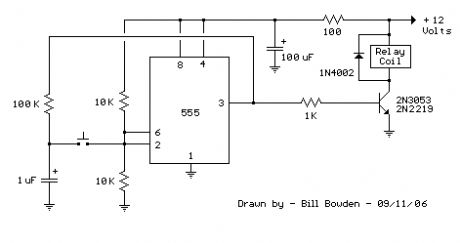
This 555 timer circuit below toggles a relay when a button is pressed. Pins 2 and 6, the threshold and trigger inputs, are held at 1/2 the supply voltage by the two 10K resistors. When the output is high, the capacitor charges through the 100K resistor, and discharges when the output is low. When the button is pressed, the capacitor voltage is applied to pins 2 and 6 which causes the output to change to the opposite state. When the button is released, the capacitor will charge or discharge to the new level at the output (pin 3). The parts are not critical, the resistors can be somewhat higher or lower, but the 2 resistors at pins 2 and 6 should be equal values, and the resistor connected to the cap should be 10 times greater or more.
Advantages of this circuit are the large hystersis range at the input which avoids false triggering, and only a few parts are needed for construction. One disadvantage is the relay may be engaged when power is first applied. To solve this problem, you could tie the reset line (pin 4) to another resistor/capacitor combination with the capacitor at ground and the resistor at the +V point. This will cause pin 4 to be held near ground for a short period which will reset the output when power is applied.
The 100 ohm resistor and 100uF capacitor serve to filter noise on the supply line if the circuit is used in a automotive application. They may not be necessary. The circuit may work well without those parts. (View)
View full Circuit Diagram | Comments | Reading(1869)
High Current MOSFET Toggle Switch with Debounced Push Button.
Published:2012/10/22 22:15:00 Author:muriel | Keyword: High Current MOSFET , Toggle Switch , Debounced Push Button
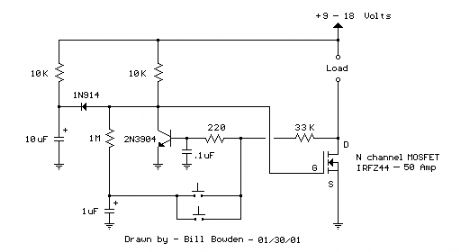
This circuit was adapted from the Toggle Switch Debounced Pushbutton by John Lundgren. It is useful where the load needs to be switched on from one location and switched off from another. Any number of momentary (N/O) switches or push buttons can be connected in parallel.
The combination (10K, 10uF and diode) on the left side of the schematic insures the circuit powers up with the load turned off and the NPN transistor conducting. These components can be omitted if the initial power-on condition is not an issue.
When a switch is closed, the 1uF cap voltage is connected to the junction of the 220 ohm and 33K resistors causing the circuit to change state. When the switch is opened, the cap charges or discharges to the new level through the 1M resistor, and the circuit is ready to toggle again in about 1 second. It takes a little time for the cap to move to the new level, either +V or ground.
The (0.1uF) capacitor at the transistor base was added to supress noise that might cause false triggering if the switches are located far away from the circuit. The circuit was tested using a 12 volt, 25 watt automotive lamp, and IRFZ44. Other MOSFETs can probably be used.
(View)
View full Circuit Diagram | Comments | Reading(1708)
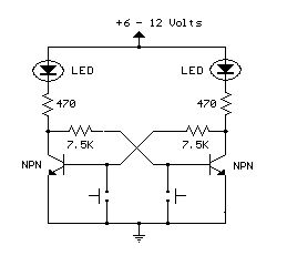
Bistable Flip Flop
Published:2012/10/22 22:09:00 Author:muriel | Keyword: Bistable, Flip Flop
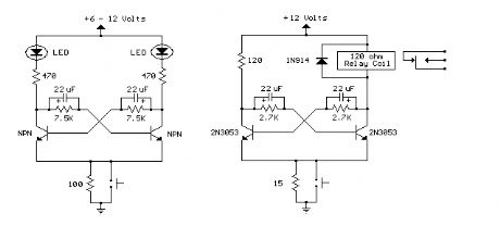
Here are two examples of bistable flip flops which can be toggled between states with a single push button. When the button is pressed, the capacitor connected to the base of the conducting transistor will charge to a slightly higher voltage. When the button is released, the same capacitor will discharge back to the previous voltage causing the transistor to turn off. The rising voltage at the collector of the transistor that is turning off causes the opposite transistor to turn on and the circuit remains in a stable state until the next time the button is pressed and released. Note that in the LED circuit, the base current from the conducting transistor flows through the LED that should be off, causing it to illuminate dimly. The base current is around 1 mA and adding a 1K resistor in parallel with the LED will reduce the voltage to about 1 volt which should be low enough to ensure the LED turns completely off.
(View)
View full Circuit Diagram | Comments | Reading(1136)
Set/Reset Flip Flop
Published:2012/10/22 22:08:00 Author:muriel | Keyword: Set/Reset, Flip Flop
This is an example of a set/reset flip flop using discrete components. When power is applied, only one of the transistors will conduct causing the other to remain off. The conducting transistor can be turned off by grounding it's base through the push button which causes the collector voltage to rise and turn on the opposite transistor. (View)
View full Circuit Diagram | Comments | Reading(1489)
Experiments with Detector Diodes
Published:2012/10/22 22:07:00 Author:muriel | Keyword: Experiments, Detector Diodes
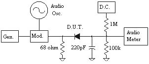
When building crystal radios or other simple receivers, the experimenter often wonders about the relative performance of the different diodes in the junk box. Here are the results of several experiments using the typical types available to the hobbyist. The source is a low impedance and the load is a fairly high impedance. A particular diode will behave differently with different impedance levels but for low received signal levels these measurements are fairly predictive of the relative performance in most circuits. The diode types include germanium, silicon, Schottky, and even a light-emitting diode! The test setup uses an accurate RF synthesizer, a homemade AM pin diode modulator driven by an audio generator, a simple test fixture, a DC power supply for adding bias current, and a sensitive audio voltmeter. The setup shown below was used to test the diodes at several frequencies with a low modulation index (about 20%) and the near optimum bias current was determined by varying the DC supply. (View)
View full Circuit Diagram | Comments | Reading(1162)
Simple Two-Transistor Radio
Published:2012/10/22 22:07:00 Author:muriel | Keyword: Simple, Two-Transistor, Radio
Here is a simple radio that was designed to minimize unusual parts; there isn't even a detector diode! The sensitivity isn't as high as the one-transistor reflex but the simplicity is attractive. Strong stations will provide plenty of volume into a crystal earphone or an external amplifier. The AM Loopstick was purchased on eBay but the enterprising experimenter can swipe one from the interior of a cheap radio. If the loopstick has more than one winding, use the one with the most turns. Wind 3 or 4 turns near one end of the winding as seen in the photo. The tuning capacitor in the prototype is from an old radio and the little plastic dial was cut down such that it just fit into the back of a black pointer knob. The fit was tight so no glue was needed. All of the sections of the capacitor were connected in parallel to get the most capacitance for this loopstick.
All the other parts are common. The transistors can be just about any small-signal type. The prototype uses the metal can 2N2222, primarily for looks. Some transistors may have too much high frequency gain; if the circuit squeals, try adding a small resistor in the emitter of the first transistor, maybe 47 ohms, the smaller the better as long as the circuit is stable. The large 47 uF could be smaller in most cases but the circuit can pick up hum if the wires are too long. Don't leave out the large capacitor across the battery, it provides needed low power supply impedance. (View)
View full Circuit Diagram | Comments | Reading(2746)
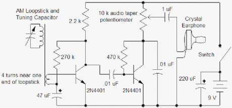
Very High Gain Crystal Earphone Amplifier
Published:2012/10/22 22:06:00 Author:muriel | Keyword: Very High Gain , Crystal Earphone, Amplifier
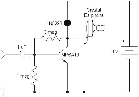
This simple, one-transistor amplifier provides a voltage gain over 1000 (60 dB) for driving a high impedance ceramic (crystal) earphone. The high gain is achieved by replacing the traditional collector resistor with an unusual constant-current diode that supplies 1/2 mA yet exhibits a very high resistance to the audio. This amplifier will give excellent battery life, drawing only 500 uA. (View)
View full Circuit Diagram | Comments | Reading(1642)
Crystal Radio RF Amplifiers
Published:2012/10/22 22:05:00 Author:muriel | Keyword: Crystal Radio, RF Amplifiers
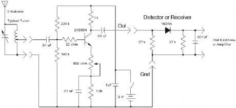
One of the best places to add a transistor to a simple crystal radio is at the front end in the form of an RF amplifier. The circuit below is a simple but effective amplifier which will give surprising performance improvement. This amplifier can exhibit negative resistance for low settings of the 500 ohm pot which results in extra gain or even oscillation. So, the circuit can actually be considered to be a regenerative receiver with an external detector. The sensitivity is so high that no cold water pipe ground is needed and the antenna is short. (View)
View full Circuit Diagram | Comments | Reading(2412)
Crystal Radio Audio Amplifiers
Published:2012/10/22 22:05:00 Author:muriel | Keyword: Crystal Radio, Audio Amplifiers
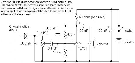
Here is a simple audio amplifier using a TL431 shunt regulator. The amplifier will provide room-filling volume from an ordinary crystal radio outfitted with a long-wire antenna and good ground. The circuitry is similar in complexity to a simple one-transistor radio but the performance is far superior. The TL431 is available in a TO-92 package and it looks like an ordinary transistor so your hobbyist friends will be impressed by the volume you are getting with only one transistor! The amplifier may be used for other projects, too. Higher impedance headphones and speakers may also be used. An earphone from an old telephone will give ear-splitting volume and great sensitivity! The 68 ohm resistor may be increased to several hundred ohms when using high impedance earphones to save battery power. (View)
View full Circuit Diagram | Comments | Reading(1572)
One Transistor Amplifier/Detector
Published:2012/10/22 22:04:00 Author:muriel | Keyword: One Transistor , Amplifier, Detector
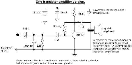
An amplifier may be added to boost the audio level as shown below. The current consumption of this amplifier is quite low and a power switch is not included. Disconnect the battery when the receiver is stored for long periods. (View)
View full Circuit Diagram | Comments | Reading(1988)
Simple Crystal Radio
Published:2012/10/22 22:03:00 Author:muriel | Keyword: Simple Crystal Radio
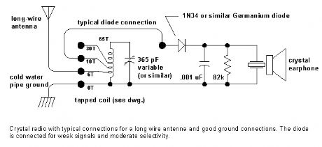
The crystal radio gets its name from the galena crystal (lead sulfide) used to rectify the signals. A cat's whisker wire contact was moved about the surface of the crystal until a diode junction was formed. The 1N34A germanium diode is the modern substitute for galena and most other germanium small-signal diodes will also work well. Silicon diodes are not a good choice because their much higher barrier potential requires larger signals for efficient rectification. Certain silicon Schottky diodes with low barrier potential will work well but most small-signal Schottky diodes will not perform as well as a garden-variety germanium diode. (View)
View full Circuit Diagram | Comments | Reading(0)
Varying brightness AC lamp
Published:2012/10/22 21:59:00 Author:muriel | Keyword: Varying brightness, AC lamp
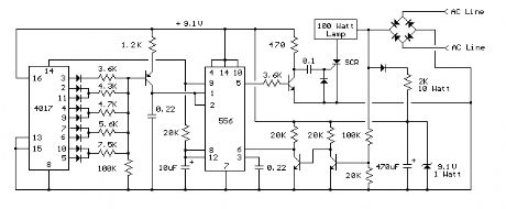
In this circuit, an SCR is used to slowly vary the intensity of a 120 volt light bulb by controlling the time that the AC line voltage is applied to the lamp during each half cycle. Caution: The circuit is directly connected to the AC power line and should be placed inside an enclosure that will prevent direct contact with any of the components. To avoid electrical shock, do not touch any part of the circuit while it is connected to the AC power line. A 2K, 10 watt power resistor is used to drop the line voltage down to 9 volts DC. This resistor will dissipate about 7 watts and needs some ventilation. Operation: A couple NPN transistors are used to detect the beginning of each half cycle and trigger a delay timer which in turn triggers the SCR at the end of the delay time. The delay time is established by a current source which is controlled by a 4017 decade counter. The first count (pin 3) sets the current to a minimum which corresponds to about 7 milliseconds of delay, or most of the half cycle time so that the lamp is almost off. Full brightness is obtained on the sixth count (pin 1) which is not connected so that the current will be maximum and provide a minimum delay and trigger the SCR near the beginning of the cycle. The remaining 8 counts increment the brightness 4 steps up and 4 steps down between maximum and minimum. Each step up or down provides about twice or half the power, so that the intensity appears to change linearly. The brightness of each step can be adjusted with the 4 resistors (4.3K, 4.7K, 5.6K, 7.5K) connected to the counter outputs.
The circuit has been built by Don Warkentien (WODEW) who suggsted adding a small 47uF capacitor from ground to the junction of the current source transistor (PNP) to reduce the digital stepping effect so the lamp will brighten and fade in a smoother fashion. The value of this capacitor will depend on the 4017 counting rate, a faster rate would require a smaller capacitor. (View)
View full Circuit Diagram | Comments | Reading(1813)
| Pages:295/2234 At 20281282283284285286287288289290291292293294295296297298299300Under 20 |
Circuit Categories
power supply circuit
Amplifier Circuit
Basic Circuit
LED and Light Circuit
Sensor Circuit
Signal Processing
Electrical Equipment Circuit
Control Circuit
Remote Control Circuit
A/D-D/A Converter Circuit
Audio Circuit
Measuring and Test Circuit
Communication Circuit
Computer-Related Circuit
555 Circuit
Automotive Circuit
Repairing Circuit