
Circuit Diagram
Index 298
60 Light Sequencer using a Matrix
Published:2012/10/22 1:14:00 Author:muriel | Keyword: 60 Light Sequencer, Matrix
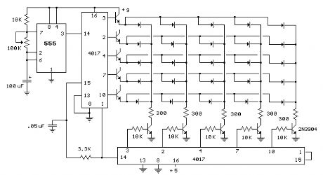
The circuit below illustrates using a 10x10 matrix to sequence up to 100 LEDs with just three ICs and 20 transistors. The two 4017 decade counters control the 10 rows and 10 columns so that one LED is selected depending on the output of the decade counters.
The LED circuit is drawn showing 25 LEDs and 10 transistors but can be expanded up to a 100 by using sucessive stages of the 4017 counters.
For example, to expand the circuit to 60 LEDs for displaying minutes or seconds of a clock, the rows counter could be reset from pin 12 (carry out) rather than pin 1 as shown, and the columns counter will be reset from pin 5 rather than pin 1 as shown. And then add transistors to pins 1,5,6,9,and 11 of the rows counter and pin 1 of the columns counter. Take a look at the 10 Stage LED Sequencer for a listing of all the connections of the 4017 decade counter. (View)
View full Circuit Diagram | Comments | Reading(2880)
50 Hertz LED Clock Timebase
Published:2012/10/22 1:13:00 Author:muriel | Keyword: 50 Hertz , LED Clock , Timebase
View full Circuit Diagram | Comments | Reading(1182)
72 LED Clock
Published:2012/10/22 1:11:00 Author:muriel | Keyword: 72 , LED Clock
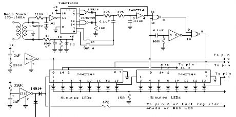
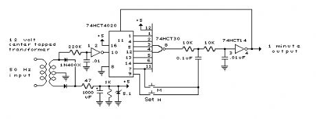
In the circuit below, 60 individual LEDs are used to indicate the minutes of a clock and 12 LEDs indicate hours. The power supply and time base circuitry is the same as described in the 28 LED clock circuit above. The minutes section of the clock is comprised of eight 74HCT164 shift registers cascaded so that a single bit can be recirculated through the 60 stages indicating the appropriate minute of the hour. Only two of the minutes shift registers are shown connected to 16 LEDs. Pin 13 of each register connects to pin 1 of the next for 7 registers. Pin 6 of the 8th register should connect back to pin 1 of the first register using the 47K resistor. Pins 2,9,8, 14 and 7 of all 8 minutes registers (74HC164) should be connected in parallel (pin 8 to pin 8, pin 9 to pin 9, etc.). The hours section contains two 8 bit shift registers and works the same way as the minutes to display 1 of 12 hours. Pin 9 of all 74HCT164s (hours and minutes) should be connected together. For 50 Hertz operation, the time base section of the circuit can be modified as shown in the lower drawing labeled 50 Hertz LED Clock Time Base . You will need an extra IC (74HC30) to do this since it requires decoding 7 bits of the counter instead of 4. The two dual input NAND gates (1/2 74HC00) that are not used in the 50 Hertz modification should have their inputs connected to ground.
When power is applied, a single 1 bit is loaded into the first stage of both the minutes and hours registers. To accomplish this, a momentary low reset signal is sent to all the registers (at pin 9) and also a NAND gate to lock out any clock transitions at pin 8 of the minutes registers. At the same time, a high level is applied to the data input lines of both minutes and hours registers at pin 1. A single positive going clock pulse (at pin 8) is generated at the end of the reset signal which loads a high level into the first stage of the minutes register. The rising edge of first stage output at pin 3 advances the hours (at pin 8) and a single bit is also loaded into the hours register. Power should remain off for about 3 seconds or more before being re-applied to allow the filter and timing capacitors to discharge. A 1K bleeder resistor is used across the 1000uF filter capacitor to discharge it in about 3 seconds. The timing diagram illustrates the power-on sequence where T1 is the time power is applied and beginning of the reset signal, T2 is the end of the reset signal, T3 is the clock signal to move a high level at pin 1 into the first register, T4 is the end of the data signal. The time delay from T2 to T3 is exaggerated in the drawing and is actually a very short time of just the propagation delay through the inverter and gate.
Two momentary push buttons can be used to set the correct time. The button labeled M will increment the minutes slowly and the one labled H much faster so that the hours increment slowly. The hours should be set first, followed by minutes. (View)
View full Circuit Diagram | Comments | Reading(1820)
28 LED Clock Timer
Published:2012/10/22 1:09:00 Author:muriel | Keyword: 28 LED, Clock Timer
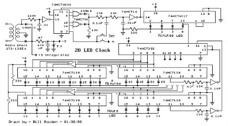
This is a programmable clock timer circuit that uses individual LEDs to indicate hours and minutes. 12 LEDs can be arranged in a circle to represent the 12 hours of a clock face and an additional 12 LEDs can be arranged in an outer circle to indicate 5 minute intervals within the hour. 4 additional LEDs are used to indicate 1 to 4 minutes of time within each 5 minute interval. The circuit is powered from a small 12.6 volt center tapped line transformer and the 60 cycle line frequency is used for the time base. The transformer is connected in a full wave, center tapped configuration which produces about 8.5 volts unregulated DC. A 47 ohm resistor and 5.1 volt, 1 watt zener regulate the supply for the 74HCT circuits. A 14 stage 74HCT4020 binary counter and two NAND gates are used to divide the line frequency by 3600 producing a one minute pulse which is used to reset the counter and advance the 4017 decade counter. The decade counter counts the minutes from 0 to 4 and resets on the fifth count or every 5 minutes which advances one section of a dual 4 bit binary counter (74HCT393). The 4 bits of this counter are then decoded into one of 12 outputs by two 74HCT138 (3 line to 8 line) decoder circuits. The most significant bit is used in conjunction with an inverter to select the appropriate decoder. During the first eight counts, the low state of the MSB is inverted to supply a high level to enable the decoder that drives the first 8 LEDs. During counts 9 to 12, the MSB will be high and will select the decoder that drives the remaining 4 LEDs while disabling the other decoder. The decoded outputs are low when selected and the 12 LEDs are connected common anode with a 330 ohm current limiting resistor to the +5 volt supply. The 5th output of the second decoder (pin 11) is used to reset the binary counter so that it counts to 11 and then resets to zero on the 12th count. A high reset level is required for the 393 counters, so the low output from the last decoder stage (pin 11) is inverted with one section of a 74HCT14 hex Schmitt trigger inverter circuit. A 10K resistor and 0.1uF cap are used to extend the reset time, ensuring the counter receives a reset signal which is much longer than the minimum time required. The reset signal is also connected to the clock input (pin 13) of the second 4 bit counter (1/2 74HCT393) which advances the hour LEDs and resets on the 12th hour in a similar manner. Setting the correct time is accomplished with two manual push buttons which feed the Q4 stage (pin 7) of the 4020 counter to the minute and hour reset circuits which advance the counters at 3.75 counts per second. A slower rate can be obtained by using the Q5 or Q6 stages. For test purposes, you can use Q1 (pin 9) which will advance the minutes at 30 per second. The time interval circuit (shown below the clock) consists of a SET/RESET flipflop made from the two remaining NAND gates (74HCT00). The desired time interval is programmed by connecting the anodes of the six diodes labeled start, stop and AM/PM to the appropriate decoder outputs. For example, to turn the relay on at 7:05AM and turn it off at 8:05AM, you would connect one of the diodes from the start section to the cathode of the LED that represents 7 hours, the second diode to the LED cathode that represents 5 minutes and the third diode to the AM line of the CD4013. The stop time is programmed in the same manner. Two additional push buttons are used to manually open and close the relay. The low start and stop signals at the common cathode connections are capacitively coupled to the NAND gates so that the manual push buttons can override the 5 minute time duration. That way, you can immediately reset the relay without waiting 5 minutes for the start signal to go away. The two power supply rectifier diodes are 1N400X variety and the switching diodes are 1N914 or 4148s but any general purpose diodes can be used. 0.1 uF caps (not shown on schematic) may be needed near the power pins of each IC. All parts should be available from Radio Shack with the exception of the 74HCT4017 decade counter which I didn't see listed. You can use either 74HC or 74HCT parts, the only difference between the two is that the input switching levels of the HCT devices are compatible with worst case TTL logic outputs. The HC device inputs are set at 50% of Vcc, so they may not work when driven from marginal TTL logic outputs. You can use a regular 4017 in place of the 74HCT4017 but the output current will much lower (less than 1 mA) and 4 additional transistors will be required to drive the LEDs. Without the buffer transistors, you can use a 10K resistor in place of the 330 and the LEDs will be visible, but very dim. Using the 4017 to drive LEDs with transistor buffers is shown in the 10 Channel LED Sequencer at the top of this page. (View)
View full Circuit Diagram | Comments | Reading(1032)
Automobile Interior Lights Fader
Published:2012/10/22 1:08:00 Author:muriel | Keyword: Automobile Interior, Lights Fader
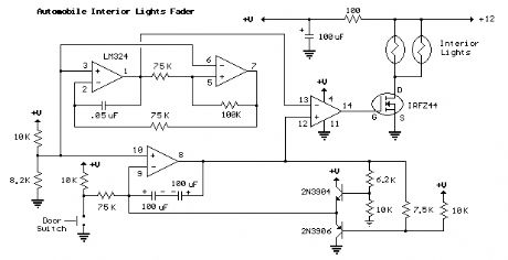
The circuit is based around the LM324 low power opamp which draws around 3mA of current, so it won't bother the battery if left connected for extended periods.
The top two opamps (pins 1,2,3 and 5,6,7) form a triangle wave oscillator running at about 700Hz while the lower opamp (pins 8,9,10) produces a linear, 5 second ramp, that moves up or down depending on the position of the door switch. The two transistors and associated resistors serve to limit the ramp voltage to slightly more and less than the upper and lower limits of the triangle waveform. These two signals (700 hZ. triangle wave and 5 second ramp) are applied to the inputs of the 4th opamp (pins 12,13,14) that serves as a voltage comparator and generates a varying duty cycle square wave that controls the IRFZ44 MOSFET and lamp brightness. The 5 second fade time can be adjusted with the 75K resistor connected to the door switch. A larger value will increase the time and a smaller value will speed it up.
When the door switch is closed (car door open) the voltage on pin 8 slowly rises above the negative peaks of the triangle wave producing a short duty cycle output and a dim light. As the ramp moves farther positive, a greater percentage of the triangle wave will be lower than the ramp voltage producing a wider pulse and brighter light. This process continues until the ramp is 100% above the positive peaks of the triangle wave and the output is maximum. When the door switch is open, the reverse action takes place and the lamps slowly fade out.
The IRFZ44 shouldn't require a heat sink if the total load is 50 watts or less but the temperature of the MOSFET should be monitored to insure it doesn't overheat. The on-state resistance is only 0.028 ohms so that 4 amps of current (48 watts) is only around 100mW. For larger loads, a small heat sink can be added to keep the MOSFET cool. (View)
View full Circuit Diagram | Comments | Reading(1460)
Fading Red Eyes
Published:2012/10/22 1:07:00 Author:muriel | Keyword: Fading, Red Eyes
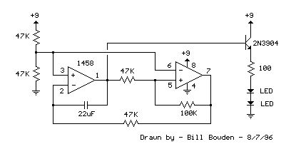
This circuit is used to slowly illuminate and fade a pair of redLEDs (light emitting diodes). The fading LEDs could be installedas 'eyes' in a small pumpkin or skull as a Halloween attraction,or mounted in a Christmas tree ornament. Or, they might be usedas a fancy power indicator for your computer, microwave oven,stereo system, TV, or other appliance.In operation, a linear 3 volt (peak to peak) ramping waveform isgenerated at pin 1 of the LM1458 IC and buffered with an emitter followertransistor stage. The 22uF capacitor and 47K resistor connected topin 2 establish the frequency which is about 0.5 Hz. You can make therate adjustable by using a 100K potentiometer in place of the 47Kresistor at pin 2.The circuit consists of two operational amplifiers (opamps),one producing a slow rising and falling voltage from about 3 volts to6 volts, and the other (on the right) is used as a voltage comparator,the output of which supplies a alternating voltage switching between2 and 7 volts to charge and discharge the capacitor with a constantcurrent. (View)
View full Circuit Diagram | Comments | Reading(2008)
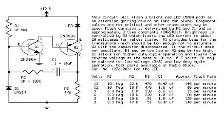
Two Transistor LED Flasher
Published:2012/10/22 1:06:00 Author:muriel | Keyword: Two Transistor, LED Flasher
View full Circuit Diagram | Comments | Reading(1474)
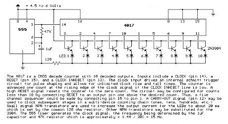
18 Stage LED Sequencer
Published:2012/10/22 1:05:00 Author:muriel | Keyword: 18 Stage, LED Sequencer
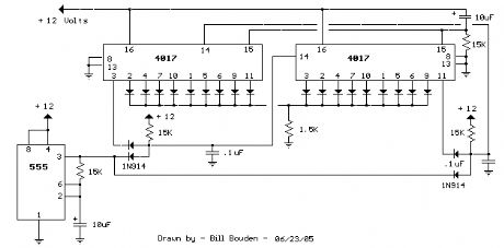
The question sometimes comes up of how to cascade 4017 decade counters for more than 10 sequencial stages. The LED sequencer below shows a possible solution using a few extra parts.
When power is applied, the 15K resistor and 10uF cap at pin 15 will reset the counters to the zero count where pin 3 is at +12 and all other outputs are at zero. The 2 diodes (1n914) and 15 resistor form a AND gate so the clock pulse will be passed to the right side counter when the sequence starts. When the right counter reaches the 10th count, pin 11 will move high enabling the AND gate on the right to pass the clock pulse to the left side counter. As the left side counter advances, pin 3 will be low so that clock pulses cannot advance the right counter. When the left counter turns over and pin 3 again moves high, the sequence will repeat. Thus we get 18 total counts, 9 from the first counter, and 9 from the second.
Note that the 4017 counter will not deliver much current, and so the LED current is set to about 6mA using a 1.5K resistor in series. For more current, you could use transistors on each output as shown in the drawing above, (10 Channel LED Sequencer). But some of the newer bright LEDs are fairly bright at 6mA. (View)
View full Circuit Diagram | Comments | Reading(2705)
10 Channel LED Sequencer
Published:2012/10/22 1:04:00 Author:muriel | Keyword: 10 Channel, LED Sequencer
View full Circuit Diagram | Comments | Reading(1950)
Expandable 16 Stage LED Sequencer
Published:2012/10/22 1:03:00 Author:muriel | Keyword: Expandable , 16 Stage, LED Sequencer
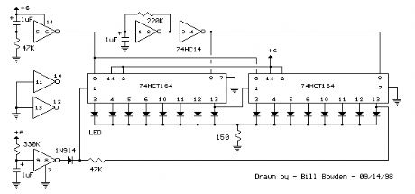
The circuit below uses a hex Schmitt Trigger inverter (74HC14) and two 8 bit Serial-In/Parallel-Out shift registers (74HCT164 or 74HC164) to sequence 16 LEDs. The circuit can be expanded to greater lengths by cascading additional shift registers and connecting the 8th output (pin 13) to the data input (pin 1) of the succeeding stage. A Schmitt trigger oscillator (74HC14 pin 1 and 2) produces the clock signal for the shift registers, the rate being approximately 1/RC. Two additional Schmitt Trigger stages are used to reset and load the registers when power is turned on. Timing is not critical, however the output at pin 8 of the Schmitt Trigger must remain high during the first LOW to HIGH clock transition at pin 8 of the registers, and must return low before the second rising edge to load a single bit. If the clock rate is increased, the length of the signal at pin 9 of the Schmitt Trigger should be reduced proportionally to avoid loading more than one bit. The HCT devices will normally provide about 4 mA (source or sink) from each output but can supply greater currents (possibly 25 mA) if only one output is loaded. The common 150 ohm resistor restricts the current below 25 mA using a 6 volt power source. If the circuit is operated with two or more LEDs on at the same time, resistors may be needed in series with each LED to avoid exceeding the maximum total output current for each IC of 25 mA. For greater brightness, individual buffer transistors can be used as shown in the 10 stage LED sequencer on this same page. (View)
View full Circuit Diagram | Comments | Reading(2240)
Interfacing 5 volt CMOS to 12 volt/ 25 Watt Loads
Published:2012/10/22 1:03:00 Author:muriel | Keyword: Interfacing , 5 volt , CMOS to 12 volt/ 25 Watt, Loads
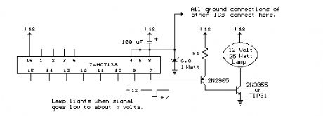
The circuit below is designed to be used with the bi-directional lamp sequencer shown above on this same page. Two additional transistors are used to increase the current from the 74HCT138 decoder to control 12 volt 25 watt lamps. A 6.8 volt/1 watt zener diode is used in series with the ground connection of all the CMOS ICs (74HC14, CD4516 and 74HC138s) so that the total voltage across the CMOS devices will be about 5.2 volts and the outputs will move from +12 to about +7 when selected. The 2N2905/PNP transistor stage is connected as an emitter follower which provides a high impedance to the decoder output and supplies about 80 mA of current to the base of the 2N3055 NPN power transistor which then supplies 2 or more amps to the 12 volt lamp. The voltage across the PNP transistor will be about 7 volts when it is turned on and the heat dissapation will be about 0.6 watts. That should't require a heat sink if several lamps are sequencing but it may get quite warm if the circuit is idle on a single output. The 2N3055 power transistor operates as a switch and drops very little voltage (less than 0.5) when conducting, and will not require a heat sink. Other transistors may be substituted such as the TIP29 or TIP31 for the 2N3055 and most any medium power (500mA) PNP for the 2N2905. (View)
View full Circuit Diagram | Comments | Reading(1015)
16 Stage Bi-Directional LED Sequencer
Published:2012/10/22 1:02:00 Author:muriel | Keyword: 16 Stage , Bi-Directional , LED Sequencer
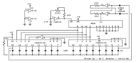
The bi-directional sequencer uses a 4 bit binary up/down counter (CD4516) and two 1 of 8 line decoders (74HC138 or 74HCT138) to generate the popular Night Rider display. A Schmitt Trigger oscillator provides the clock signal for the counter and the rate can be adjusted with the 500K pot. Two additional Schmitt Trigger inverters are used as a SET/RESET latch to control the counting direction (up or down). Be sure to use the 74HC14 and not the 74HCT14, the 74HCT14 may not work due to the low TTL input trigger level. When the highest count is reached (1111) the low output at pin 7 sets the latch so that the UP/DOWN input to the counter goes low and causes the counter to begin decrementing. When the lowest count is reached (0000) the latch is reset (high) so that the counter will begin incrementing on the next rising clock edge. The three lowest counter bits (Q0, Q1, Q2) are connected to both decoders in parallel and the highest bit Q3 is used to select the appropriate decoder. The circuit can be used to drive 12 volt/25 watt lamps with the addition of two transistors per lamp as shown below in the section below titled Interfacing 5 volt CMOS to 12 volt loads (View)
View full Circuit Diagram | Comments | Reading(1265)
Descrete Multistage Light Sequencer
Published:2012/10/22 1:01:00 Author:muriel | Keyword: Descrete Multistage , Light Sequencer
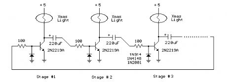
The drawing below illustrates a multistage light sequencer using descrete parts and no integrated circuits. The idea is not new and I hear a similar circuit was developed about 40 years ago using germanium transistors. The idea is to connect the lights so that as one turns off it causes the next to turn on, and so forth. This is accomplished with a large capacitor between each stage that charges when a stage turns off and supplies base current to the next transistor, thus turning it on. Any number of stages can be used and the drawing below illustrates 3 small Christmas lights running at about 5 volts and 200mA. The circuit may need to be manually started when power is applied. To start it, connect a momentary short across any one of the capacitors and then remove the short. You could use a manual push button to do this.
Detailed operation:
Assume the circuit doesn't start when power is applied amd all lights are off and all three capacitors are charged to about 5 volts. We connect a jumper across the 220uF capacitor on the left which discharges the capacitor and turns on the 2nd stage transistor and corresponding light. When the jumper is removed, the capacitor will start charging through the base of the stage 2 transistor and stage 1 light. This causes the stage 2 transistor to remain on while the capacitor continues to charge. At the same time, the capacitor connecting stage 2 and 3 will discharge through the 100 ohm resistor and diode and stage 2 transistor. When the capacitor charging current falls below what is needed to keep stage 2 turned on, the transistor and light will turn off causing the voltage at the collector of the stage 2 transistor to rise to 5 volts. Since the capacitor connecting stage 2 and 3 has discharged and the voltage rises at the collector of stage 2, the capacitor from stage 2 and 3 will charge causing the 3rd stage to turn on and the cycle repeats for sucessive stages 4,5,6,7.... and back to 1. The sequence rate is determined by the capacitor and resistor values (220uF and 100 ohms in this case), load current (200mA in this case), and current gain of the particular transistor used. This arrangement runs at about 120 complete cycles per minute for 3 lights, or about 167mS per light. Faster or slower rates can be obtained with different capacitor values. (View)
View full Circuit Diagram | Comments | Reading(1289)
1.5 volt dual LED flasher (runs one year)
Published:2012/10/22 1:01:00 Author:muriel | Keyword: 1.5 volt, dual LED , flasher, runs one year
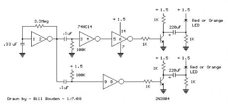
This 1.5 volt led fasher runs more than a year on a single 'd cell and alternately flashes 2 LEDs at about a 1 second rate. The circuit employs a 74HC14 CMOS hex inverter that will operate at very low voltages (less than 1 volt). One section is used as a squarewave oscillator (pins 1 and 2), while the others are wired to produce a short 10mS pulse on alternate edges of the square wave so the LEDs will alternate back and forth. The output sections each use a capacitor charge pump to increase the voltage for the LEDs. The circuit draws an average current of 800uA from the 'D' battery and the LED peak current is about 40mA with a fresh battery and drops to about 10mA as the battery voltage falls to 1.1 volts. The capacity of a alkaline 'D' cell is about 12 amp hours with a cutoff voltage of 1.1 so the circuit should run about 12/.0008 = 15000 hours or maybe 625 days, but I haven't verified that yet. (View)
View full Circuit Diagram | Comments | Reading(1564)
Digital metal detector circuit diagram
Published:2012/10/18 22:42:00 Author:Ecco | Keyword: Digital metal detector
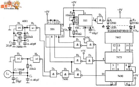
In the circuit, it uses 1MHz crystal X to generate a reference oscillation frequency, metal detector use L coil oscillator with the same nominal frequency, and NAND gate D6 will mix square wave reference signal produced by crystal oscillator and detection signal to produce a beat frequency signal circuit. 555 generates a approximately 500Hz frequency signal to drive the display 556 and NAND gate will merge the detection and display signals to add to 7490 and 7475 input ends, thereby driving the LED1 ~ LED10 emitting diodes.
(View)
View full Circuit Diagram | Comments | Reading(7904)
High-end current monitoring circuit diagram using HFP2
Published:2012/10/18 22:49:00 Author:Ecco | Keyword: High-end , current monitoring
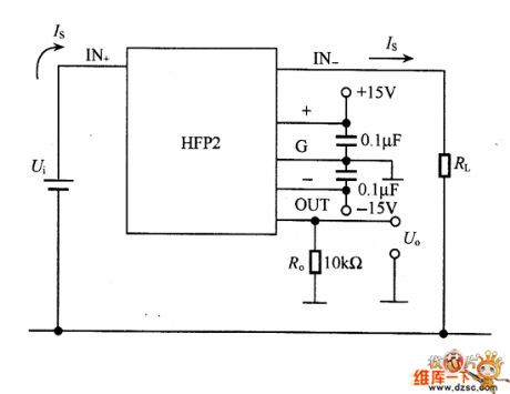
This is a high-end current monitoring circuit using DC transformer, and the working target is the same with Figure 8-9. HFP2 is a low offset voltage DC current transformer which can be easily mounted on the printed circuit board. The maximum voltage of the detected current is decided by the power between the input and output voltage of DC transformer, when the pressure reaches lkV above, the resistor Ro can not be used in principle, but the resistor is recommended by the manufacturer.
(View)
View full Circuit Diagram | Comments | Reading(1354)
AN7115 audio power amplifier circuit diagram
Published:2012/10/18 22:51:00 Author:Ecco | Keyword: audio power amplifier
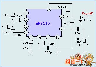
When Vvv = 9.0V , THD = 10% , RL = 8Ω, the output power of AN7114 can be up to 2.1W, the noise output is 3mV. Limiting parameters: Vcc = 13V, power dissipation (without heat sink ) is 1.2W and 2.25W with radiator. Operating temperature: -20 to 70 ℃. It is suitable for small, portable the closing tape recorders and audio equipment for power amplifier.
(View)
View full Circuit Diagram | Comments | Reading(2219)
Partial pressure biasing common-emitter amplifier circuit diagram
Published:2012/10/19 1:15:00 Author:Ecco | Keyword: Partial pressure , biasing , common-emitter amplifier
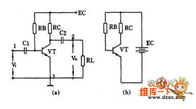
As shown in figure, the base voltage is obtained by rbl and rb2, so called partial pressure bias. The emitter adds resistor RE and capacitor CE, and CE is called AC bypass capacitor which can cause shorted circuit for AC, re has DC negative feedback influence.
(View)
View full Circuit Diagram | Comments | Reading(1113)
The voice recorder module hardware circuit
Published:2012/10/19 1:01:00 Author:Ecco | Keyword: voice recorder , module hardware
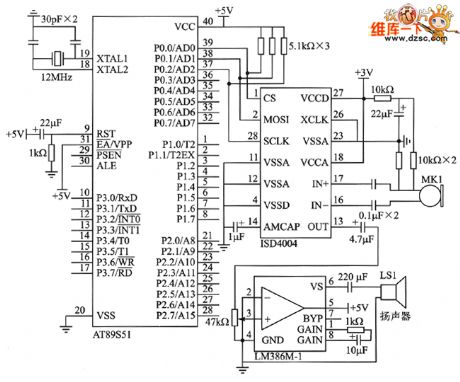
MK1 is a microphone for recording voice, and it can complete an ordinary live recording. In playback circuit, the output selects low voltage general purpose integrated power amplifier LM386M-1's typical application circuit as speaker LS1's driver circuit. In typical circuit, a 10μF bypass capacitor is connected between LM386M - 1's 1 feet and 8 feet to increase magnification with 200 times.
(View)
View full Circuit Diagram | Comments | Reading(1718)
High Current Regulated Supply
Published:2012/10/19 0:57:00 Author:muriel | Keyword: High Current, Regulated Supply
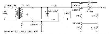
The high current regulator below uses an additional winding or a separate transformer to supply power for the LM317 regulator so that the pass transistors can operate closer to saturation and improve efficiency. For good efficiency the voltage at the collectors of the two parallel 2N3055 pass transistors should be close to the output voltage. The LM317 requires a couple extra volts on the input side, plus the emitter/base drop of the 3055s, plus whatever is lost across the (0.1 ohm) equalizing resistors (1volt at 10 amps), so a separate transformer and rectifier/filter circuit is used that is a few volts higher than the output voltage. The LM317 will provide over 1 amp of current to drive the bases of the pass transistors and assumming a gain of 10 the combination should deliver 15 amps or more. The LM317 always operates with a voltage difference of 1.2 between the output terminal and adjustment terminal and requires a minimum load of 10mA, so a 75 ohm resistor was chosen which will draw (1.2/75 = 16mA). This same current flows through the emitter resistor of the 2N3904 which produces about a 1 volt drop across the 62 ohm resistor and 1.7 volts at the base. The output voltage is set with the voltage divider (1K/560) so that 1.7 volts is applied to the 3904 base when the output is 5 volts. For 13 volt operation, the 1K resistor could be adjusted to around 3.6K. The regulator has no output short circuit protection so the output probably should be fused. (View)
View full Circuit Diagram | Comments | Reading(1410)
| Pages:298/2234 At 20281282283284285286287288289290291292293294295296297298299300Under 20 |
Circuit Categories
power supply circuit
Amplifier Circuit
Basic Circuit
LED and Light Circuit
Sensor Circuit
Signal Processing
Electrical Equipment Circuit
Control Circuit
Remote Control Circuit
A/D-D/A Converter Circuit
Audio Circuit
Measuring and Test Circuit
Communication Circuit
Computer-Related Circuit
555 Circuit
Automotive Circuit
Repairing Circuit