
Circuit Diagram
Index 282
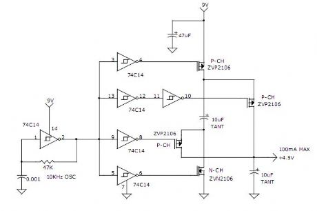
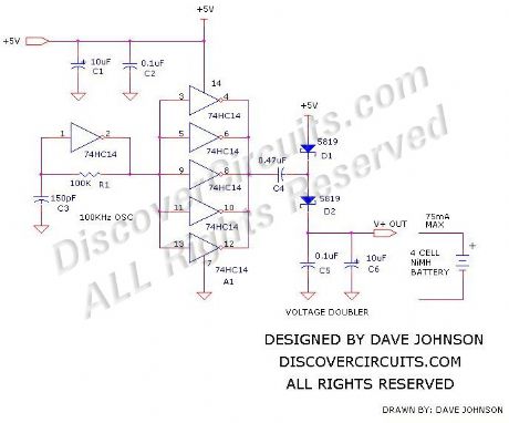
HIGH POWER TOUCH SWITCH EXCITER CIRCUITS
Published:2012/11/8 1:34:00 Author:muriel | Keyword: HIGH POWER, TOUCH SWITCH , EXCITER CIRCUITS
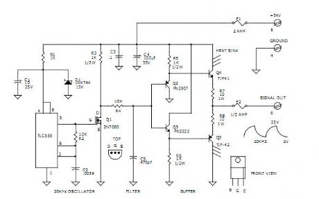
View full Circuit Diagram | Comments | Reading(1158)
Fully Isolated 50/60Hz Sync Generators
Published:2012/11/8 1:33:00 Author:muriel | Keyword: Fully, Isolated, 50/60Hz , Sync Generators
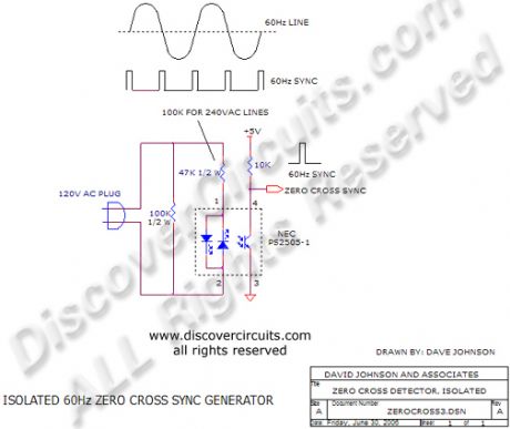
View full Circuit Diagram | Comments | Reading(889)
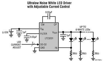
Compact, Inductor less Boost Circuit Regulates White-LED Bias Current
Published:2012/11/8 1:31:00 Author:muriel | Keyword: Compact, Inductor , less Boost Circuit, White-LED Bias Current
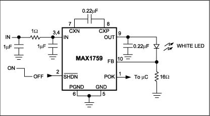
The increasing use of color LCDs in hand-held equipment is creating a need for smaller and cheaper sources of white backlight. Cold-cathode fluorescent lamps (CCFLs) and electro-luminescent (EL) panels have been used in the past, but those circuits are excessively large, expensive, and complex for today's hand-held, consumer-electronics devices. Fortunately, recent advances in LED technology have produced an LED that emits white light. White LEDs have several advantages over conventional types, including small size, low cost, low complexity, and high reliability.The typical forward-bias voltage for white LEDs is about 3.5V ±10%. To obtain white light you simply forward-bias the device, but a boost circuit is required because the white LED's forward voltage can be greater than the battery voltage. The conventional approach to this problem—a boost regulator that biases the LEDs through a ballast resistor—has two drawbacks. First, the wide variation of forward voltage in white LEDs causes a large variation in bias current and the resulting light output. Second, the conventional boost converter has a DC path between input and output (even in shutdown) that allows an inactive LED to drain the battery.The compact circuit (Figure 1) overcomes these problems. The regulated buck/boost charge pump in a small µMAX package (U1) has a 100mA output-current capability. Configured as shown, the circuit directly regulates bias current flowing through the white LED. By biasing multiple white LEDs in parallel, it can provide good light distribution. The U1's design eliminates the troublesome input-output path in shutdown, and its active-low SHDN input (Pin 2) lets the user turn the backlight on and off. The circuit also includes a power-OK output (POK) for signaling a microprocessor when the backlight is available. (View)
View full Circuit Diagram | Comments | Reading(957)
CMOS NAND GATE FORMS GATED 125KHZ OSCILLATOR
Published:2012/11/8 1:29:00 Author:muriel | Keyword: CMOS NAND GATE, 125KHZ , OSCILLATOR
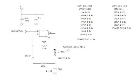
View full Circuit Diagram | Comments | Reading(1338)
Simple Circuit Provides +5V Gate Bias from -48V Input
Published:2012/11/8 1:28:00 Author:muriel | Keyword: Simple Circuit, +5V Gate Bias, -48V Input
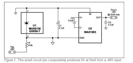
A similar version of this article appeared in the September 19, 2002 issue of EDN magazine.A small and simple circuit (Figure 1) derives +5V from the -48V rail widely used in telecom applications. Useful for gate bias and other purposes, the 5V supply delivers up to 5mA. A shunt reference (U1) defines -5V as ground reference for a charge pump (U2), and the charge pump doubles this 5V difference (between system ground and charge pump ground) to produce +5V with respect to the system ground.The shunt reference maintains 5V across its terminals by regulating its own current (IS), which in turn is determined by the value of R. Current through R (IR) is fairly constant, and varies only with the input voltage. IR, the sum of the charge-pump and shunt-reference currents (IR = ICP + IS), has maximum and minimum values set by the shunt reference. (View)
View full Circuit Diagram | Comments | Reading(819)
Choosing the Right Power-Supply IC for your Application
Published:2012/11/8 1:27:00 Author:muriel | Keyword: Power-Supply IC
Choosing a power-supply IC can be a daunting task for the inexperienced. This application note will help the novice engineer take the first step toward becoming a confident power-supply designer. This article discusses how to choose these ICs at the most fundamental level. First, it explains why power-supply ICs are necessary. It then shows how to choose among the three most common power-supply ICs powered with DC voltages: linear regulators, switching regulators, and charge pumps. Links to supportive application notes and tutorials will address more advanced power-supply topics. (View)
View full Circuit Diagram | Comments | Reading(992)
Charge Pump Doubles Negative Voltage
Published:2012/11/8 1:26:00 Author:muriel | Keyword: Charge Pump , Doubles Negative, Voltage
For low-power dc-dc circuits, the small size and high efficiency of charge pumps makes them ideal for simple doubling and inverting applications. The absence of such ICs designed for negative voltage, however, requires that you adapt an existing positive-voltage device.
(View)
View full Circuit Diagram | Comments | Reading(1921)
Charge-Pump and Step-Up DC-DC Converter Solutions for Powering White LEDs in Series or Parallel Connections
Published:2012/11/8 1:25:00 Author:muriel | Keyword: Charge-Pump , Step-Up, DC-DC Converter Solutions
View full Circuit Diagram | Comments | Reading(1371)
Boost Converter Generates Three Analog Rails
Published:2012/11/8 1:21:00 Author:muriel | Keyword: Boost Converter, Three Analog Rails
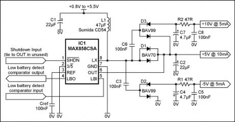
In Figure 1, a standard boost converter consisting of IC1, C1, L1, D1, and C2 generates, in addition to the main output, two auxiliary supply rails (10V and -5V) with the addition of some small and very low-cost extra components. Such rails are useful for the analog circuitry in small handheld instruments, which often require supply voltages in excess of the signal range.The main regulated output of 5V ±2% is sustained by input voltages in the range 0.8V to 5.5V (i.e., from a battery pack of 1 to 3 cells). With an input of 1.8V (two flat cells) and the other rails unloaded, it can produce 25mA with a high efficiency of 80% to 90%.The -5V and 10V outputs are derived from low-cost, discrete charge pumps driven by the converter's switching node (LX) via flying capacitors C3 and C6. The LX node switches between 0V and a level one diode drop above the 5V rail, so the charge pumps' drive voltage is reasonably well regulated. Moreover, the drop across D1 somewhat compensates for diode drops in the two charge-pump outputs.Even more useful is the behavior of IC1 with an increasing load on the auxiliary rails. Its internal control scheme (current-limited, minimum-off-time, pulse-frequency modulation) constantly adapts its switching frequency to the net load current drawn from the rails: frequency increases when the load increases, producing a greater transfer of energy via the flying capacitors. The result is a sort of pseudo-regulation for the charge-pump outputs.These analog supply rails are intended for driving precision op amps, whose input CMR and output range are 2V to 3V within the supply rails. Thus, the rails are good enough if the -5V output is below -3V and the 10V output is above 8V. Accordingly, the components shown were chosen for minimum cost and lowest ripple rather than maximum regulation. Examples are the lossy RC output filters, and the choice of silicon signal diodes instead of Schottky diodes. The 4.7µF capacitors C4 and C7 can be high-ESR, commodity multilayer ceramic types with 16V rating, 1206 case, and Y5V dielectric—such as the 1206YG475ZAT2A from AVX.Output ripple varies with the supply voltage and output load. Operating with an input voltage of 1.8V, the circuit produces ripple amplitudes over the load range of 2mV to 10mVp-p for the 10V rail and 15mV to 30mVp-p for the -5V rail. By increasing C5 and C8 to 2.2µF, you can reduce these ripple levels to 1mV and 5mV respectively. (View)
View full Circuit Diagram | Comments | Reading(846)
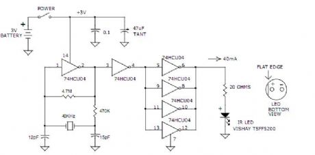
40KHZ LED TEST SIGNAL GENERATOR
Published:2012/11/8 1:19:00 Author:muriel | Keyword: 40KHZ, LED , TEST SIGNAL, GENERATOR
View full Circuit Diagram | Comments | Reading(1092)
100mA Ultralow Noise Charge Pump LED Supply
Published:2012/11/8 1:18:00 Author:muriel | Keyword: 100mA , Ultralow Noise , Charge Pump, LED Supply
View full Circuit Diagram | Comments | Reading(958)
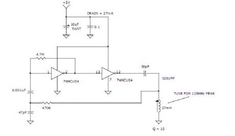
CMOS INVERTERS FORM 125KHZ OSCILLATORS
Published:2012/11/8 1:17:00 Author:muriel | Keyword: CMOS, INVERTERS, 125KHZ OSCILLATORS
View full Circuit Diagram | Comments | Reading(1287)
CHARGE PUMP EFFICIENTLY DIVIDES SUPPLY VOLTAGE
Published:2012/11/8 1:16:00 Author:muriel | Keyword: CHARGE , PUMP EFFICIENTLY , DIVIDES SUPPLY VOLTAGE
View full Circuit Diagram | Comments | Reading(1055)
CAPS PROVIDE VOLTAGE BOOST TO SERIES REGULATORS
Published:2012/11/8 1:15:00 Author:muriel | Keyword: CAPS PROVIDE VOLTAGE , BOOST TO SERIES, REGULATORS
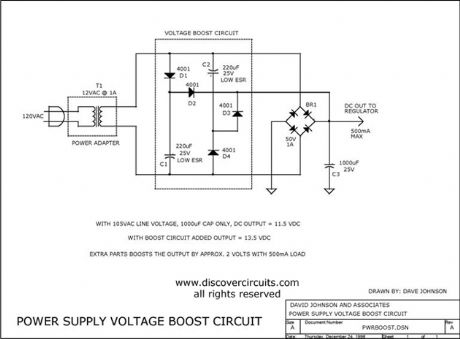
View full Circuit Diagram | Comments | Reading(794)
AUDIO FREQUENCY DIGITAL NOISE GENERATORS
Published:2012/11/8 1:14:00 Author:muriel | Keyword: AUDIO FREQUENCY , DIGITAL NOISE , GENERATORS
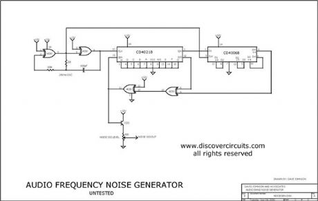
When you need to test an audio circuit with broadband noise, this circuit works great. It uses just three inexpensive C-MOS ICs that generate a series of output pulses whose widths vary randomly. I included a level control pot. (View)
View full Circuit Diagram | Comments | Reading(985)
300-V PEAK TO PEAK SIGNAL GENERATOR
Published:2012/11/8 1:13:00 Author:muriel | Keyword: 300-V, PEAK TO PEAK , SIGNAL GENERATOR
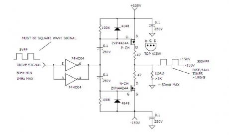
View full Circuit Diagram | Comments | Reading(1049)
200MHz to 400MHz VOLTAGE CONTROLLED OSCILLATOR
Published:2012/11/8 1:12:00 Author:muriel | Keyword: 200MHz to 400MHz , VOLTAGE CONTROLLED OSCILLATOR
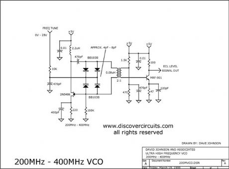
View full Circuit Diagram | Comments | Reading(2138)
12V TOUCH SWITCH EXCITER CIRCUITS
Published:2012/11/8 1:12:00 Author:muriel | Keyword: 12V , TOUCH SWITCH, EXCITER CIRCUITS
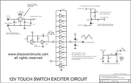
View full Circuit Diagram | Comments | Reading(1042)
+5v Powered Charge Pump Battery Charger
Published:2012/11/8 1:10:00 Author:muriel | Keyword: +5v , Powered Charge , Pump Battery Charger
View full Circuit Diagram | Comments | Reading(925)
High Performance LED Flash Driver
Published:2012/11/8 1:10:00 Author:muriel | Keyword: High Performance, LED Flash, Driver
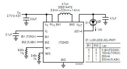
View full Circuit Diagram | Comments | Reading(775)
| Pages:282/2234 At 20281282283284285286287288289290291292293294295296297298299300Under 20 |
Circuit Categories
power supply circuit
Amplifier Circuit
Basic Circuit
LED and Light Circuit
Sensor Circuit
Signal Processing
Electrical Equipment Circuit
Control Circuit
Remote Control Circuit
A/D-D/A Converter Circuit
Audio Circuit
Measuring and Test Circuit
Communication Circuit
Computer-Related Circuit
555 Circuit
Automotive Circuit
Repairing Circuit