
Circuit Diagram
Index 292
Circuit Solar Powered Lithium Ion Battery Charger
Published:2012/10/25 20:58:00 Author:muriel | Keyword: Lithium , Ion , Battery Charger
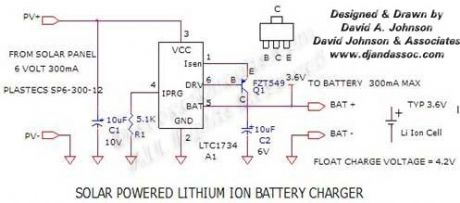
The circuit below feeds a controlled current and voltage to a 3.6v lithium ion battery. The current is limited to 300ma and the voltage is limited to 4.2 volts. The circuit uses a LTC1734 IC from Linear Technology. No diode is needed between the circuit and a 6 volt solar panel. (View)
View full Circuit Diagram | Comments | Reading(1860)
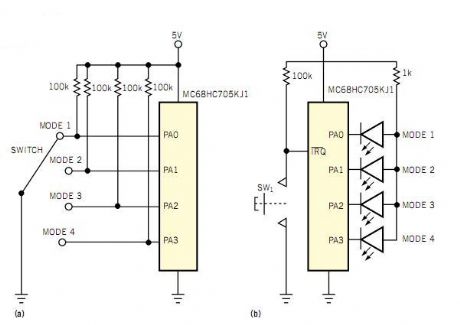
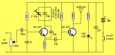
Cheap pushbutton replaces rotary switch
Published:2012/10/25 20:50:00 Author:muriel | Keyword: Cheap pushbutton, replaces , rotary switch
View full Circuit Diagram | Comments | Reading(970)
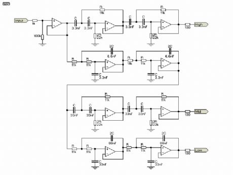
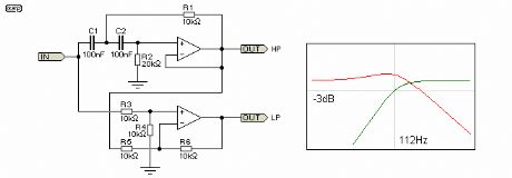
simple bandpass filter
Published:2012/10/25 20:49:00 Author:muriel | Keyword: simple, bandpass filter
View full Circuit Diagram | Comments | Reading(959)
Bandpass Filter
Published:2012/10/25 20:47:00 Author:muriel | Keyword: Bandpass Filter

This circuit is taken from the Progressive Communications Receiver in most of the recent ARRL Handbooks. Values for the 40 meter band are shown.
If you want the ultimate in a bandpass filter for 40 or 20 meters, check out the bandpass filters in An Integrated Contest-Grade CW Station , Solid State Design for the Radio Amateur, by Wes Hayward and Doug DeMaw, Page 225. (View)
View full Circuit Diagram | Comments | Reading(3099)
Buffer Stage. One Per Output Needed
Published:2012/10/25 3:13:00 Author:muriel | Keyword: Buffer, One Per Output

These buffers should use high quality opamps, and they are included on the PCB, including the trimpot (see the photo at the beginning of this article).
Several people (including me) have found that the crossover unit has a short 'chirp' or 'snap' (depending on the opamp characteristics) as power is removed, and this may be accompanied by some DC swing. If you use the new version of the P05B preamp power supply, the auxiliary output can be used to activate a 6-pole relay (or as many smaller relays as needed) to short all outputs to earth when there is no power. The normally closed contacts simply short the outputs to ground, and when power is applied the short is removed. P05 (Rev-B) boards have a power-on delay and a loss of AC detector that will mute the crossover for a few seconds at power-on, and almost immediately when power is turned off. (View)
View full Circuit Diagram | Comments | Reading(887)
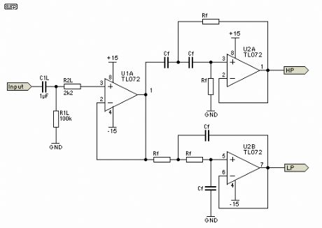
3-Way Linkwitz Riley Crossover
Published:2012/10/25 3:12:00 Author:muriel | Keyword: 3-Way , Linkwitz Riley Crossover
the way to connect a 3-Way crossover. This unit produces excellent results, with good phase coherency and a flat response across the entire frequency band.
I know the circuits look complicated, but each is basically repetition of a common circuit block - the filter section. Since the opamps are all used as unity gain buffers, the use of premium devices is not really essential, so the TL072 type would be quite serviceable in this role. Needless to say, if you want to use better devices (even discrete opamps) you can easily do so. Make sure that any device used is stable for unity gain - this is not always the case with some devices, especially when external compensation is used. In this case, use the manufacturer's recommended value of stability cap for unity gain operation. (View)
View full Circuit Diagram | Comments | Reading(9099)
2-Way Linkwitz Riley Crossover
Published:2012/10/25 3:12:00 Author:muriel | Keyword: 2-Way, Linkwitz Riley Crossover

the general concept for a full stereo version, with two identical filter sections (but without balanced inputs). With the component values shown, these have a crossover frequency of 310Hz (refer to the article on Bi-Amping to see the reason for my choice of frequency). This unit will provide a completely flat frequency response across the crossover frequency, with the signal from both filters remaining in phase at all times.
Note that the PCB version is almost identical, but offers the choice of a balanced or unbalanced input stage. It's not switchable, but the mode is selected before construction, and links or resistors are installed as needed.
(View)
View full Circuit Diagram | Comments | Reading(3661)
Output Buffers circuit
Published:2012/10/25 3:10:00 Author:muriel | Keyword: Output Buffers circuit
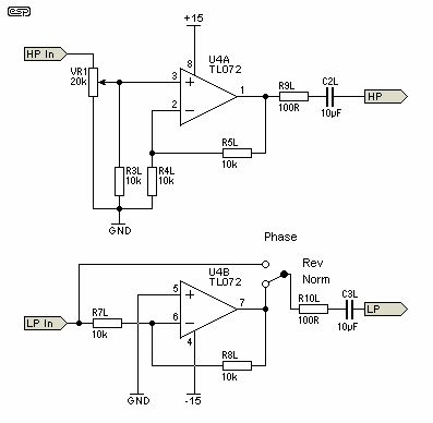
the output buffers (again, left channel only) connected in the manner I used for the prototype. The high pass section provides a gain of 6dB, and has a pot to adjust the level to allow for different loudspeaker sensitivities. The gain can be adjusted from +6dB to -8dB (approximately), which will be more than enough for any installation. The low pass buffer has a gain of -1, which is to say that gain is unity, but inverted. A phase switch can be incorporated as shown to allow for sub-woofer phase correction - this is not needed for a biamp setup. (View)
View full Circuit Diagram | Comments | Reading(810)
- 12dB / Octave Crossover Network
Published:2012/10/25 3:09:00 Author:muriel | Keyword: - 12dB , Octave, Crossover Network
The circuit diagram of the filter section is shown in Figure 1. It is a completely conventional filter, and the component designations are the same as for the 24dB unit described in Project 09. It is designed primarily for 2-way electronically crossed over systems, such as adding a subwoofer or biamping an existing loudspeaker system.
Figure 2 shows the output buffers - again using the same component designators, but with some changes. The low pass section is inverted, since 12dB crossovers always invert the phase of one signal. If desired, the high pass section may be inverted instead - see Figure 3 for the alternative version. (View)
View full Circuit Diagram | Comments | Reading(2397)
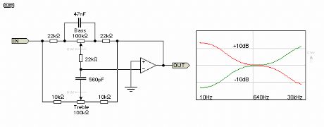
Guitar Control
Published:2012/10/25 3:08:00 Author:muriel | Keyword: Guitar Control
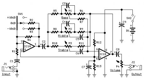
Stand-alone, 9V battery powered unit
Three-level input selector, three-band tone control (View)
View full Circuit Diagram | Comments | Reading(1478)
Expandable Graphic Equaliser
Published:2012/10/25 3:00:00 Author:muriel | Keyword: Expandable Graphic Equaliser
View full Circuit Diagram | Comments | Reading(694)
Power Supply Unit
Published:2012/10/25 2:43:00 Author:muriel | Keyword: Power Supply Unit
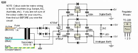
I suggest that a the power supply shown here be used instead of a modified version of the unit described in Project 05, as this will operate all the devices shown in Figure 3. The simple trick used in the previous project was quite suitable for audio only circuits, but with the addition of the digital circuitry we need more power and better regulation than can be obtained from the full-wave voltage doubler circuit used. (View)
View full Circuit Diagram | Comments | Reading(1250)
Complete Surround System
Published:2012/10/25 2:42:00 Author:muriel | Keyword: Complete, Surround System
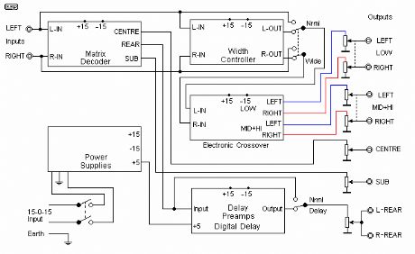
A complete surround system would consist of a power supply, the decoder matrix, optionally the stereo width controller, and the delay unit. Figure 3 shows my suggested method of interconnecting the units, which can all be housed in a single case. For the more adventurous, you can add a pair of Linkwitz-Riley crossovers for bi-amping (shown in the dotted box) for the front left and right speakers.
This keeps everything together, and only the switches needs to be accessible in normal use. All level controls should be set to the desired volume, and not fiddled with once you have it the way you want. If these are accessible, everyone will want to fiddle, and you will then have to try to set it back to where you want - until someone else comes and fiddles again. (View)
View full Circuit Diagram | Comments | Reading(2535)
Input Buffer And Output Driver
Published:2012/10/25 2:42:00 Author:muriel | Keyword: Input Buffer, Output Driver
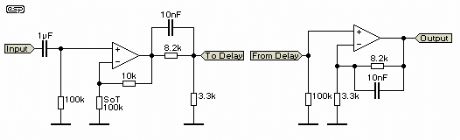
The input driver circuit is designed to reduce the signal level applied to the delay chip, to prevent any risk of overload. Since the maximum specified level is 1 Volt RMS, it is important to ensure that the signal is below this at all times. The output from a CD player is generally about 2.5V (maximum), so the input circuit reduces the level by a factor of about 3.5 (10.8dB). Since this must be amplified again after the delay, there is a pre-emphasis circuit included to increase the level of high frequencies. The frequency response is restored to normal with treble cut after the delay, reducing noise as well. This technique is used with FM radio broadcasts, vinyl disks and in many other areas and is effective in minimising noise levels. (View)
View full Circuit Diagram | Comments | Reading(933)
The Delay Circuit
Published:2012/10/25 2:41:00 Author:muriel | Keyword: Delay Circuit
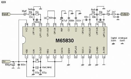
The delay circuit is shown in Figure 1, and uses the Mitsubishi M65830 Digital Delay chip. This has been around for a while now, and is simple and effective (provided that a fixed delay is acceptable). The serial data required to obtain different delay settings is not easily obtained, and would add considerably to the complexity of the circuit. As such, it would no longer be a simple matter to construct using Veroboard or similar, and would require a printed circuit board.
The circuit is (almost) a direct adaptation from the Mitsubishi data sheet, and as shown will give good performance over a wide frequency range. The filters are tuned to around 9.5 kHz, and although this could be reduced there does not seem to be any good reason to do so. This seems to be the optimum response for rear channel speakers, so should be left alone. The filter circuits use internal opamps, and only require the external components shown below. (View)
View full Circuit Diagram | Comments | Reading(1947)
The Beetle MkIII Circuit
Published:2012/10/25 2:40:00 Author:muriel | Keyword: Beetle MkIII Circuit
View full Circuit Diagram | Comments | Reading(1165)
Crossover Networks
Published:2012/10/25 2:39:00 Author:muriel | Keyword: Crossover Networks
When combined, high pass and low pass filters are commonly used to create electronic crossover networks. There are many different ways to do this, but the most common is still the second order Butterworth filter. Although these are essentially at least as good as the passive speaker level counterpart (but not all that much better), the results are often vastly superior. The reasons for this are discussed at great length in my article Bi-Amplification - Not Quite Magic (but Close) and I shall not repeat them here.
In a nutshell, using an electronic crossover eliminates many of the problems that beset loudspeaker designers when they have to design and build the crossover network. The passive crossover is influenced by any aberration in the driver's impedance, especially at or near the crossover frequency. Since the electronic crossover supplies the signal to a separate amplifier for each frequency band, there is no interaction and each amp only needs to be concerned with a much smaller bandwidth.
All crossover networks are a combination of high pass and low pass filters, although this is not always achieved in the same way. Some crossovers use an opamp as a subtracting amplifier, so rather than using a separate filter, the bass (for example) is subtracted from the main signal to provide the midrange and high frequency. Alternatively, the mid+high output from the filter is subtracted from the main signal to separate the bass, and this configuration is shown below. These crossovers are phase coherent (both outputs are always in phase at any frequency), but are asymmetrical. A typical design is shown in Figure 19, and the response clearly shows that the high pass rolloff is 12dB/octave, but the low pass is only 6dB/octave. (View)
View full Circuit Diagram | Comments | Reading(1563)
Designing Our First Filter
Published:2012/10/25 2:35:00 Author:muriel | Keyword: Filter

The first active filter must be the first order low pass. By simply reversing the filter components, this becomes a first order high pass. In each case, the filter only consists of the resistance and capacitance, with the opamp simply isolating the filter from the following stages. Q is not variable in a first order filter, and the only options are high pass and low pass. A bandpass filter can only be created by cascading a high and low pass filter. Although the least useful of all filters, they are easy to understand, so make a good starting point. (View)
View full Circuit Diagram | Comments | Reading(783)
Baxandall Tone Controls
Published:2012/10/25 2:35:00 Author:muriel | Keyword: Baxandall Tone Controls
This is the most common of all modern tone control circuits, and was named after PJ Baxandall who came up with the idea many years ago. The original design article was entitled Negative Feedback Tone Control - Independent Variation of Bass and Treble Without Switches , and was published in Wireless World (now Electronics World) in 1952. This type of control is fully symmetrical, and there is no interaction between the controls, unlike the older passive controls. When centred, there is neither loss nor gain, and the opamp acts as a buffer. Frequency response is absolutely flat, provided the pots centre precisely. (View)
View full Circuit Diagram | Comments | Reading(3687)
Automatic Loudness Control
Published:2012/10/25 2:34:00 Author:muriel | Keyword: Automatic Loudness Control
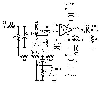
View full Circuit Diagram | Comments | Reading(1109)
| Pages:292/2234 At 20281282283284285286287288289290291292293294295296297298299300Under 20 |
Circuit Categories
power supply circuit
Amplifier Circuit
Basic Circuit
LED and Light Circuit
Sensor Circuit
Signal Processing
Electrical Equipment Circuit
Control Circuit
Remote Control Circuit
A/D-D/A Converter Circuit
Audio Circuit
Measuring and Test Circuit
Communication Circuit
Computer-Related Circuit
555 Circuit
Automotive Circuit
Repairing Circuit