
Circuit Diagram
Index 281
Tripler Converts 5V to 15V
Published:2012/11/9 0:11:00 Author:muriel | Keyword: Tripler , 5V to 15V
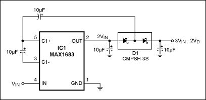
This application note shows how to configure the MAX1683 to triple the input voltage for low-current applications while minimizing voltage drop.
A similar version of this article appeared in the August 17, 2000 issue of ECN magazine.
By configuring a charge-pump voltage doubler as a tripler, you can readily derive 15V from 5V. A 15V rail is useful for powering op amps, LCD-bias circuits, and other low-current applications.
The connections in Figure 1 configure the MAX1683 voltage doubler as a tripler. The no-load output voltage of the circuit is approximately 3VIN - 2VD, where VD is the voltage drop across one diode. Use Schottky diodes as shown to minimize VD and its effect on output voltage. (View)
View full Circuit Diagram | Comments | Reading(1179)
Triple Capacitive Voltage Inverter with the MAX871
Published:2012/11/9 0:10:00 Author:muriel | Keyword: Triple Capacitive Voltage , Inverter, MAX871
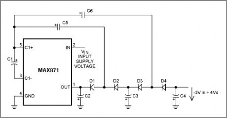
This design idea is based on a customer request for a cheap, and not very accurate, negative voltage supply of about -12V to -15V with a low output current of < 5mA and an input voltage of 5V. This application might be used for negative op-amp supply. Figure 1 shows the typical operation circuit with the flying capacitor C1 and C2. The output voltage on pin 1 is -VIN. Four additional capacitors (C3 to C6) and four additional diodes (D1 to D4) triple the negative output voltage at the OUT pin from -VIN to -3VIN. C5 and C6 decreases the voltage with every step by -VIN. Without any diode voltage drop C3 got -2VIN and C4 charges ideally to -3VIN. It is possible to add more of these cascades but with every step the voltage drop of the diodes will reduce the effort. (View)
View full Circuit Diagram | Comments | Reading(1064)
DC-DC Boost Converter plus LDO
Published:2012/11/9 0:09:00 Author:muriel | Keyword: DC-DC , Boost Converter , LDO
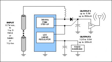
Combining a DC-DC boost converter with an LDO has two advantages: It implements a low-noise boost function (at a slight penalty in efficiency versus the noisy booster without an LDO), and it performs the buck/boost function with surprisingly high efficiency. A typical buck/boost application converts the output of one Li-ion cell to 3.3V. Efficiency is very high, because the battery spends most of its life near 3.6V, allowing the booster to idle and providing the LDO with a near-ideal input voltage. This system also delivers higher efficiency with smaller external components than the traditional SEPIC converter. Because of the favorable characteristics of this arrangement, several single-chip implementations are available for the DC-DC boost converter plus LDO architecture. (View)
View full Circuit Diagram | Comments | Reading(1749)
Regulated Charge Pump Delivers 50mA
Published:2012/11/9 0:07:00 Author:muriel | Keyword: Charge Pump, 50mA
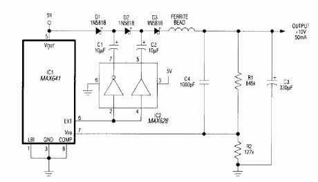
The DC-DC converter circuit of Figure 1 substitutes a voltage tripler in place of the external inductor and diode normally associated with switching regulator IC1. Inverting and noninverting drivers in the MOSFET-driver chip (IC2) activate a diode/capacitor tripling network (D1-D3, C1-C3). In comparison with charge pumps based on single-polarity drivers, the buffer/inverter combination of IC2 enables this circuit to deliver more current with fewer parts.A 50kHz oscillator within IC1 produces the EXT signal (pin 6), which IC2 converts to drive signals (180° out of phase) for the tripler. The resulting charge-discharge action in the capacitors recharges C3 toward 10V every 20µs. The ferrite bead limits output ripple to about 20mVP-P for a 50mA load. (View)
View full Circuit Diagram | Comments | Reading(1301)
One 9V battery gives +18, +25, +33V
Published:2012/11/9 0:06:00 Author:muriel | Keyword: One , 9V, battery , +18, +25, +33V
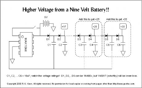
For you high-voltage minibooster fans out there, here's the one-chip, one battery way to do it.
The MAX1044 is a charge pump converter - it uses a capacitor as a bucket to pump charge from one place to another. Normally, there is a capacitor connected from pin 2 of the 1044 to pin 4. This capacitor is charged between +9V and ground, and then switched in parallel with a capacitor from pin 5 to ground in a way that makes a negative voltage on the second cap.
In this UPverting use, the 1044 still switches pin 2 between +9V and ground just as it would for a voltage inverter. However, we ignore the pin 4 and 5 connections that would make an inverter from it. Instead, we connect two capacitors and diodes as shown (D1, 2, and C1, 2). The voltage on pin 2 of the 1044 is switched from +9V to ground. When it switches to ground, C1 fills with voltage through D1. When it then switches to +9, it pulls the negative terminal of C1 up to +9V. D1 now blocks any flow of current back into the battery, so the charge in C1 flows through D2 into C2. So at C2, we now get almost 18V!
There's more. If we add another two diodes and capacitors (D3, D4 and C3, C4), we can add another 9V to it, as C3 charges to +18 through D3 when pin 2 is at ground, and is pulled up to +25 (+27 minus the voltage drops of the diodes) when pin 2 goes high. We can do it again with D5, D6 and C5, C6 to get +33V. The limit on all this is the losses in the diode voltages. Each time we add a section, we add two more diode drops that we can't take advantage of to charge capacitors. But +33 is not bad for a single 9V battery!
If you build this, you MUST take notice of the voltages on the capacitors. The caps can all be the same value, but C1, C2 need to be 25V units, C3, 4, 5, and 6 can be 35V units, and C5 and C6 might need to be 50V unit just for some safety margin. 1N400x diodes work and are cheap, but the losses are higher than they really need to be. For higher performance and lower losses, it's better to use something like the 1N5817 schottky diodes for low losses. But both will work.
This charge pumping is a very efficient way to convert voltages. The only power lost is that power dissipated in the resistances of the switches inside the 1044 and the series resistance of the capacitors and diodes, as well as the power to run the internal oscillator that flips the switches when needed.
All by itself, the 1044 runs at about 7-10kHz, so there will be ripple of that amount on the C2 output and on the +9V output from the battery as well. Audio equipment that uses this voltage could have a whine audible if you're not careful. However, the 1044 has a frequency boost feature. If you connect pin 1 to the power supply (shown by the little open switch) then the oscillator frequency goes up by about 6:1. The oscillator then works well above the audio region. Any whine is then going to be inaudible. (View)
View full Circuit Diagram | Comments | Reading(1221)
SIMPLE WHITE LED NIGHT LIGHTS
Published:2012/11/9 0:04:00 Author:muriel | Keyword: SIMPLE WHITE LED NIGHT LIGHTS
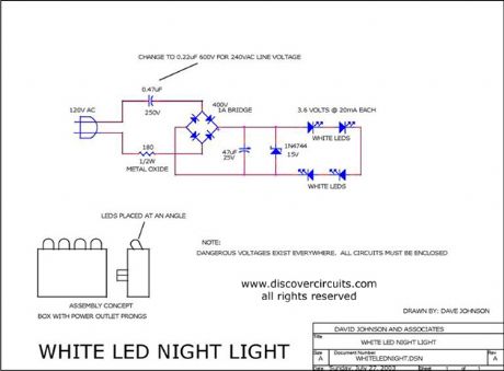
This simple circuit is designed to plug into a standard AC electrical outlet. It uses four super bright white light emitting diodes (LED) in conjunction with a capacitor coupled full wave rectifier circuit. The LEDs are mounted in a box and are angled slightly to bounce the light off of a nearby wall. The light should last about 10 years. The circuit draws less than one half of one watt of power and can therefore run continuously. In spite of the low power, the LEDs provide sufficient illumination for most night light applications. Circuit component values for both 120vac and 240vac are shown. (View)
View full Circuit Diagram | Comments | Reading(4512)
VERY LOW POWER GATED CRYSTAL OSCILLATORS
Published:2012/11/9 0:03:00 Author:muriel | Keyword: VERY LOW POWER , GATED CRYSTAL OSCILLATORS

The circuit gates the output of a continuously operating 32KHz crystal oscillator to the input of a C-MOS buffer when clock pulses are needed. The technique gets around the problem of a slow starting crystal oscillator by keeping the oscillator going and switching on a transistor power stage only as needed. The method keeps the standby power consumption to a very low 1uA when used with a 3v supply. (View)
View full Circuit Diagram | Comments | Reading(1251)
VERY LOW POWER ASTABLE MULTIVIBRATOR
Published:2012/11/9 0:01:00 Author:muriel | Keyword: VERY LOW POWER , ASTABLE MULTIVIBRATOR
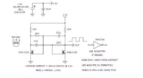
This classic circuit draws only 200 nanoamps from a 1.5v supply.
(View)
View full Circuit Diagram | Comments | Reading(1894)
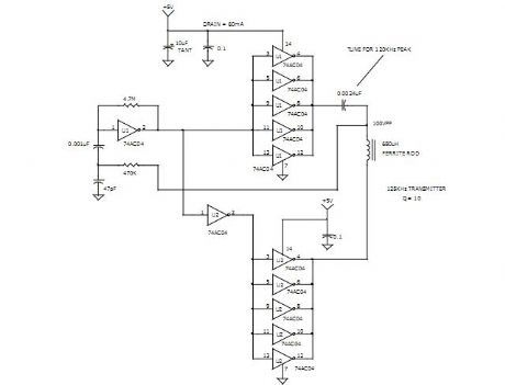
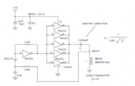
ULTRA PURE 125KHz SINE WAVE SIGNAL SOURCE
Published:2012/11/9 Author:muriel | Keyword: ULTRA PURE , 125KHz , SINE WAVE SIGNAL SOURCE
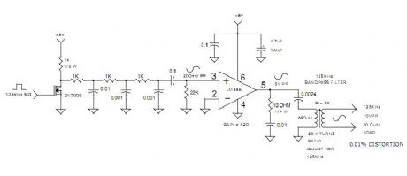
For some RFID systems operating at 125KHz, a very low distortion signal source reference is needed. The circuit shown on this page produces a 10-volt peak-to-peak signal into a 50-ohm load, with a distortion of only 0.01%.
(View)
View full Circuit Diagram | Comments | Reading(2123)
SQUARE WAVE DRIVER HAS FLEXIBLE OUTPUTS
Published:2012/11/8 23:59:00 Author:muriel | Keyword: SQUARE WAVE DRIVER, FLEXIBLE OUTPUTS
This circuit can produce an output signal ranging from DC to 100KHz. It can source a voltage ranging from 1v to 30v. It can sink a voltage ranging from zero volts to �30v. It can drive up to 200ma of current and can even be switched to a floating tristate output.
(View)
View full Circuit Diagram | Comments | Reading(1021)
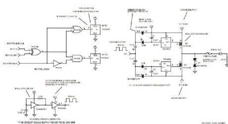
Simple Methods Reduce Input Ripple for All Charge Pumps
Published:2012/11/8 23:57:00 Author:muriel | Keyword: Reduce Input Ripple, All Charge Pumps
Charge pumps are a form of DC-DC converter that rely on capacitors instead of inductors for energy storage and transfer. The absence of inductors makes them attractive in situations requiring a low-power auxiliary supply (output currents up to about 150mA). They use less circuit-board area, offer minimal component height, and are easy to use.Charge pumps can have regulated or unregulated outputs. An unregulated charge pump either doubles or inverts the voltage that powers it and the output voltage is a function of the supply voltage. A regulated charge pump either boosts or inverts the supply voltage. Its output voltage is independent of the supply.Techniques that reduce capacitor size and optimize output current—fast switching speed and low-on-resistance switches—also produce noise and transient ripple at the input supply pin. Noise can propagate back along the input supply pins, creating problems for crystal-controlled oscillators, VCOs, and other sensitive circuits with poor power-supply rejection. This article focuses on methods for reducing the noise. (View)
View full Circuit Diagram | Comments | Reading(791)
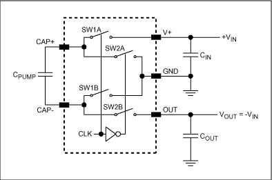
Miniature, Precision Negative Reference Requires No Precision Resistors
Published:2012/11/8 23:55:00 Author:muriel | Keyword: Miniature, Precision , Negative, Reference, No Precision Resistors
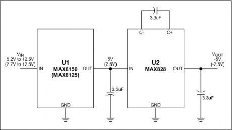
Switched-capacitor charge-pumps, which occupy less space than do their inductor-based counterparts, are popular for providing inverted voltages in small hand-held equipment. Combining a switched-capacitor charge-pump with a precision reference, for example, yields an inverted reference from a positive power supply (Figure 1). Unlike the more typical combination of a positive 3-terminal reference and an op-amp inverter, this one delivers accurate inversions without the need for precision resistors and a negative supply. The charge-pump inverter (U2) delivers -5V by inverting the output of a 5V precision reference (U1). U1 accepts inputs between 5.2V and 12.5V. Replacing it with a 2.5V reference that accepts 2.7V to 12.5V, as in the MAX6125, produces a -2.5V output. This circuit is very compact. It needs only three surface-mount capacitors, and the ICs occupy tiny SOT23 packages. (View)
View full Circuit Diagram | Comments | Reading(747)
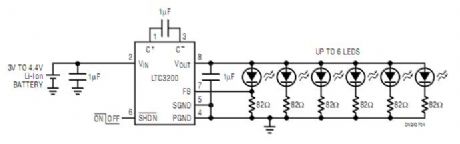
Low Noise White LED Driver with LED Current Control
Published:2012/11/8 23:53:00 Author:muriel | Keyword: Low Noise, White LED Driver , LED Current Control
View full Circuit Diagram | Comments | Reading(834)
Single-phase current drying and heating motor winding circuit
Published:2012/11/8 21:17:00 Author:Ecco | Keyword: Single-phase , current drying, heating , motor winding
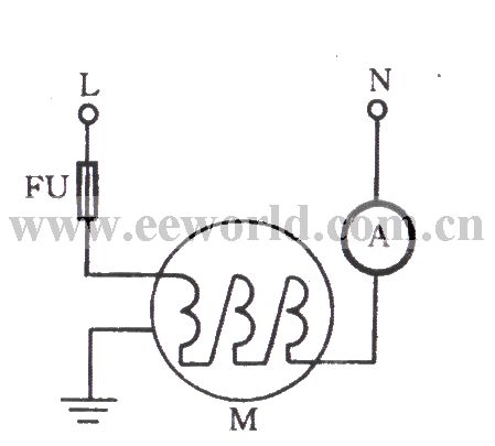
If the motor is dormant for long time or soaked in the ridge edge of a farm in rainy season. After being tested by 500V megger, if the motor insulation resistance is less than 0.5 megohm, the motor has been exposed to be moisture, then the drying treatment must be carried out. The single-phase current heating method for drying treatment of the motor windings is shown as the figure.
(View)
View full Circuit Diagram | Comments | Reading(1302)
Proximity switch circuit
Published:2012/11/8 21:13:00 Author:Ecco | Keyword: Proximity switch
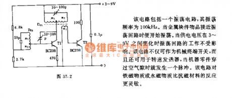
The circuit comprises an oscillator circuit, and its oscillation frequency is 100kHz. It starts oscillation when the metal block closes to the oscillator circuit. When the oscillation loop is not affected when the supply voltage varies between 3 ~ 9V. The circuit can not only be used as a mechanical terminal switch, but can also be used as speed transmitter, when machine parts pass through the air gap, it will generate a pulse.
(View)
View full Circuit Diagram | Comments | Reading(970)
Flashing light indication light switch circuit
Published:2012/11/8 20:55:00 Author:Ecco | Keyword: Flashing light , indication , light switch
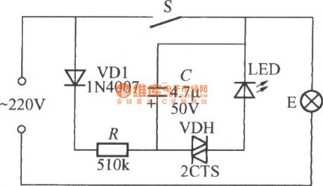
When S is closed, the light E is lit normally, flashing light indication circuit does not work because of losing power. When S is open, 220V AC is rectified by bulb E and diode VD1, and buck limited by R to charge for the capacitor C. The circuit uses the charging and discharging principle of capacitor C and two - way trigger diode VDH negative resistance to form a relaxation oscillator, so light-emitting tube LED flashes at night, and it is very eye-catching to make it easy to find the switch position.
(View)
View full Circuit Diagram | Comments | Reading(1406)
One-key touching light switch circuit (5 )
Published:2012/11/8 20:43:00 Author:Ecco | Keyword: One-key, touching light , switch
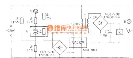
As shown in figure, it uses weak current luminous neon tube and a novel memory SELF-LOCKI relay to form one - key touching light switch, and the on-off of bulb E is not only can be controlled through the touching manner, and The switch 's own consumption is microampere magnitude both in the on or off state. In addition, it can control start or stop of various household appliances. In the Figure, RL is MG45 photoresistor; K should adopt ZS-01F memory self-locking relay with 12V working voltage.
(View)
View full Circuit Diagram | Comments | Reading(1388)
SPI bus high-precision pressure test system circuit diagram
Published:2012/11/8 20:38:00 Author:Ecco | Keyword: SPI bus, high-precision , pressure test system
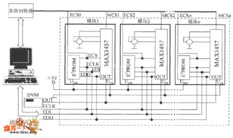
It uses a MAX1457 and a 27C64 to match with piezoresistive pressure sensor and constitute a pressure measurement module. N pieces of pressure measurement module with the computer and digital voltmeter form a PI bus high-precision pressure test system circuit. It consists of six transmission lines including two power supply lines (UDD, USS), an analog voltage output line ( out , pick digital voltmeter ) and three SPI interface lines (ECLK, EDI and EDO ).
(View)
View full Circuit Diagram | Comments | Reading(1448)
MEDIUM POWER 125KHZ OSCILLATOR-2
Published:2012/11/8 1:36:00 Author:muriel | Keyword: MEDIUM POWER , 125KHZ, OSCILLATOR-2
View full Circuit Diagram | Comments | Reading(1331)
MEDIUM POWER 125KHZ OSCILLATORS
Published:2012/11/8 1:35:00 Author:muriel | Keyword: MEDIUM POWER, 125KHZ OSCILLATORS
View full Circuit Diagram | Comments | Reading(1120)
| Pages:281/2234 At 20281282283284285286287288289290291292293294295296297298299300Under 20 |
Circuit Categories
power supply circuit
Amplifier Circuit
Basic Circuit
LED and Light Circuit
Sensor Circuit
Signal Processing
Electrical Equipment Circuit
Control Circuit
Remote Control Circuit
A/D-D/A Converter Circuit
Audio Circuit
Measuring and Test Circuit
Communication Circuit
Computer-Related Circuit
555 Circuit
Automotive Circuit
Repairing Circuit