
Circuit Diagram
Index 302
Linear voltage-controlled oscillator circuit diagram
Published:2012/10/17 22:05:00 Author:Ecco | Keyword: Linear, voltage-controlled oscillator
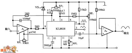
It uses ICL8038 to form a linear voltage controlled oscillator with output frequency and input voltage being proportional. In the circuit, A1 is used to improve C1 charging and discharging constant current circuit characteristics, so that the output frequency and relative input voltage have a linear relationship, A2 is the sine wave output buffer. RP1 is used to adjust the offset voltage, RP2 is used to adjust the high-frequency symmetry, RP3 is used to adjust the low-frequency symmetry, RP3 and RP4 are used to adjust the sine-wave distortion degree.
(View)
View full Circuit Diagram | Comments | Reading(2410)
Voltage - controlled oscillator circuit diagram with operational amplifier
Published:2012/10/17 23:03:00 Author:Ecco | Keyword: Voltage - controlled oscillator , operational amplifier
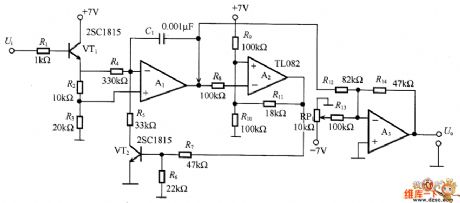
The circuit uses integrator A1 and delay comparator A2 to form a triangular wave oscillator, but the circuit is not directly integrating the output of A2, but it's controlled for integrating, therefore, the obtained oscillation frequency and control voltage are proportional, i.e. the so-called voltage-controlled oscillator. In the circuit, when VT2 gets conduction, the discharging slope rate of C1 is contrary to charging to generate a triangular wave. Saturation voltage of the op amp A2 affects Delay comparator threshold. Thus, the circuit is not suitable for high accuracy circuit. A3 is level-shifting circuit.
(View)
View full Circuit Diagram | Comments | Reading(2945)
Digital Electronic Lock
Published:2012/10/17 22:24:00 Author:muriel | Keyword: Digital, Electronic Lock
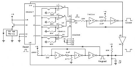
The digital lock shown below uses 4 common logic ICs to allow controlling a relay by entering a 4 digit number on a keypad. The first 4 outputs from the CD4017 decade counter (pins 3,2,4,7) are gated together with 4 digits from a keypad so that as the keys are depressed in the correct order, the counter will advance. As each correct key is pressed, a low level appears at the output of the dual NAND gate producing a high level at the output of the 8 input NAND at pin 13. The momentary high level from pin 13 activates a one shot circuit which applies an approximate 80 millisecond positive going pulse to the clock line (pin 14) of the decade counter which advances it one count on the rising edge. A second monostable, one shot circuit is used to generate an approximate 40 millisecond positive going pulse which is applied to the common point of the keypad so that the appropriate NAND gate will see two logic high levels when the correct key is pressed (one from the counter and the other from the key). The inverted clock pulse (negative going) at pin 12 of the 74C14 and the positive going keypad pulse at pin 6 are gated together using two diodes as an AND gate (shown in lower right corner). The output at the junction of the diodes will be positive in the event a wrong key is pressed and will reset the counter. When a correct key is pressed, outputs will be present from both monostable circuits (clock and keypad) causing the reset line to remain low and allowing the counter to advance. However, since the keypad pulse begins slightly before the clock, a 0.1uF capacitor is connected to the reset line to delay the reset until the inverted clock arrives. The values are not critical and various other timing schemes could be used but the clock signal should be slightly longer than the keypad pulse so that the clock signal can mask out the keypad and avoid resetting the counter in the event the clock pulse ends before the keypad pulse. The fifth output of the counter is on pin 10, so that after four correct key entries have been made, pin 10 will move to a high level and can be used to activate a relay, illuminate an LED, ect. At this point, the lock can be reset simply by pressing any key. The circuit can be extended with additional gates (one more CD4011) to accept up to a 8 digit code. The 4017 counting order is 3 2 4 7 10 1 5 6 9 11 so that the first 8 outputs are connected to the NAND gates and pin 9 would be used to drive the relay or light. The 4 additional NAND gate outputs would connect to the 4 remaining inputs of the CD4068 (pins 9,10,11,12). The circuit will operate from 3 to 12 volts on 4000 series CMOS but only 6 volts or less if 74HC parts are used. The circuit draws very little current (about 165 microamps) so it could be powered for several months on 4 AA batteries assuming only intermittent use of the relay.
(View)
View full Circuit Diagram | Comments | Reading(1012)
LM324 op-amp
Published:2012/10/17 22:22:00 Author:muriel | Keyword: LM324, op-amp
View full Circuit Diagram | Comments | Reading(5031)
555 overvoltage indication circuit
Published:2012/10/16 21:54:00 Author:Ecco | Keyword: 555, overvoltage indication
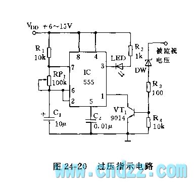
As shown in Figure 24-10, 555, R1, RP1 and C1 form astable multivibrator, but its ground pin is connected to c pole of detection transistor. When the monitored voltage exceeds set value, DW is breakdown, VT1 is saturated and turned, then 555 starts oscillation, LED light flashes. VT1 can also reduce the static power dissipation of 555. 555 oscillation frequency can be adjusted between 1 ~ 20Hz, and RP1 can be used to select the flashing number of LED.
(View)
View full Circuit Diagram | Comments | Reading(1896)
Knife switch start circuit
Published:2012/10/16 22:08:00 Author:Ecco | Keyword: Knife switch start
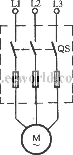
The knife switch inlcudes plastic cover porcelain bottom knife switch, Hulled knife switch and flagstone knife switch. It can directly start small motor with power being less than 7.5kW, the circuit is shown in the figure. The switch is matched with fuse pipe or wiring connected to fuse pile, so it is very convenient to replace fuse. Operation methods: you can close the knife switch, the motor M rotates; if you pull the knife switch motor, M will stop. The circuit can be widely used in pumps, rice mill, grinding machines and other small machinery.
(View)
View full Circuit Diagram | Comments | Reading(1341)
Jog combined with long-running start-up circuit
Published:2012/10/16 22:20:00 Author:Ecco | Keyword: Jog , long-running start-up
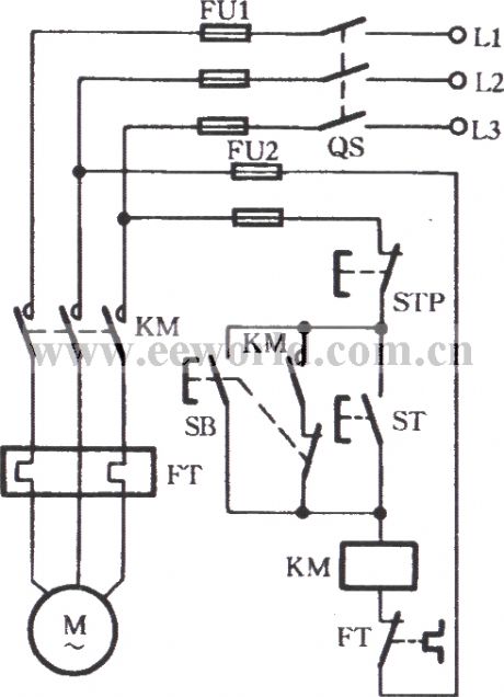
In reality, sometimes it needs to manually jog to operate the motor for long operation. The circuit shown in Figure is designed to address this issue. When the start button ST is pressed, motor M is normal startup, and the circuit utilizes its normally open auxiliary contact to lock it by itself, then the motor M can make long-term operation. Pressing STP can stop motor M. If you press the button SB, motor M starts. Because pressing SB normally open contact also disconnects normally closed contacts, and SB is loosen, KM loses electric, then motor M stops, this mode is called jog .
(View)
View full Circuit Diagram | Comments | Reading(1504)
Battery cold junction thermocouple protection circuit
Published:2012/10/16 22:31:00 Author:Ecco | Keyword: Battery, cold junction , thermocouple protection
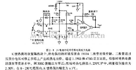
K thermocouple end is placed is insulation block, the thermocouple junction ambient temperature is continuously controlled by IN914 diode. The diode correct hermoelectromotive force generated on junction by feedback voltage. Then it is sent to the op amp by 1.5MΩ and 475Ω resistors. The thermocouple junction is pulled in zero ice water during calibration. Tuning 500Ω can make output be zero pressure; then the thermocouple is inserted in 250 ℃ furnace, tune range for output is 2.50V. In 9 ~ 250 ℃ range, the accuracy of K thermal couple is ± 3 ℃.
(View)
View full Circuit Diagram | Comments | Reading(1941)
555 program controller circuit
Published:2012/10/16 21:35:00 Author:Ecco | Keyword: 555, program controller
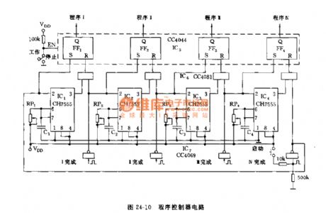
As shown in 24-10, it uses four 555 circuits which respectively form different timing monostable circuit, and they are concatenated cycle triggers. IC7 is timed and set by trigger monostable circuit composed of C4069's hex inverter. IC6 is four 2 -input AND gate; IC5 (CC4044) is four RS latch. When the start button is pressed, IC1 sets.
(View)
View full Circuit Diagram | Comments | Reading(1549)
Bidirectional line driver circuit composed of double broadband transconductance operational amplifier OPA2662
Published:2012/10/15 21:42:00 Author:Ecco | Keyword: Bidirectional , line driver , double broadband , transconductance , operational amplifier
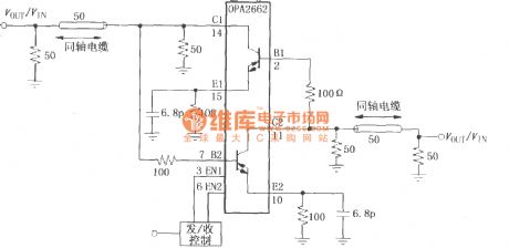
The circuit uses OPA2662 internal dual OTA to form two - channel current output drive circuit, and one channel is used as send driver, the other way is used as receiver driver, sending and receiving switch is controlled by the enable terminal EN. When 3 feet (EN1) is high ( 6 feet EN2 is low at this time), the circuit is in the receiving state, the input signal is sent into 2 feet by cable, then it is amplified and output from 14 feet.
(View)
View full Circuit Diagram | Comments | Reading(1525)
LOG101/104 precision logarithmic and logarithmic ratio amplifier
Published:2012/10/15 22:46:00 Author:Ecco | Keyword: precision logarithmic, logarithmic ratio, amplifier

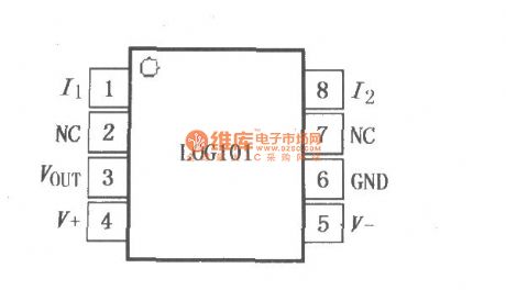
In logarithmic ratio computing applications, a signal current can be from the photodiode, and another reference current is derived from a series resistor of external precision reference. The VOUT terminal's output signal is tuned with the input current decimal 1V, and it allows seven decimal input current dynamic range. LOG101/104 has a low DC offset voltage and low temperature drift characteristics, and it can be used for the measurement of low-level signal in a wide ambient temperature.
(View)
View full Circuit Diagram | Comments | Reading(1328)
Logarithmic transformation function circuit with I1 and I2 being positive( logarithmic amplifier 4127)
Published:2012/10/15 21:52:00 Author:Ecco | Keyword: Logarithmic, transformation function, I1 , I2 , positive, logarithmic amplifier
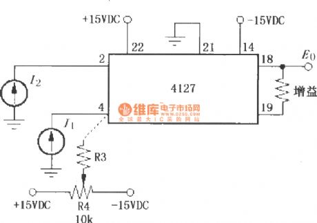
As shown in figure, it is the output logarithmic transformation function circuit with the signal I1 , I2 being positive and input with current form. When the inputs I1 and I2 flow to 4127's 4 feet and 2 feet as the direction shown in figure, they are positive current, the output voltage E0 = - A · log ( I1/I2 ), then output is converted into logarithmic form.
(View)
View full Circuit Diagram | Comments | Reading(779)
Logarithmic transformation function circuit with I1 being negative and I2 being positive( logarithmic amplifier 4127)
Published:2012/10/15 21:57:00 Author:Ecco | Keyword: Logarithmic, transformation function , I1 , negative , I2 , positive, logarithmic amplifier 4127
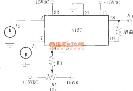
As shown in figure, it is the output logarithmic transformation function circuit with the signal I1 being negative, I2 being positive and input with current form. When the input I1 flows to 4127's 7feet and I2 flows to 2 feet as the directionshown in figure,output voltage E0 = - A · log ( I1/I2 ), then output is converted into logarithmic form.
(View)
View full Circuit Diagram | Comments | Reading(788)
The integrated three pulse trigger components KCZ3 electrical schematic
Published:2012/10/15 22:55:00 Author:Ecco | Keyword: integrated , three pulse, trigger components, electrical schematic
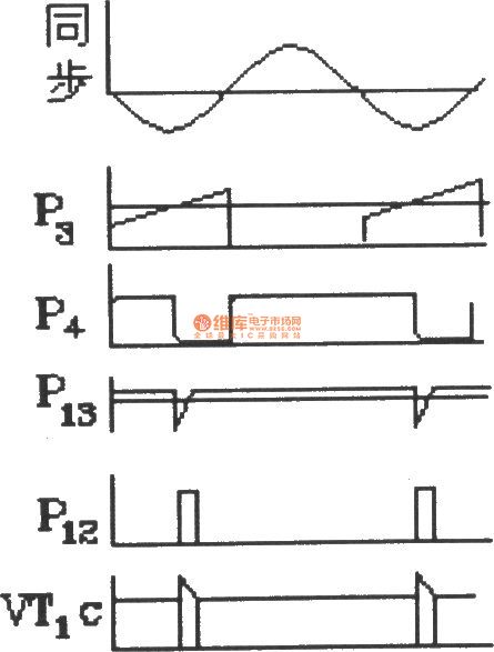
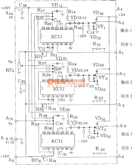
KCZ3 integrated three - pulse triggering component SCR is suitable for three-phase half-bridge inverter trigger. Each phase output pulse can be reliably drive a high-power thyristor, and it can adapt to a variety of phase voltage.The electrical parameters are shown as following:Phase shift control voltage: 0 ~ +8 v ( variable on request).Phase shift range: ≥ l70 .AC synchronization voltage: l0V ( rms) phase voltage. The output stage allowing load current: 300mA.Pulse edge ≤ lμs.Supply Voltage: DC +15 V,-l5V, allow fluctuations of ± 5%.
(View)
View full Circuit Diagram | Comments | Reading(3187)
Two 5:00 LED display driver circuits with HA7666P/TA7667P
Published:2012/10/14 20:22:00 Author:Ecco | Keyword: Two, 5:00, LED display, driver
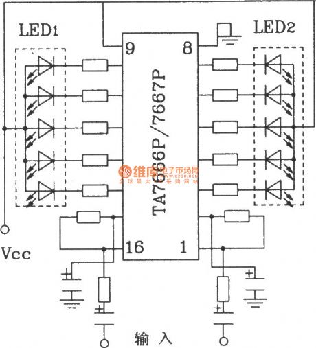
This circuit input signal is analog voltage input, and the scale display can use 10:00 display model TLR8101 or TLG8101.
(View)
View full Circuit Diagram | Comments | Reading(2348)
Two motors starting circuit with autotransformer
Published:2012/10/14 20:27:00 Author:Ecco | Keyword: Two motors , starting , autotransformer
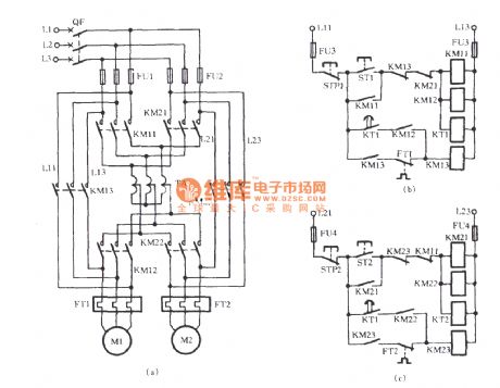
Figure (a) shows the main circuit; Figure (b) is a control circuit of M1 ; Figure (c) is a control circuit of M2. Motor M1 is controlled by KM11, KM12, KM13 and KT1; motor M2 is controlled by KM21, KM22, KM23 and KT2. In order to ensure two electric motors can start at the different time, it is setting the interlock circuit.
(View)
View full Circuit Diagram | Comments | Reading(3585)
Three motors starting circuit using autotransformer
Published:2012/10/14 20:34:00 Author:Ecco | Keyword: Three motors, starting, autotransformer
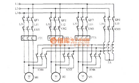

Figure (a)is the switching display circuit for starting three motors; Figure (b) shows a start control circuit of motor M1; Figure ( c ) , ( d )are respectively start control circuit of M2, M3.
(View)
View full Circuit Diagram | Comments | Reading(2507)
The tone control circuit
Published:2012/10/14 21:10:00 Author:Ecco | Keyword: Tone control
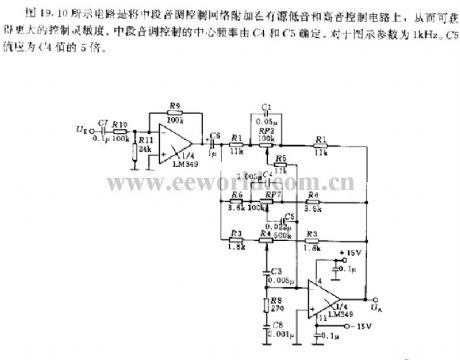
The circuit shown in Figure 19.10 will add the middle tone control network to active bass and treble control circuit, allowing for greater control sensitivity. The middle tone controlling center frequency is determined by C4 and C5. For the icon parameter, it is 1kHz. C5 value should be 5 times of C4 value.
(View)
View full Circuit Diagram | Comments | Reading(2184)
The head and tail distinguished of the motor windings with battery
Published:2012/10/14 21:10:00 Author:Ecco | Keyword: head and tail , distinguished , motor windings , battery
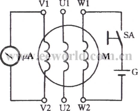
As shown in figure, two queen batteries G are connected with a manual switch SA in series, then they are connected with the head and tail end, and another windings of the motor are connected to a multimeter (mA block). When SA is turned on, the pointer is greater than zero.
(View)
View full Circuit Diagram | Comments | Reading(1107)
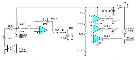
50-Watt Amplifier
Published:2012/10/12 22:53:00 Author:muriel | Keyword: 50-Watt, Amplifier

This is a handy, easy to build general purpose 50 watt amp. The amp has an input for a radio, TV, stereo or other line level device. It also has a phono input for a record player, guitar, microphone or other un-amplified source. With the addition of a low pass filter at the input, it makes a great amp for a small subwoofer. (View)
View full Circuit Diagram | Comments | Reading(1562)
| Pages:302/2234 At 20301302303304305306307308309310311312313314315316317318319320Under 20 |
Circuit Categories
power supply circuit
Amplifier Circuit
Basic Circuit
LED and Light Circuit
Sensor Circuit
Signal Processing
Electrical Equipment Circuit
Control Circuit
Remote Control Circuit
A/D-D/A Converter Circuit
Audio Circuit
Measuring and Test Circuit
Communication Circuit
Computer-Related Circuit
555 Circuit
Automotive Circuit
Repairing Circuit