
Circuit Diagram
Index 358
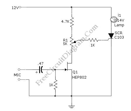
Sound-Activated Lamp (Relay/Switch)
Published:2012/9/3 2:17:00 Author:Ecco | Keyword: Sound-Activated Lamp, Relay, Switch
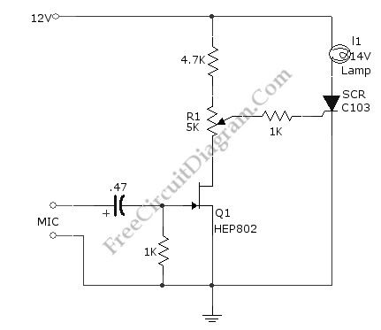
This simple circuit shown int the schematic diagram actives the switch using sound. We can use this circuit for various applications, such as automatic (sound-controlled) disco light or car’s LED light show. The Q1 amplify the audio from mic. The R1 is used to adjust the peak of signal to greater than about 0.7 volts, act as sensitivity adjuster. A certain level, the signal coming from microphone, after amplification by Q1, will trigger the SCR and light lamp I1. If we change the lamp with a relay, then we can get a sound-activated relay/switch, which can be used to control more powerful / high wattage high voltage lamps. If we use a relay, place a 1N4007 diode in parallel with the relay coil to prevent the back-emf from relay coil destroying the SCR. Here is the schematic diagram of the circuit:(Source: freecircuitdiagram)
(View)
View full Circuit Diagram | Comments | Reading(4217)
Telephone Circuit: Music On Hold
Published:2012/9/3 2:16:00 Author:Ecco | Keyword: Telephone, Music On Hold
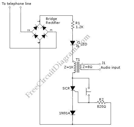
Waiting a call hold can be boring if there is only silence on the line. It’s a good thing to present an “easy music” in call hold, make a long waiting time feels much shorter. This simple circuit (consists of diodes, SCR, and some passive components) allows to place the caller on hold in one room then answer the phone again at another place, or at same phone at later time after doing something. This circuit is called music hold on circuit. This circuit will be turned off automatically when the phone is picked up the second time and the conversation can be continued. Here is the schematic diagram of the circuit: (Source: freecircuitdiagram)
(View)
View full Circuit Diagram | Comments | Reading(3065)
Heartbeat Sensor (Tranduscer)
Published:2012/9/3 2:00:00 Author:Ecco | Keyword: Heartbeat Sensor, Tranduscer
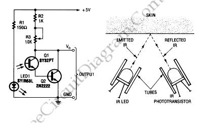
To build a heart-beat transducer not as difficult as imagined. Circuit below shows a simple heart-beat transducer.
This circuit made from an infrared phototransistor and infrared LED. This transducer works with the principle of light reflection,in this case the light is infrared. The skin is used as a reflective surface for infrared light. The density of blood in the skin will affect on the IR reflectivity. The pumping action of heart causes the blood density rises and falls. So that we can calculate the heart rate based on the rise and fall of intensity of infrared that reflected by skin.
Source: freecircuitdiagram
(View)
View full Circuit Diagram | Comments | Reading(2375)
Simple Lie Detector
Published:2012/9/3 1:58:00 Author:Ecco | Keyword: Simple , Lie Detector

Source: freecircuitdiagram
To know someone is lying or not we can use lie detector. This is a simple lie detector that can be made in minutes. It works to detect the someone who telling lie but it is not as sophisticated as the ones the professionals use. Here is the schematic diagram of this circuit:
The skin resistance will go down when someone telling lie and this circuit works by measuring it. We can use electrode pads, alligator clips, or just wires and tape as the electrodes. We have to adjust R2 to position the meter at the center at the beginning of the interrogation (relax condition), then we can know someone is lying when the meter changes in response to a question.
(View)
View full Circuit Diagram | Comments | Reading(0)
Single Cell 1.5V Hearing Aid
Published:2012/9/3 1:57:00 Author:Ecco | Keyword: Single Cell , 1.5V, Hearing Aid

Source: freecircuitdiagram
This circuit can be assembled in a small board, or you can even do it without board. To assemble without board, you can connect every component leads each other and solder them. Align the component bodies and their leads to avoid shorts, secure with insulation tape, glue, or resin.
This is a hearing aid circuit with 1.5v supply. This circuit is used to detect very faint sounds, then deliver the sounds to an 8 ohm earpiece. This circuit requires 1.5v input voltage, need only a single cell battery. Here is the schematic diagram of the circuit:
(View)
View full Circuit Diagram | Comments | Reading(4093)
Direct Coupled Discrete Astable Multivibrator
Published:2012/9/3 1:52:00 Author:Ecco | Keyword: Direct , Coupled, Discrete, Astable Multivibrator
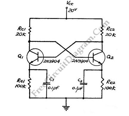
Thisflip-flopcircuitisafreerunning/astablemultivibratorone,withbasesandcollectorofbothemitterbiasedtransistoraredirectlycoupledtoeachother.Switchingactionissupportedbymeansofcapacitorineachemittercircuit.Thisconfigurationproduceatrianglewavesatemitters.Sinceneithertransistorcanremainpermanentlycutoff,thenafreerunningoscillationwillbegenerated.Wecanusesingle0.1uFcapacitorbetweenemittersinplaceofC1andC2. Source:freecircuitdiagram (View)
View full Circuit Diagram | Comments | Reading(1070)
Single Chip Circuit for Multiplication Operation
Published:2012/9/3 1:50:00 Author:Ecco | Keyword: Single Chip , Multiplication Operation
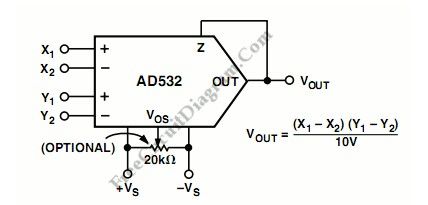
TheAD532shouldbeconnectedasthefollowingfigureforoperationasamultiplier.WecanfedtheinputdifferentiallytotheXandYinputs,orsingleendedbysimplygroundingtheunusedinput.Connecttheinputsaccordingtothedesiredpolarityintheoutput.Toclosethefeedbacklooparoundtheopamp,theZterminalistiedtotheoutput.TheoffsetadjustVosisoptionalandisadjustedwhenbothinputsarezerovoltstoobtainzeroout,ortobuckoutothersystemoffsets. Source:freecircuitdiagram (View)
View full Circuit Diagram | Comments | Reading(580)
AD532 Squarer Circuit
Published:2012/9/3 1:49:00 Author:Ecco | Keyword: Squarer
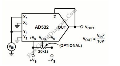
Source:freecircuitdiagram Thefollowingschematicdiagramshowsasquaringcircuit.Basically,thiscircuitisasimplevariationofmultipliercircuit.However,thedifferentialinputcapabilityoftheAD532canbeusedtoobtainapositiveornegativeoutputresponsetotheinput.Thiscircuithasusefulfeaturewhichissuitableforcontrolapplications,asitmighteliminatetheneedforanadditionalinvertersomewhereelse.
(View)
View full Circuit Diagram | Comments | Reading(665)
Single Chip Divider Circuit
Published:2012/9/3 1:47:00 Author:Ecco | Keyword: Single Chip , Divider
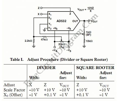
Source: freecircuitdiagram
We can build a divider circuit using only a single chip component, a special purpose integrated circuit AD532. We can configure the AD532 as a two quadrant divider by connecting the multiplier cell in the feedback loop of the op amp and using the Z terminal as a signal input, as shown in the following figure. For your note, the output error is given approximately by 10 Vεm/ (X1-X2), where εm is the total error specification for the multiply mode and bandwidth by fm x (X1-X2)/10 V, where fm is the bandwidth of the multiplier. The X input is restricted to negative values to avoid positive feedback. Thus, connect the input to X and the offset null to X2 for single ended negative inputs. For single ended positive inputs (0V to +10V), connect the input to X2 and the offset null to X1. Gain (S.F) and offset (X0) adjustment are recommended as shown and explained in the following table for optimum performance. The useful range in denominator input is approximately 500 mV ≤ (X1-X2) ≤ 10 V for practical reason. If used, the voltage offset adjust (Vos) is trimmed with Z at zero and (X1-X2) at full scale.
(View)
View full Circuit Diagram | Comments | Reading(651)
Basic Logic Gate with PNP Transistor
Published:2012/9/3 1:46:00 Author:Ecco | Keyword: Basic , Logic Gate , PNP Transistor
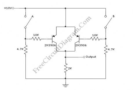
Source: freecircuitdiagram
This schematic diagram shows a circuit of basic logic gate circuit. This PNP transistor circuit can act as OR gate or AND gate. If the input is closing of switch, this circuit acts as AND gate. This circuit acts as OR gate when the input is opening of switch. The phase inversion of input does not complicate overall circuitry. Here is the schematic diagram of the circuit:
(View)
View full Circuit Diagram | Comments | Reading(1460)
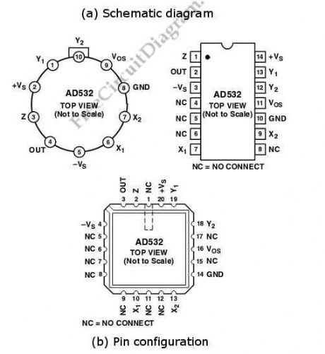
Phase-Sensitive Sinusoidal Signals Detector
Published:2012/9/3 1:44:00 Author:Ecco | Keyword: Phase-Sensitive, Sinusoidal Signals, Detector

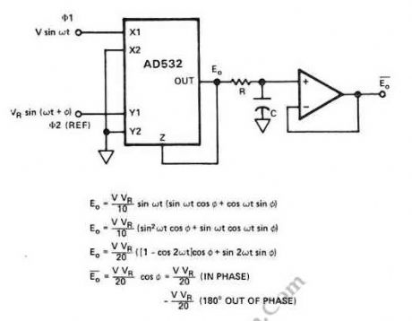
Source: freecircuitdiagram
Using the phase sensitive detector circuit below the magnitude of sinusoidal signal can be measured. Beside that, this circuit also can be used to measures 180°-out-of-phase inputs with proper polarity. But, it depends on the relationship to the reference with less than 1% error. This circuit uses a AD741J op amp. Here is the schematic diagram of the circuit and the pin configuration of AD532:
(View)
View full Circuit Diagram | Comments | Reading(1910)
Square Root Mode for AD532 Analog Processor
Published:2012/9/3 1:42:00 Author:Ecco | Keyword: Square Root Mode, Analog Processor
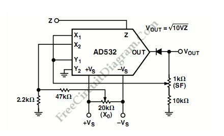
Source: freecircuitdiagram
The following schematic diagram shows us about the connections for square root mode for ADS532 analog processor chip. Similar to the division mode, the multiplier cell is connected in the feedback of the op amp by connecting the output back to both the X and Y inputs. To prevent latch up as Zi approaches 0 Volts, the diode D1 is connected. The Vov adjustment is made with Zin = +0.1 V dc in this case, adjusting Vos to obtain -1.0 V dc in the output, Vout =-√(10 VZ). Gain (S.F) and offset (Xo) adjustments are recommended for optimum performance.
(View)
View full Circuit Diagram | Comments | Reading(1577)
Difference Of Squares Analog Computing
Published:2012/9/3 1:40:00 Author:Ecco | Keyword: Difference , Squares Analog Computing
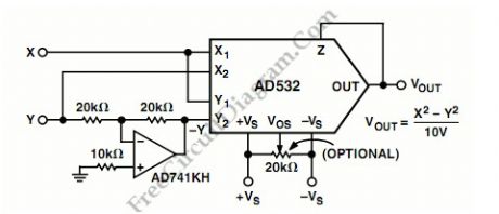
Source: freecircuitdiagram
Because the differential input capability of the AD532, algebraic solution of several interesting functions such as difference of squares, (X2-Y2)/10V is allowed. The following figure shows us about the configuration of AD532 in the square mode, with a simple unity gain inverter connected between one of the signal inputs (Y) and one of the inverting input terminals (-Yin) of the amplifier. For unity gain and best accuracy, the inverter should use precision (0.1%) resistors or be otherwise trimmed.
(View)
View full Circuit Diagram | Comments | Reading(665)
Analog Multiplier-Divider with 4136 Op-Amps
Published:2012/9/3 1:39:00 Author:Ecco | Keyword: Analog Multiplier-Divider, Op-Amps
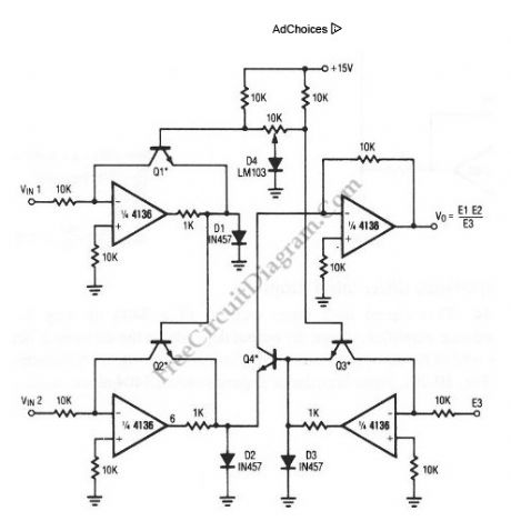
Source: freecircuitdiagram
This unique circuit below can be used as divider and multiplier. This circuit is formed by all four sections of a 4136 . The Q1 through Q4 can be any PNP transistor, but that must matched transistors. The transistor matching determine the acurracy of the divider and multiplier circuit. Here is the schematic diagram of the circuit:
(View)
View full Circuit Diagram | Comments | Reading(4233)
Wien-Bridge Oscillator Using HA2541 Op-Amp
Published:2012/9/3 1:38:00 Author:Ecco | Keyword: Wien-Bridge, Oscillator , Op-Amp
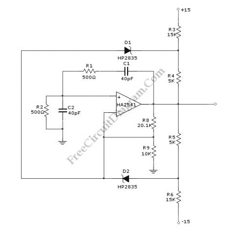
Source: freecircuitdiagram
A Wien-Bridge oscillator circuit can be built from HA2541 and some basic components. This circuit can generate good-quality sine wave of 40 MHz with an upper limit of 50 MHz. The R3 through R7 and D2 and D1 provide the diode limiting for this circuit. Here is the schematic diagram of this circuit:
(View)
View full Circuit Diagram | Comments | Reading(1313)
True Stereo Indicator Detects L-R Signal Difference
Published:2012/9/3 1:32:00 Author:Ecco | Keyword: True , Stereo , Indicator, Detects , L-R Signal Difference
Source: freecircuitdiagram
This true stereo indicator is different from what we usually find on FM radio receiver, which is usually a pilot tone detector. A stereo broadcast from FM radio station contain pilot tone, but a presence of pilot tone doesn’t necessarily a stereo broadcast signal since a mono FM transmitter ca broadcast pilot tone as well. Since this circuit detect the difference between left and right channel, this circuit can detect a real stereophonic programs. When there is no difference between R and L input signals, the output A1 and output A2 is at the same potential. That will make a a virtual ground rail at half the supply voltage. Here is the schematic diagram of the circuit:
(View)
View full Circuit Diagram | Comments | Reading(1434)
Discrete Sliding Tone (Frequency Ramp) Doorbell
Published:2012/9/3 1:31:00 Author:Ecco | Keyword: Discrete Sliding Tone , Frequency Ramp, Doorbell

Source: freecircuitdiagram
This doorbell circuit produces a low tone that will slide up to higher frequency. The equivalent total resistance connected between the base of Q1 and ground (Rbg) , and coupling capacitor C1 determines the AF oscillator’s frequency. The resistance (Rbg) is equal to (R2+R1)R3. Here is the schematic diagram of the circuit:
(View)
View full Circuit Diagram | Comments | Reading(1097)
TDA7056 3W BTL Mono Audio Power Amplifier
Published:2012/9/3 1:27:00 Author:Ecco | Keyword: 3W , BTL , Mono , Audio , Power Amplifier
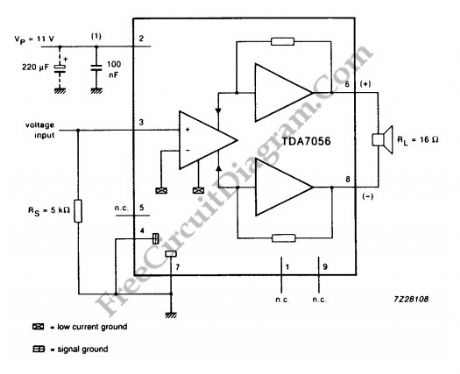
Source: freecircuitdiagram
For mono output amplifier application, TDA7056 IC can be your option. Compact but powerful, this integrated circuit is contained in a 9 pin medium power package. This device is designed for battery fed portable equipments such as mono recorders, radios and television. To attract the market, TDA7056 has many features such as low power consumption. For more reliable operation, TDA7056 also has short circuit proof and ESD (Electro Static Discharge) protected on all pins. Designing application with this IC should be easy since no external components is needed. To make sure you’ll love this chip, this device also has no switch on/off clicks. Overall, TDA7056 has good stability.
(View)
View full Circuit Diagram | Comments | Reading(2709)
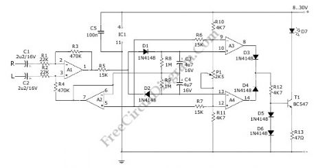
Compressor Circuit with 570/571 Compandor IC
Published:2012/9/3 1:26:00 Author:Ecco | Keyword: Compressor, Compandor IC
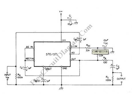
Source: freecircuitdiagram
Compressor circuit provide high gain for low amplitude input and provide low gain for high amplitude input. This action, in effect, produce a nearly constant amplitude even though the input has very high dynamic range (very high amplitude variation from time to time). The action of compression like this is needed in some situation, such as in maximizing modulation depth in broadcasting, or sustaining electric guitar signal which has very high variation between the plucking time and fading out. The following circuit has complementary input/output characteristic and unity gain at 0.775 VRMS input. Voltage gain through compressor is square root of 0.7/Vin. Vin is average input voltage. This circuit uses Signetics dual channel compandor IC. 570 has lower inherent distortion and higher supply voltage range (6-24 V) than 571 (6-18 V).
(View)
View full Circuit Diagram | Comments | Reading(2747)
Sound-Activated Lamp (Relay/Switch)
Published:2012/9/3 1:24:00 Author:Ecco | Keyword: Sound-Activated Lamp , Relay, Switch
Source: freecircuitdiagram
This simple circuit shown int the schematic diagram actives the switch using sound. We can use this circuit for various applications, such as automatic (sound-controlled) disco light or car’s LED light show. The Q1 amplify the audio from mic. The R1 is used to adjust the peak of signal to greater than about 0.7 volts, act as sensitivity adjuster. A certain level, the signal coming from microphone, after amplification by Q1, will trigger the SCR and light lamp I1. If we change the lamp with a relay, then we can get a sound-activated relay/switch, which can be used to control more powerful / high wattage high voltage lamps. If we use a relay, place a 1N4007 diode in parallel with the relay coil to prevent the back-emf from relay coil destroying the SCR. Here is the schematic diagram of the circuit:
(View)
View full Circuit Diagram | Comments | Reading(0)
| Pages:358/2234 At 20341342343344345346347348349350351352353354355356357358359360Under 20 |
Circuit Categories
power supply circuit
Amplifier Circuit
Basic Circuit
LED and Light Circuit
Sensor Circuit
Signal Processing
Electrical Equipment Circuit
Control Circuit
Remote Control Circuit
A/D-D/A Converter Circuit
Audio Circuit
Measuring and Test Circuit
Communication Circuit
Computer-Related Circuit
555 Circuit
Automotive Circuit
Repairing Circuit