
Circuit Diagram
Index 359
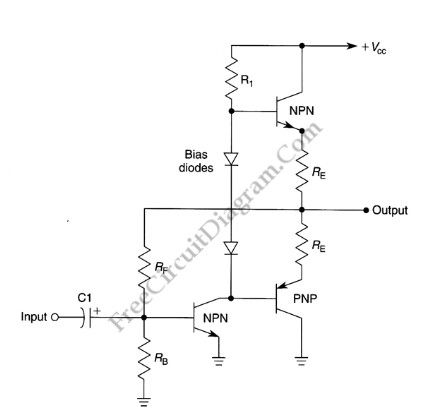
Basic Complementary (Push-Pull) Power Amplifier Circuit
Published:2012/9/3 1:19:00 Author:Ecco | Keyword: Basic Complementary, Push-Pull, Power Amplifier
Source: freecircuitdiagram
This amplifier circuit is very popular audio power amplifier circuit type. We call it a complementary since the final transistors is an NPN-PNP pair, each with the same characteristics. This circuit produce an AB class amplifier, since each transistor works in slightly more than half cycle of the signal. There is overlap area when both transistor conduct a current, and this area will be around its stationary current (when the input signal is zero). This circuit is also known as push-pull amplifier circuit since each transistor in the pair is working alternatively. Here is the schematic diagram of the circuit:
(View)
View full Circuit Diagram | Comments | Reading(2680)
Voltage-Controlled Attenuator (Volume Control) Using FET
Published:2012/9/3 1:16:00 Author:Ecco | Keyword: Voltage-Controlled Attenuator , Volume Control, FET
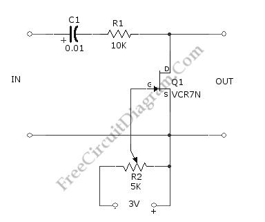

Using the circuit shown in the schematic diagram below, we can control the low-level audio signals with ±3V variable DC voltage. This attenuator circuit uses a field effect transistor (FET) to shunt the signal to ground. The R2 is used to control the output level (the attenuation level), but you can use other source of voltage signal to control the grid of the FET, such as DAC output, just remember that this voltage is a negative going signal (you can use with DAC which uses symmetric power supply system). The minimum output of this circuit is when gate bias is zero. When the gate bias is set close to pinchoff value, the circuit will produce maximum output with value that equal to input level. Here is the schematic diagram of the circuit:
Source: freecircuitdiagram (View)
View full Circuit Diagram | Comments | Reading(4685)
60-dB Range Compressor For Audio
Published:2012/9/3 1:13:00 Author:Ecco | Keyword: 60-dB Range, Compressor , Audio
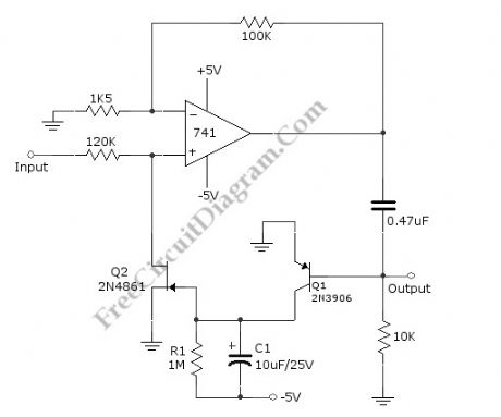
A compressor circuit shown in the schematic diagram below can produce consistent output of 1.4V P-P over entire 60dB range that is very useful for audio level/volume stabilization. As the main components, this circuit uses a 741 opamp and JFET. With input range of 20mV to 2oV, this circuit has delay time of 0.4s (decay time) and response time of 1.2ms (attack time). The JFET is used as voltage-controlled resistor in peak-detecting control loop of 741 opamp. Here is the schematic diagram of the circuit:
source: freecircuitdiagram (View)
View full Circuit Diagram | Comments | Reading(3431)
Telephone Circuit: Music On Hold
Published:2012/9/3 1:09:00 Author:Ecco | Keyword: Telephone , Music On Hold
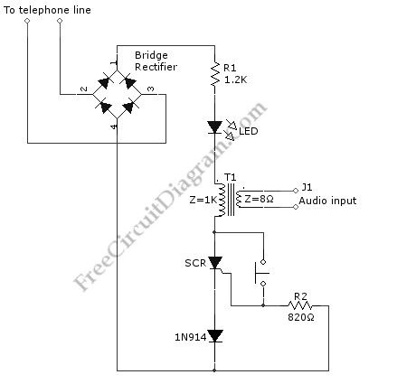
Waiting a call hold can be boring if there is only silence on the line. It’s a good thing to present an “easy music” in call hold, make a long waiting time feels much shorter. This simple circuit (consists of diodes, SCR, and some passive components) allows to place the caller on hold in one room then answer the phone again at another place, or at same phone at later time after doing something. This circuit is called music hold on circuit. This circuit will be turned off automatically when the phone is picked up the second time and the conversation can be continued. Here is the schematic diagram of the circuit:
Source: freecircuitdiagram (View)
View full Circuit Diagram | Comments | Reading(1)
Loud 10-W Car Alarm Siren
Published:2012/9/3 1:07:00 Author:Ecco | Keyword: Loud, 10-W, Car Alarm Siren

By generating square-wave output that sweeps down and up in frequency, this circuit can produce force field of high-intensity sound inside car. This circuit can make a car thieve panics and decide to run before anyone catch his action. D1, C1 and R1 produce triangle waveform by shaping a square wave output of IC1. If using sweeping alarm sound is prohibited by regulation, then C1 can be removed to provide legal two-tone sound. The diodes are general purpose small signal silicon except D2 which is silicon rectifier rated 1 A at 50 PIV. This circuit can handle up to 10W depends on the horn loudspeaker. Here is the schematic diagram of the circuit:
(View)
View full Circuit Diagram | Comments | Reading(2066)
Direct driving capacitive input high-speed A/D converter circuit diagram with INA155/156
Published:2012/8/30 1:42:00 Author:Ecco | Keyword: Direct driving , capacitive input , high-speed A/D converter
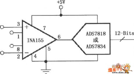
In the figure, G = 10. Input voltage is sent to 12-bit high-speed low-power sampling A / D converter ADS7818 or ADS7834 after being amplified by INA155. The internal input terminal of ADS7818 or ADS7834 is the capacitor array (CDAC), namely the capacitive input, and A / D converter converts the input analog signal to 12-bit digital signal output, fSAMPLE = 500kHz.
(View)
View full Circuit Diagram | Comments | Reading(797)
Phase adjustable circuit diagram
Published:2012/8/29 21:30:00 Author:Ecco | Keyword: Phase adjustable
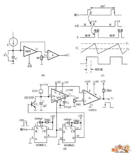
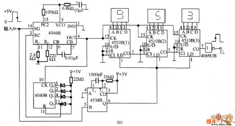
In the diagram (a), it is a phase adjustable circuit with digital set composed of PLL IC, and the PLL IC 4046B and divider 4040B form the circuit with output signal frequency being 360 times of the input signal frequency, and the following is counter 451OB with the digital switch so that the phase change between 0 ~ 360°. The circuit's operating frequency range is from several tens to several hundreds Hz the phase is 0 ~ 360 °, and the resolution is 1 °. The drawback of the circuit is slow to respond, and needs to be set with digit.
Figure (b) shows circuit scheme, FIG (c ) is an operation timing diagram. In the diagram (b), the current flowscapacitor C to become the constant current IC, then the voltage Uc on C raises like the straight line shown in (c).
(View)
View full Circuit Diagram | Comments | Reading(2064)
Active low-pass filter circuit diagram
Published:2012/8/29 21:18:00 Author:Ecco | Keyword: Active low-pass filter
View full Circuit Diagram | Comments | Reading(1422)
Celsius thermometer circuit diagram with AD594
Published:2012/8/29 21:18:00 Author:Ecco | Keyword: Celsius thermometer

AD594/595 can also be configured to the Celsius thermometer, and the circuit is shown as the figure. The IN + and IN - ends should be connected with COM in short circuit, the temperature coefficient of the output voltage Uo is 10mV / ℃, and it can be served in the DVM to measure and display the temperature value.
(View)
View full Circuit Diagram | Comments | Reading(1676)
The MOS FET inverter circuit diagram of power transformer
Published:2012/8/30 1:51:00 Author:Ecco | Keyword: MOS, FET, inverter , power transformer
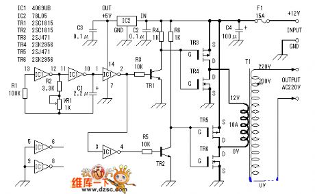
It mainly consists of MOS FET, ordinary power transformer. Its output power depends on the power of MOS FET and power transformer. It has no the cumbersome transformer winding, so it is suitable for the amateur production of electronics enthusiasts.
(View)
View full Circuit Diagram | Comments | Reading(2359)
Text-display logic pen (CD4011) circuit diagram composed of gate circuit
Published:2012/8/30 1:56:00 Author:Ecco | Keyword: Text-display , logic pen, gate
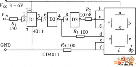
Text-display logic pen with gate circuit can take many forms, and it can be composed of inverters, also can be composed of NAND gate or NOR gate. As shown in the figure, the logic pen consists of NAND gate CD4011 and common anode digital tube.
(View)
View full Circuit Diagram | Comments | Reading(4123)
Voice-activated music coloured light circuit (2)
Published:2012/8/29 22:54:00 Author:Ecco | Keyword: Voice-activated , music , coloured light
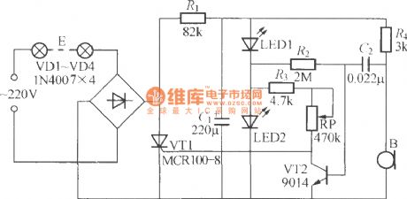
As shown in the figure, it is a modified voice-activated music coloured light. (1) It uses bridge full wave circuit, and the current flowing through Lantern series is full wave pulsating current, so the brightness of Lantern series is improved; (2) It uses LED1 and LED2 for power supply, and it can get stable DC voltage from two ends of LED, while LED also can be used for power indicator; (3) The sound-electric transducer uses electret capacitance microphone to effectively improve Sonic controlling sensitivity.
(View)
View full Circuit Diagram | Comments | Reading(1516)
Voice-activated music coloured light circuit (1)
Published:2012/8/29 22:43:00 Author:Ecco | Keyword: Voice-activated, music , coloured light

Voice-activated music coloured light does not require any wire connections with audio equipment, and it directly uses the acoustic control to make the lights flash with the music played by speakers, it is very easy to use, its circuit is shown as the figure. RP can be used to adjust the sound control sensitivity.
(View)
View full Circuit Diagram | Comments | Reading(1631)
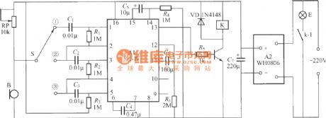
Voice-activated delayed light switch circuit (3)
Published:2012/8/29 22:33:00 Author:Ecco | Keyword: Voice-activated , delayed light, switch
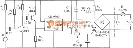
As shown in the figure, it is a voice-activated delayed light with music doorbell chip voice as the core component, when it is used, blowing whistle or filming palm, the lights will be lit with delayed around 20s, then the light will go off automatically, so it makes life easier. Another feature of the circuit is that it uses two-wire connection, you can directly replace the normal switch without changing the original indoor circuit; it can also connects to an ordinary light switch in parallel, then the common light is retrofited into voice-activated delayed light. The lighting time length depends on the length of music signals storaged in doorbell chip, KD-9300 integrated circuit signal depends on the storaging music, it is usually 10~20s.
(View)
View full Circuit Diagram | Comments | Reading(1508)
Voice-activated delayed light switch circuit (2)
Published:2012/8/29 22:36:00 Author:Ecco | Keyword: Voice-activated , delayed light, switch

As shown in the figure, itis a voice-activated delayed light switch circuit with strong anti-jamming ability, it needs to strike hands three times in a specified time, then thelight will be lit, after delayed for some time, the light wii be automatically turned off. The delayed time of circuit is decided by C3, when C3 is 10μF, the delayed time is about 5s; when C3 is 47μF, the delayed time is about 15s; when C3 is 100μF, the delayed time is about 40s.
(View)
View full Circuit Diagram | Comments | Reading(2161)
Voice-activated delayed light switch circuit (1)
Published:2012/8/29 22:13:00 Author:Ecco | Keyword: Voice-activated, delayed light, switch
As shown in the figure, itis a voice-activated delayed light switch circuit with strong anti-jamming ability, it needs to strike hands three times in a specified time, then thelight will be lit, after delayed for some time, the light wii be automatically turned off.
(View)
View full Circuit Diagram | Comments | Reading(1532)
Two -phase oscillator circuit diagram
Published:2012/8/30 1:47:00 Author:Ecco | Keyword: Two -phase oscillator
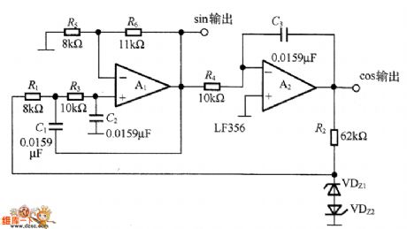
In the circuit, it is composed of op-amps A1 and A2, etc., and the op-amp A1 is a low-pass filter, A2 is an integrator, and each phase lag 90 °, the total phase lag is 180 °. The oscillation frequency is determined by R1 + R2, R3, R4 , C1, and C2, and C3. According to the parameters of FIG, the oscillation frequency is 1 kHz. The regulator tubes VDz1 VDz2 are mainly used to stabilize the amplitude, but in order to reduce the distortion of the waveform, it must choose two regulators with the same characteristics. The distortion of the cosine (cos) output waveform in the circuit is controlled at 0.3% or less, and the distortion of sine (sin) output waveform is about 1%.
(View)
View full Circuit Diagram | Comments | Reading(1516)
Color changing flashlight circuit diagram
Published:2012/8/29 22:07:00 Author:Ecco | Keyword: Color changing , flashlight
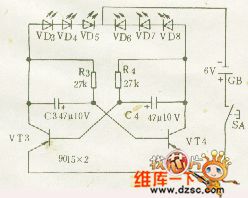
Multivibrator's two transistor collectors are connected to LED respectively, LED can flash alternately accoring to the cycles of multivibrator, this circuit is widely used such as home decorating. This circuit uses high-gain PNP germanium VT3,VT4 to form a multivibrator, there are two inverters are connected with beginning and end, and interstage uses capacitors C3,C4 for coupling, its working cycle is 1S. Transistor should choose the 9012 or 9015 with collecting electrode electric current being greater than 50mA, emitting tube should choose high-brightness tubes. If you want to change the flashing speed, you can adjust the capacity of C3,C4, or fine tune R3,R4 to change the corresponding resistance.
(View)
View full Circuit Diagram | Comments | Reading(1610)
Oscillator circuit diagram with triangle-wave/square wave output
Published:2012/8/30 1:29:00 Author:Ecco | Keyword: Oscillator, triangle wave, square wave
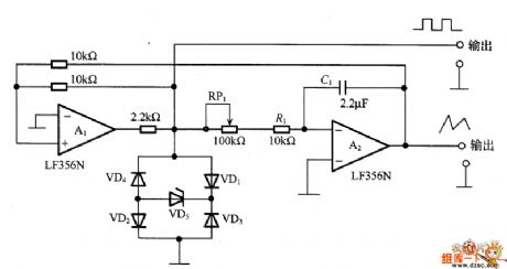
The circuit is composed of lag comparator with A1 and inverting integrator A2, and the charging and discharging time constant is decided by integral resistors (R1+RP1) and the capacitor C1. VD1~VD5 form the limiter circuit. The maximum oscillation frequency is related to swicthing rate of amplifier, when swicthing rate is 10V/μ s, in order to get the 20V (peak-peak) triangle wave, it must have at least 2 μ s lag, even up to 20 μ s, therefore, in order to increase the frequency of oscillation, A1 and A2 should select high speed operational amplifier.
(View)
View full Circuit Diagram | Comments | Reading(3113)
Transmitter circuit diagram with lacking of Harmonic and frequency to 200MHZ
Published:2012/8/29 22:08:00 Author:Ecco | Keyword: Transmitter , lacking , Harmonic , frequency to 200MHZ
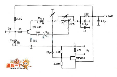
View full Circuit Diagram | Comments | Reading(795)
| Pages:359/2234 At 20341342343344345346347348349350351352353354355356357358359360Under 20 |
Circuit Categories
power supply circuit
Amplifier Circuit
Basic Circuit
LED and Light Circuit
Sensor Circuit
Signal Processing
Electrical Equipment Circuit
Control Circuit
Remote Control Circuit
A/D-D/A Converter Circuit
Audio Circuit
Measuring and Test Circuit
Communication Circuit
Computer-Related Circuit
555 Circuit
Automotive Circuit
Repairing Circuit