
Circuit Diagram
Index 965
60_W_LINEAR_FOR_432_MHz
Published:2009/7/8 3:11:00 Author:May
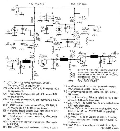
Suitable for mak-ing DX contacts through Oscar satellite, as well as for tropo and local contacts, using CW or SSB. Motorola MRF5176 transistor provides drive to MRF306 output stage, giving sufficient output over range of 430-450 MHz. Requires 1-3 W RF input. Microstrip conductors W1-W3, each 0.077 wavelength long, provide wideband matching and high efficiency. Article gives dimensioned layout for printed-circuit board and all construction details.-J. Buscemi, A 60-Watt Solid-State UHF Linear Amplifier, QST, July 1977, p 42-45. (View)
View full Circuit Diagram | Comments | Reading(731)
Constant_current_motor_drive
Published:2009/7/21 7:34:00 Author:Jessie
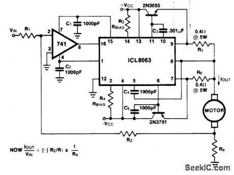
Constant-current motor drive. All capacitors should be at least 50 working volts and resistors the half-watt type, except those valued at 0.4 ohm and Ra. Use heat sinks for the power transistors with thermal compound. This circuit can be used where there is some likelihood of stalling or lockup, If the motor locks the current drive remains constant and the system does not destroy itself (courtesy Intersil, Inc.). (View)
View full Circuit Diagram | Comments | Reading(829)
EMI_FREE_PHASE_CONTROL_OF_HEATER
Published:2009/7/8 3:08:00 Author:May
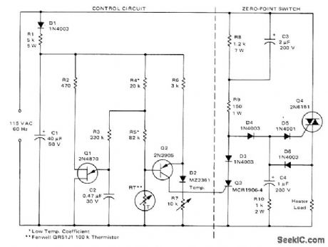
Modulated triac zero-point switch eliminates electromagnetic interference generated by phase control while providing proportional ON/ OFF switching for accurate temperature regulation of heater load. Circuit at right of dashed line is basic zero-point switch that tums triac on almost immediately after each zero crossing between half-cycles. R7 is set so bridge in control circuit is balanced at desired temperature.When temperature overshoots, thermistor RT decreases in resistance and Q2 tums on to providegate drivefor SCR Q3. Q3 then tums on and shunts gate signal away from triac Q4, to remove power from load. When temperature drops, Q2 and Q3 tum off and full-wave power is applied to load. Modulation is achieved by supelimposing sawtooth voltage from Q1 on one arm of bridge through R3, With sawtooth period equal to 12 cycles ol line frequency. From 1 to 12 of these cycles can be applied to load for modulating power in 8% steps from 0% to 100% duty cycle.- Circuit Applications for the Triac, Motorola, Phoenix, AZ, 1971, AN-466, p 13. (View)
View full Circuit Diagram | Comments | Reading(781)
45_MHz_TV_sound_channel_with_audio_output_stages
Published:2009/7/21 7:11:00 Author:Jessie
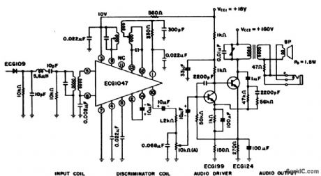
4.5 MHz TV sound channel with audio output stages. The ECG1047 has a three-stage differential amplifier for the IF amplifier section, a ratio detector and first and second audio amplifiers. The IF transformer, ratio detector coil and audio output transformer are standard and can be purchased at Radio Shack. This circuit provides 1.5 watts of audio power into an 8-ohm load (courtesy GTE Sylvania Incorporated). (View)
View full Circuit Diagram | Comments | Reading(1609)
0000075℃_BATH_CONTROL
Published:2009/7/8 3:03:00 Author:May
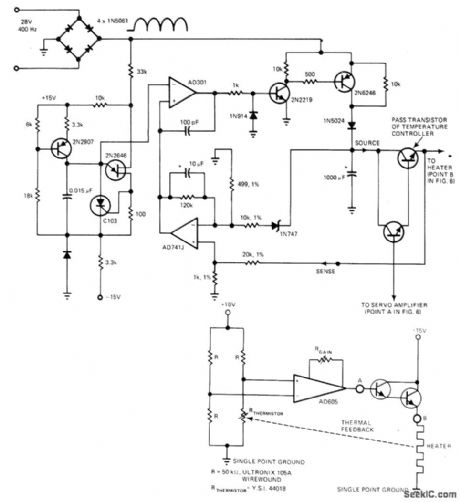
Will hold oven or bath at 37.5 ℃ with high stability. Bridge offset is sensed by AD605 instrumentation opamp having high common-mode rejection, low drift, and balanced inputs. Opamp drives Darlington pair providing current gain to heater. Pass transistor must dissipate all power not delivered to heater; to overcome this, large servo circuit is connected between points A and B to maintain constant 3 V across pass transistor regardless of heater power demands. Output of 741 opamp is compared with 400-Hz line-synchronized ramp by AD301A amplifier serving as pulse-width modulator that drives 2N2219-2N6246 transistor switch. Switch delivers phase-con-trolled power to 100-μF integrating capacitor and pass transistor of temperature controller.-J. Williams, Designer's Guide to: Temperature Control, EDNMagazine, June 20, 1977, p 87-95. (View)
View full Circuit Diagram | Comments | Reading(893)
PARALLEL_TRANSISTOR_OUTPUT_STAGE_WITH_EMITTER_TUNING
Published:2009/7/21 7:07:00 Author:Jessie

Variable capacitor common to both emitters, together with r-f choke for d-c path, Provides efficient tuning and increased power gain at outputs near maximum of 2 w. Chief drawback is reduced Power gain at low input levels,-W.A. Rheinfelder, choosing the Best Transmitter Output Stage,EEE,11:10,p 48-53. (View)
View full Circuit Diagram | Comments | Reading(841)
THREE_MINUTE_TIMER
Published:2009/7/8 3:02:00 Author:May
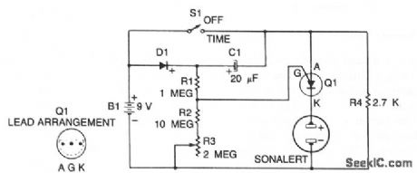
When S1 is off, C1 charges to within 0.5 V of the battery voltage through diode D1 and resistor R4. When S1 is closed, the anode of the PUT rises to the positive supply voltage. The PUT does not conduct, because battery voltage appears in series with the charge stored on C1, which raises the gate of the PUT to a level positive with respect to the anode. The timer relies on the discharge of capacitor C1 through resistors R1, R2, R3,and R4. Once C1 is at zero volts, the PUT will turn on battery voltage to the Sonalert and cause it to sound. (View)
View full Circuit Diagram | Comments | Reading(858)
75℃_CRYSTAL_OVEN
Published:2009/7/8 2:59:00 Author:May
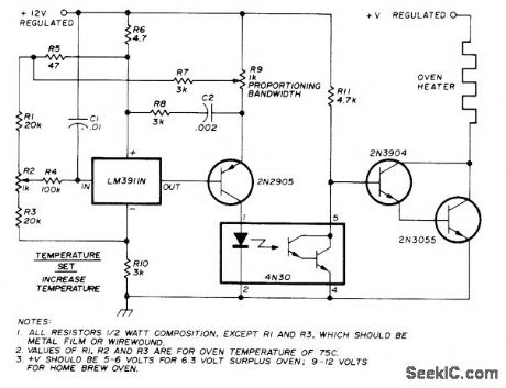
Proportional temperature controller using National LM3911 IC holds crystal oven temperature constant within 0.1℃ of 75 ℃, to improve stability of oscillator used in frequency synthesizers and digital counters.Duty cycle of square-wave output of IC (ratio of OFF to ON time) varies with temperature of sensol in IC and with voltage at inverting input ter-minal. Duty cycle change makes average heater current change as required to bring temperature back to desired value. Square-wave frequency is determined by R4 and C1. 4N30 optocoupler drives power transistor having oven heater in collector circuit. During ON intervals of square wave, power transistor is driven to saturation, and during OFF intervals is cut off.-F. Schmidt, Precision Temperature Control for Crystal Ovens, Ham Radio, Feb. 1978, p 34-37.
(View)
View full Circuit Diagram | Comments | Reading(1599)
COUPLING_TO_HIGH_IMPEDANCE_DETECTOR
Published:2009/7/8 2:58:00 Author:May
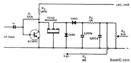
Final IF stage of receiver uses piezoelectric overtone resonator connected backwards for coupling to high-impedance detector. Arrangement provides useful voltage step-up as well, about 2.5 times. Resonator can be Brush Clevite Transfilter.-G. W. Short, Reversed Operation of Transfilter,' Wireless World, Aug. 1971, p 386. (View)
View full Circuit Diagram | Comments | Reading(639)
10_W_AT_50_MC
Published:2009/7/21 7:06:00 Author:Jessie
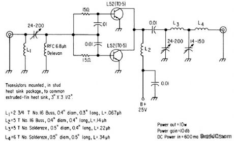
Two L52's in parallel provide 10 w output power with 10 db gain. Separate biasing resistors are used in base circuits to balance operating currents. Input and output impedances are both 50 ohms, and overall efficiency is 65%.-Texos Instruments Inc., Solid-State Communications, McGraw-Hill, N.Y., 1966, p 323. (View)
View full Circuit Diagram | Comments | Reading(682)
ONE_SHOT_TIMER
Published:2009/7/8 2:58:00 Author:May
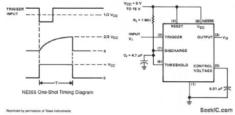
This simple circuit consists of only two timing components RTand CT, the NE555, and bypass capacitor C2. While not essential for operation, C2 is recommended for noise immunity. During standby, the trigger input terminal is held higher than 1/3 VCC and the output is low. When a trigger pulse appears with a level less than 1/3 VCC, the timer is triggered and the timing cycle starts. The output rises to a high level near VCC, and at the same time, CT begins to charge toward VCC. When the CT vottage crosses 2/3 VCC, the timing period ends with the output falling to zero, and the circuit is ready for another input trigger. Because of the internal latching mechanism, the timer will always time out when triggered, regardless of any subsequent noise, such as bounce, on the trigger input. For this reason, the circuit can also be used as a bounceless switch by using a shorter rc time constant. A 100-KΩ resistor for RT and a 1-μF capacitor for CT would give a clean, 0.1 s output pulse when used as a bounceless switch. (View)
View full Circuit Diagram | Comments | Reading(933)
455_kHz_SECOND_IF_
Published:2009/7/8 2:54:00 Author:May
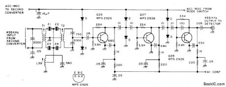
Used in all-band doubleconversion superheterodyne receiver for AM,narrow-band FM, CW, and SSB operation. Input is fed through 455-kHz ceramic filter to highgain amplifier using three MPS 2926 transistors all having automatic gain control and master gain control. Use of silicon rectifiers in interstage networks of IF amplifier gives economical wide-range AGC circuit Supρlγ;is13.6 V regulated Article gives all circuits of receiver.-DM.Eisenberg,Build This All-Band VHF Receiver,73 Magazine,Jan 1975,p 105-112. (View)
View full Circuit Diagram | Comments | Reading(6561)
LONG_TIME_TIMER
Published:2009/7/8 2:49:00 Author:May
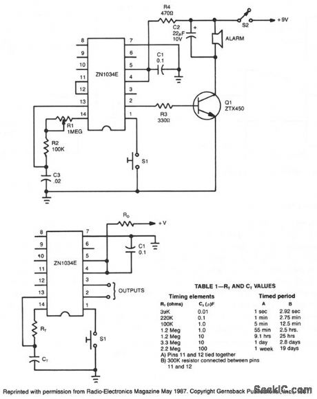
When used as a stand-alone device, ZN1034E from Ferranti can provide timed intervals ranging from 1 second to 19 days, although the rc time constant is only 220 seconds. The ZN1034E includes an internal voltage regulator, an oscillator, and a 12-stage binary counter. The total delay time prodded by the counter is 4095 times the oscillator period. The control logic times-out after 4095 cycles of the oscillator, and delivers high and low output pulses at pins 2 and 3. The output at pin 3 is normally high and decreases at the end of the timed interval. The complementary output at pin 2 is normally low and becomes high at the end of the timed interval. The timing period is initiated by momentarily grounding pin 1. Timing resistor RT consists of two resistors, R1 and R2, in series. Because R1 has a fixed value of 100 KO, the total range of ;RT 100 K to 1.1 MΩ. (View)
View full Circuit Diagram | Comments | Reading(1755)
CMOS_PRECISION_PROGRAMMABLE_LABORATORY_TIMER
Published:2009/7/8 2:38:00 Author:May
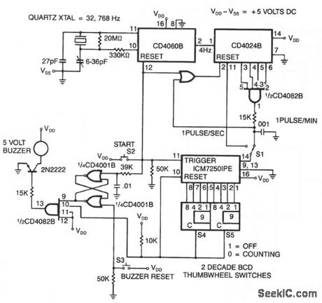
The time base is ftrst selected with S1 set for seconds or minutes, then units 0-99 are selected on the two thumbwheel switches S4 and S5. Finally, switch S2 is depressed to start the timer. Simultaneously, the quartz crystal-controlled divider circuits are reset, the ICM7250 is triggered and counting begins. The ICM7250 counts until the preprogrammed value is reached, then, the value is reset, pin 10 of the CD4082B is enabled, and the buzzer is turned on. Pressing S3 turns the buzzer off. (View)
View full Circuit Diagram | Comments | Reading(1306)
SEQUENTIAL_TIMER
Published:2009/7/8 2:33:00 Author:May
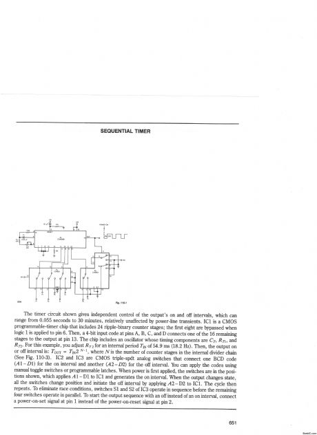
The timer circuit shown gives independent control of the output's on and off intervals, which can range from 0.055 seconds to 30 minutes, relatively unaffected by power-line transients. IC1 is a CMOS programmable-timer chip that includes 24 ripple-binary counter stages; the first eight are bypassed when logic 1 is applied to pin 6. Then, a4-bit input code at pins A, B, C, and D connects one of the 16 remaining stages to the output at pin 13. The chip includes an oscillator whose timing components are CT, RT1, and RT2._For this example, you adjust RT2 for an internal period TlN of 54.9 ms (18.2 Hz). Then, the output on or off interval is: Tour= TIN2 N-1, where N is the number of counter stages in the internal divider chain (See Fig. 110-3). IC2 and IC3 are CMOS triple-spdt analog switches that connect one BCD code (A1 -D1) for the on interval and another (A2-D2) for the off interval. You can apply the codes using manual toggle switches or programmable latches. When power is first applied, the switches are in the positions shown, which applies A1 -D1 to IC1 and generates the on intervat. When the output changes state, all the switches change position and initiate the off interval by applying,42-D2 to IC1. The cycle then repeats. To eliminate race conditions, switches S1 and S2 of IC3 operate in sequence before the remaining four switches operate in parallel. To start the output sequence with an off instead of an on interval, connect a power-on-set signal at pin 1 instead of the power-on-reset signal at pin 2. (View)
View full Circuit Diagram | Comments | Reading(0)
SIMPLE_TIME_DELAY
Published:2009/7/8 2:23:00 Author:May
After the first cycle, the relay will normally be energized. When normally closed pushbutton S1 is activated, the SCR turns off, the relay is de-energized, and power is applied to the relaxation oscilla-tor and the load. After a time delay varying from less than a second to approximately 2.5 minutes, as determined by the setting of the 10-MΩ potentiom-eter, the unijuction will fire and turn on the SCR. The relay will energize until power is removed from the oscillator and the load, and will stay energized until button S1 is pushed again. The UJT trigger output from base 1 directly drives the gate of the SCR. However, where isolation between the UJT trigger or any other type of trigger and the thyristor power circuit is required, then a simple pulse trans-former, interfacing the two elements, will suffice. (View)
View full Circuit Diagram | Comments | Reading(3002)
TIMING_THRESHOLD_AND_LOAD_DRIVER
Published:2009/7/8 2:20:00 Author:May
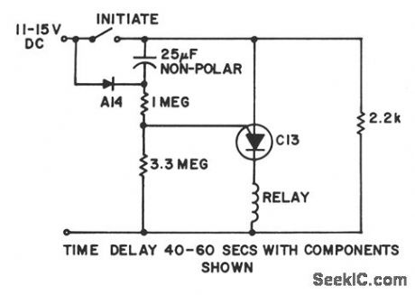
Power is applied to the circuit with the initiate switch open. The 25-μF capacitor charges through the A14, or equivalent, diode and 2.2-KΩ resistor to full supply voltage. When the initiate switch is closed, the low side of the capacitor is suddenly raised to + 12 V. This raises the diode side of the capacitor to approximately +24 V. The capacitor immediately begins discharging through the seriesconnected 1 and 3.3-MΩ resistors. Eventually, the C13 gate becomes forward biased, the device tums, and it applies power to the relay. The delay is virtually independent of supply voltage. (View)
View full Circuit Diagram | Comments | Reading(631)
_ELECTRONIC_TIME_DELAY
Published:2009/7/8 2:18:00 Author:May
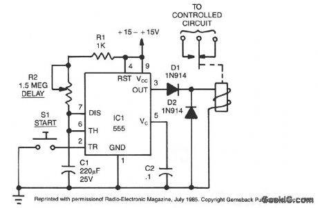
The time delay, T', in seconds is: T = 1.1 x C1 x (R1 + R2). The resistances are in megohms and capacitances in microfarads. The sum of R1 and R2 should not be less than 1000 Ω nor higher than 20 MΩ. Pressing S1 starts the timing cycle. A low-going pulse, instead of S1 can also be used to initiate the timing cycle. With the values shown and allowing for the tolerances of the 200-μF capacitor, the delay will range from 4 minutes and 50 seconds to 7 minutes and 26 seconds. The output terminal, pin 3, of 555, is normally low and switches high during the timing cycle. The output can either sink or source currents up to 200 mA. Therefore, a load such as a relay coil can be connected between pin 3 and VCC or between pin 3 and ground, depending on circuit requirements. When the relay is connected between pin 3 and ground, it is normally de-energized so it is energized only during the timing cycle. Connecting the relay to ground will save power and allow the IC to run cool. (View)
View full Circuit Diagram | Comments | Reading(709)
18_19_MHz_VFO
Published:2009/7/8 2:15:00 Author:May
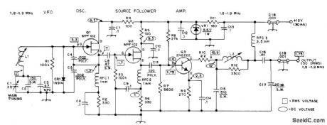

Series-tuned Clapp oscilla-torusing high-impedance JFET at has good fre-quency stability. Diode stabilizes bias. Air variable C1 provides frequency spread of exactly 100 kHz. L1 is 25-58 μH slug-tuned (Miller 43A475CBI). L2 is 10-18.7 μH slug-tuned (Miller 23A155RPC).—D. DeMaw, More Basics on Solid-State Transmitter Design, OST, Nov.1974, p 22-26 and 34. (View)
View full Circuit Diagram | Comments | Reading(1213)
PULSE_AMPLITUDE_DISCRIMINATOR
Published:2009/7/8 2:15:00 Author:May
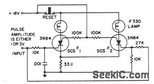
A 1-V amplitude pulse triggers SCS1,but has insufficient amplitude to trigger SCS2.A 3-V mputpulse is delayed h reaching SCS1 by the 10-KΩ and.001-μF integrating network.Instead,it triggers SCS2,then ralses the common emitter voltage to prevent SCS1 from triggering.The 100-KΩ resistors Suppress the rate effect. (View)
View full Circuit Diagram | Comments | Reading(1)
| Pages:965/2234 At 20961962963964965966967968969970971972973974975976977978979980Under 20 |
Circuit Categories
power supply circuit
Amplifier Circuit
Basic Circuit
LED and Light Circuit
Sensor Circuit
Signal Processing
Electrical Equipment Circuit
Control Circuit
Remote Control Circuit
A/D-D/A Converter Circuit
Audio Circuit
Measuring and Test Circuit
Communication Circuit
Computer-Related Circuit
555 Circuit
Automotive Circuit
Repairing Circuit