
Circuit Diagram
Index 973
SSB_EXCITER
Published:2009/7/21 7:23:00 Author:Jessie
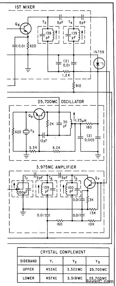
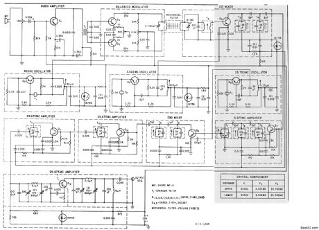
Silicon transistors reduce noise and increase reliability of single-side band exciters. Circuit shown, for 10-meter band, gives choice of upper or lower sideband.-D. L. Wilcox, Single-Sideband Exciter uses Planar Silicon Transistors, Electronics, 35:32, p 65-67. (View)
View full Circuit Diagram | Comments | Reading(1247)
DUTY_CYCLE_MONITOR
Published:2009/7/7 22:29:00 Author:May
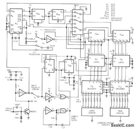
The circuit monitors and displays a digital signal's duty cycle and provides accuracy as high as ±1%.Using switch S2, you can choose a frequency range of either 250 Hz to 2.5 kHz at ±1% accuracy or 2 kHz to 50 kHz at ±10% accuracy. The common-cathode display gives the signal's duty-cycle percentage.Phase-locked loop IC4 and counters IC5A and IC5B multiply the input frequency by a factor of either 10 or 100, depending on switch S2's setting. IC6A and IC6B count this multiplied frequency during the incoming signal's mark interval. IC7 and IC8 then latch this count and display it at the clock's sample rate. For example, if you select a 1% resolution, when the signal's mark period is 40% of the total period, the circuit will enable the counter comprising IC6A and IC6B for 40 counts. To obtain space-interval sampling, you can reverse the input polarity using switch 51. IC2A samples the input signal's period and enables gate IC2C and resets the counter. IC2E and IC2F form the sample-rate clock; IC3B synchronizes the clock's output with the input, so that the circuit can update latches IC7 and IC8.
(View)
View full Circuit Diagram | Comments | Reading(1906)
LOW_POWER_VFO_C_W_80_METER_TRANSMITTER
Published:2009/7/21 7:21:00 Author:Jessie
Power output is 100 mw in amateur band.- Transistor Manual, Seventh Edition, General Electric Co., 1964, p 386. (View)
View full Circuit Diagram | Comments | Reading(826)
SIX_GAME_CHIP_
Published:2009/7/7 22:27:00 Author:May

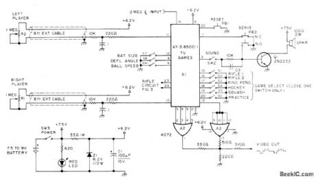
General Instruments AY-3-8500-1 TV game chip and associated circuits give choice of six different games. Article gives additional circuits required, including that for 2MHz master dock whose output is divided in chip to get vertical and horizontal syncfrequencies, VHF modulator used between game and antenna terminal of TV set, and rifle target practice clrcuit,All operate from battery suρply atlower left Article covers construction only ingeneral terms,-s,Ciarcia,Hey,Look What My Daddy Built!,73 Magazine.Oct, 1976,p 104-108 (View)
View full Circuit Diagram | Comments | Reading(2640)
LINE_ACTIVATED_SOLID_STATE_SWITCH
Published:2009/7/7 22:27:00 Author:May
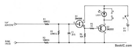
Each and every time a phone on the same line or calling number is taken off-hook, the circuit will be activated to control an extemal electronic circuit. If several extension telephones are used.on one phone line, the circuit can be useful as a busy indicator. LED1 contains a special flashing red LED that makes an excellent indicator for a busy circuit condition.The solid-state switch can be used for several other phone-activated applications, such as automatically tuming on a cassette recorder, starting a phone-use timer or counter, etc. A small relay can be connected at points A and B, in place of LED1, to control extemal circuits. A 117-Vac-to-6-Vdc plug-in power supply can be substituted for the battery to keep the operating cost at a minimum.The 48-Vdc, on-hook, phone-line voltage keeps Q1 in the cut-off condition, allowing no current to flow through resistor R4, hence Q2 remains off. Resistors R1 and R2 keep the solid-state switch circuit from causing any problems with the telephone's central-office equipment. When a phone is taken off-hook, the line voltage (tip to ring) drops to 10 V or less, which forces Q1 to turn on; this, in turn, causes Q2 to trigger LED1, or a relay which might be used in lieu of LED1. (View)
View full Circuit Diagram | Comments | Reading(1262)
LOW_POWER_BROADCAST_BAND_TRANSMITTER
Published:2009/7/21 7:20:00 Author:Jessie
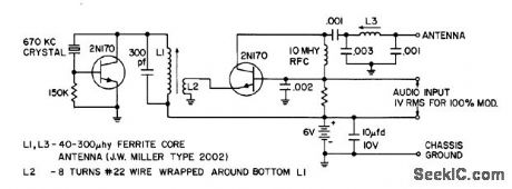
Crystal-controlled 670-kc oscillator and single-transistor amplifier stage provide 400 microwatts a-m for antenna.- Transistor Manual, Seventh Edition, General Electric Co., 1964, p 386. (View)
View full Circuit Diagram | Comments | Reading(909)
SUBTRACTOR
Published:2009/7/7 22:26:00 Author:May
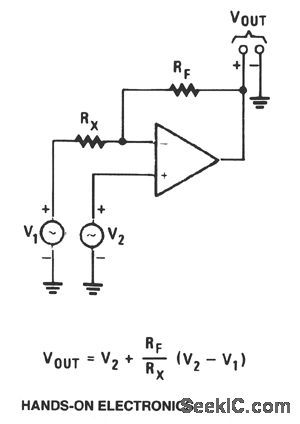
View full Circuit Diagram | Comments | Reading(721)
_ADDER
Published:2009/7/7 22:26:00 Author:May

View full Circuit Diagram | Comments | Reading(578)
DIVIDE_MULTIPLY_WITH_ONLY_ONE_TRIM
Published:2009/7/7 22:25:00 Author:May
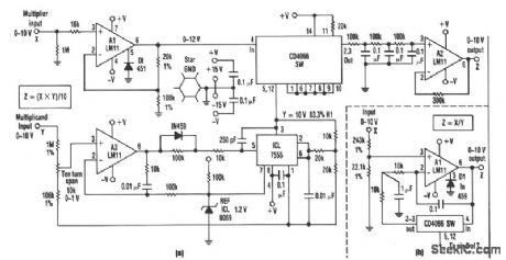
This relatively simple, inexpensive circuit requiring one trimming operation can multiply or divide with a consistent accuracy of greater than 1 part in 1,000. An inexpensive CMOS version of standard 555 timer chip T, in conjunction with low-drift LM11 error amplifier A3, an inexpensive analog chopper switch SW, form a unique voltage-to-duty-cycle converter to produce the difficult transfer function necessary for accurate conversion.An unknown multiplicand voltage applied to the A3 error op amp circuit's Y input controls the duty cycle of the timer through its pin 5 modulation input. The network between the sink-and-source output of the timer, pin 3, and the state trigger inputs, pins 2 and 6, cause the timer to oscillate. An error feedback signal from the timer's discharge output, pin 7, represents the duty cycle. Integrating this duty-cycle signal with voltage reference REF representing full scale, and applying the result to the inverting input of A3, closes the feedback loop and insures high accuracy.Multiplier X feeds into another LM11 op amp, A1, which acts as a input buffer and scaler. A third LM11, A2 filters and buffers the Z output. Between A1 and A2, the timer's duty-cycle output modulates the analog switches of a CD4066 to achieve the desired multiplier output. To perform division instead of multiplication, reconfigure the op amp AI circuit with the use of jumpers. Amplifier A2 isn't required in the division configuration.To calibrate the circuit, connect the X and Y inputs together and apply 10 V. Then adjust the 10-turn span potentiometer to achieve a 10-V output at Z for multiplication, or 1 V for the division configuration.Also check for zero output at a zero multiplier input. The circuit is scaled for 0-10 V inputs and outputs with a small overtage capability, but other scalings are possible. Star grounding or a heavy ground bus should be used to reduce offset problems that are unavoidable in this design. (View)
View full Circuit Diagram | Comments | Reading(1075)
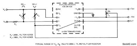
ROOT_SUM_SQUARED
Published:2009/7/7 22:24:00 Author:May
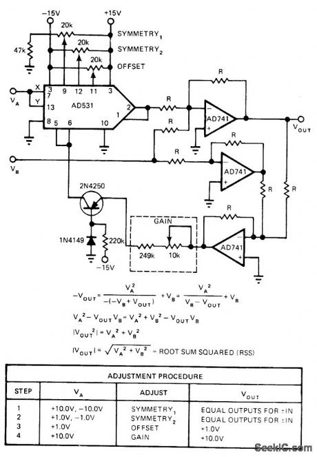
Vector summation circuit uses AD531 variable-gain analog multiplier. Starting with trimpots centered and input VB grounded, apply specified DC voltages to input VA and adjust trimpots for output specified in table.-R. Frantz, Analog Multipliers-New IC Versions Manipulate Real-World Phenomena with Ease, EDN Magazine, Sept. 5, 1977, p 125-129. (View)
View full Circuit Diagram | Comments | Reading(748)
ColorTV_358_MHz_crystal_oscillator_using_a_dual_gate_MOSFET
Published:2009/7/21 7:19:00 Author:Jessie
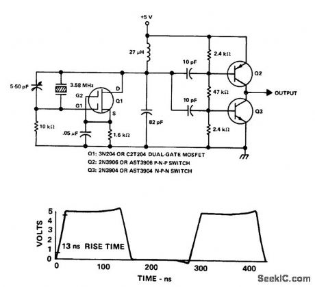
ColorTV 3.58 MHz crystal oscillator using a dual-gate MOSFET (courtesy Texas Instruments Incorporated). (View)
View full Circuit Diagram | Comments | Reading(1490)
_LVDT_DRIVER_DEMODULATOR
Published:2009/7/7 22:21:00 Author:May
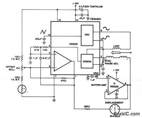
A very simple motion transducer can be constructed using the circuit shown. The output is biased to one-half the supply voltage. This requires special interface circuitry for the signal readout. One simple method is to use a zero center meter in a bridge configuration. Displacement now can be measured as a positive or negative meter reading. Readout sensitivity is a function of the particular LVDT and of the gain of the error amplifier. Dc offsets can be nulled by using a simple offset adjustment circuit as indicated. (View)
View full Circuit Diagram | Comments | Reading(1283)
LINEARIZING_MODULAR_MULTIPLIER
Published:2009/7/7 22:21:00 Author:May


Adding three external resistors to conventional transconductance multiplier reduces fedthrough,decreases average nonlinearity,and cuts ouerall error in half.Article gives adjustment procedure,-L.Counts,Reduce Multiplier Errors by to an Order of Magnitude,EDN Magazine,March20,1974,p65-68 (View)
View full Circuit Diagram | Comments | Reading(651)
Color_TV_automatic_resolution_control
Published:2009/7/21 7:17:00 Author:Jessie
Color TV automatic resolution control (courtesy GTE Sylvania Incorporated). (View)
View full Circuit Diagram | Comments | Reading(751)
PHONE_RECORDER
Published:2009/7/7 22:21:00 Author:May
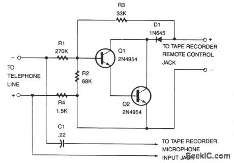
This recorder can be connected to the telephone lines just about any place, and no external power source is needed. The tape recorder's switch terminals are applied to a pair of transistors, connected as Darlingtons, that are used to turn the recorder on and off. When the telephone is off-hook there's usually about 50 Vdc across the phone that's divided over R1, R2, and R4, so that Q1's base is negative enough to keep the recorder off. Pick up the receiver, and the voltage drops to 5 V. That leaves not quite-enough voltage on Q1's base to keep that transistor at cutoff, so the recorder begins. Remember to keep your recorder's switch in the on position, and depending on how many people use the telephone, remember to rewind or change tapes occasionally! (View)
View full Circuit Diagram | Comments | Reading(1217)
OUTPUT_LIMITER
Published:2009/7/7 22:21:00 Author:May
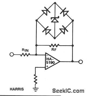
HA-5190 is rated for ±5 V output swing, and saturates at ±7 V. As with most op amps, recovery from output saturation is slow compared to the amplifier's normal response time. Some form of limiting, either of the input signal or in the feedback path, is desirable if saturation might occur. The circuit illustrates a feedback limiter, where gain is reduced if the output exceeds ± ( Vz + 2 Vf). A 5-V zener with a sharp knee characteristic is recommended. (View)
View full Circuit Diagram | Comments | Reading(880)
DYNAMIC_NOISE_REDUCTION_CIRCUIT
Published:2009/7/7 22:19:00 Author:May
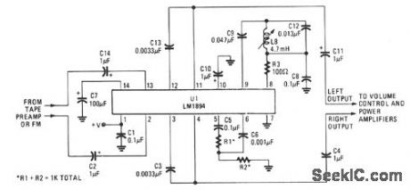
View full Circuit Diagram | Comments | Reading(690)
NOISE_LIMITER
Published:2009/7/7 22:19:00 Author:May
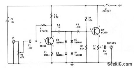
This circuit is fed from the earphone jack of your receiver and goes to limiter control R6 and is then amplified by Q1: a common-emitter stage that has a voltage gain of only about 10, because of the negative feedback introduced by R3. The output of Q1 is fed to a simple clipping circuit, consisting of diodes Dl through D4. The diodes, connected in pairs, act like Zeners with an avalanche rating of about 1 V. The two pairs are connected opposite in polarity to each other, so that the audio signal is clipped at about 1 V. The signal is then coupled to the output socket through an emitter-follower buffer stage built around Q2 and an output attenuator control R7. (View)
View full Circuit Diagram | Comments | Reading(995)
1_W_AT_50_MC
Published:2009/7/21 7:34:00 Author:Jessie
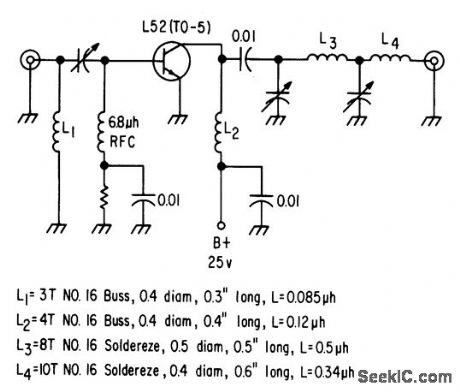
Relatively high breakdown voltage of L52 transistor permits amplitude modulation. Overall efficiency is 65%. Combination pi-L network matches common emitter class-C stage to 50-ohm antenna.-Texas Instruments Inc., Solid-State Communications, McGraw-Hill, N.Y., 1966, p 322. (View)
View full Circuit Diagram | Comments | Reading(665)
F_M_WIRELESS_MIKE
Published:2009/7/21 7:33:00 Author:Jessie
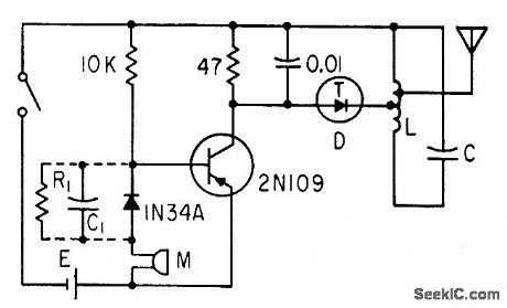
Oscillator. modulator using single tunnel diode produces 35-kc frequency deviation per my of modulating signal at 90 Mc. When fed by dynamic mike, range is up to 100 feet. If pre-emphasis is desired, diode 1N34A may be replaced by R1-C1 circuit shown in dotted lines, having time constant of 75 microsec.-W. Ko, Tunnel Diode F.M Wireless Microphone, Electronics, 33:47, p 93-95. (View)
View full Circuit Diagram | Comments | Reading(2215)
| Pages:973/2234 At 20961962963964965966967968969970971972973974975976977978979980Under 20 |
Circuit Categories
power supply circuit
Amplifier Circuit
Basic Circuit
LED and Light Circuit
Sensor Circuit
Signal Processing
Electrical Equipment Circuit
Control Circuit
Remote Control Circuit
A/D-D/A Converter Circuit
Audio Circuit
Measuring and Test Circuit
Communication Circuit
Computer-Related Circuit
555 Circuit
Automotive Circuit
Repairing Circuit