
Circuit Diagram
Index 966
CLOSED_LOOP_TRACER
Published:2009/7/8 2:13:00 Author:May
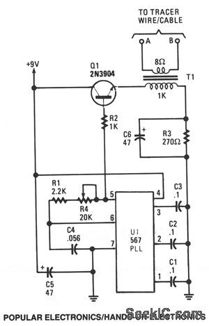
The tracer, consisting of both a transmitter and receiver, is designed to follow a closed-loop wire or cable system. It follows an induced voltage path created by feeding a low-current, audio-frequency signal through the cable. When the pick-up coils come within close proximity of the current-carrying cable, a small voltage is generated in each coil, and that induced voltage is then processed by the receiver's circuitry.
The circuit is built around a 567 phase-locked loop (PLL) configured as a variable-frequency, audio-generator circuit, which is designed to produce a square-wave output at pin 5. Potentiometer R4 allows the oscillator to be easily tuned to the receiver's frequency. Transistor Q1 isolates the oscillator from the load and matches the impedance of the primary of T1. Resistor R3 limits current flow through Q1. The low-impedance secondary of T1 supplies the cable drive signal. (View)
View full Circuit Diagram | Comments | Reading(3497)
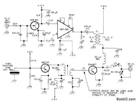
20_MHz_PHONE
Published:2009/7/8 2:13:00 Author:May
Colpitts oscillator using HEP 53 provides excellent stability with third-over-tone crystal. Power amplifier stage uses 2N4427 in class C common-emitter stage modulated through collector circuit, to develop about 1.25-W output at 28 MHz. HEP 801 FET microphone amplifier provides high-impedance input for crystal microphone and drives HEP 593 IC to give about 1-W AF output. Article covers con-struction and tune-up.-B. Johnston, Little Bill, 73Magazine, July 1974, p 63-64 and 66-67. (View)
View full Circuit Diagram | Comments | Reading(1592)
DOWNBEAT_EMPHASIZED_ELECTRONIC_METRONOME
Published:2009/7/8 2:12:00 Author:May
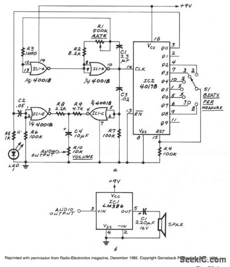
IC1a and IC1b form an astable multivibrator. The astable's signal is fed to IC1c, also to the clock input of IC2, a 4017B decade counter. That IC's Q0 through Q9 outputs become high one at a time for each successive clock pulse received at pin 14. Switch S1 feeds one of those outputs to the 4017B's reset input. Whenever the selected output becomes high, the 4017B restarts its counting cycle; that determines the number of beats per measure. The network composed of C2 and R6 sharpens the downbeat pulse, and the network composed of C3 and R7 sharpens the free-running pulses. By making C2 larger than C3, the downbeat receives greater emphasis.
(View)
View full Circuit Diagram | Comments | Reading(644)
DIGITIZER
Published:2009/7/8 2:12:00 Author:May
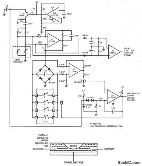
If the tube is level with respect to gravity, the bubble resides in the tube's center and the electrode resistances to common are identical. As the tube shifts avqr from level, the resistances increase and decrease proportionally. Transducers of this type must be excited with an ac waveform to avoid damage to the partially conductive liquid inside the tube.
The level transducer is configured with a pair of 2-KΩ resistors to form a bridge. The required ac bridge excitation is developed at C1A, configured as a multivibrator. C1 biases Q1, which switches the LT1009's 2.5-V potential through the 100-μF capacitor to provide the ac bridge drive. The bridge differential output ac signal is converted to a current by A1, operating as a Howland current pump. This current, whose polarity reverses as bridge drive polarity switches, is rectified by the diode bridge. Thus, the 0.03-μF capacitor receives unipolar charge. A2, running at a differential gain of 2, senses the voltage across the capacitor and presents its single-ended output to C1B. When the voltage across the 0.03-μF capacitor becomes high enough, C1B's output becomes high, turning on the paralleled sections of the LTC1043 switch. This discharges the capacitor. The 47-pF capacitor provides enough ac feedback around CIB to allow a complete zero reset for the capacitor. When the ac feedback ceases, C1B's output decreases and the LTC1043 switch goes off. The 0.03-μF unit again receives constant current charging and the entire cycle repeats. The frequency of this oscillation is determined by the magnitude of the constant current delivered to the bridge-capacitor configuration. This current's magnitude is determined by the transducer bridge's offset, which is level related. (View)
View full Circuit Diagram | Comments | Reading(1154)
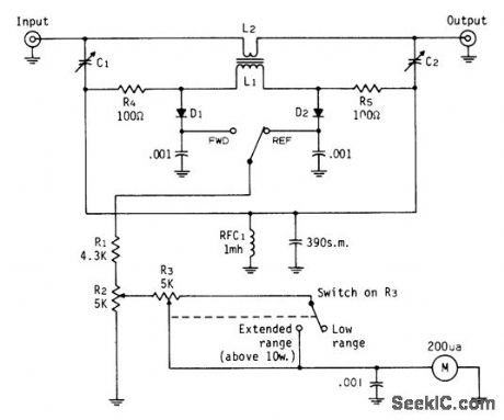
RF_WATTM_ETER
Published:2009/7/8 2:11:00 Author:May
Calibration is accurate on all HF bands because circuit is not frequency-sen-sitive. Sensitivity depends on metermovement, number of turns in primary coil, and resistive voltage divider. With values shown, pots can be adjusted for full-scale values from 1-14 W. C1 and C2 are 3-20 pF. Diodes are 1N34A, 1N60, or equivalent. L1 is 46 turns No. 28 on Amidon T-50-2 toroid, with 2 turns No. 22 between ends of L1 for L2. To adjust, connect resistive dummy load to one coax receptacle and RF power source to other, with R2 at maximum resistance.Place upper switch in position providing high-est meter reading, and make that the FWD position. Switch to other position, which becomes REF, and adjust C1 for null reading. Reverse RF source and load, leaving switch at FWD, and ad-iust C2 for null. Wattmeter can now be cali-brated.—A. Weiss, ORP Low-Low Power Opert ating, CQ Jan. 1974, p 42-44 and 80. (View)
View full Circuit Diagram | Comments | Reading(1869)
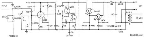
CONSTANT_CURRENT_STIMULATOR
Published:2009/7/8 2:10:00 Author:May
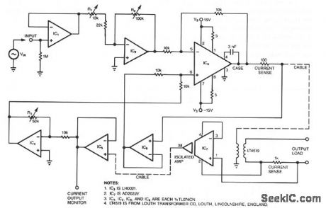

Most circuits that provide an electrical stimulus for research subjects are constant-voltage designs; this circuit is a constant-current design. Stimulator circuits must be isolated for two reasons: to ensure safety and to minimize interference. Isolated stimulators are essentially two-terminal devices; output currents can flow only between the two output terminals and can at no time flow through any other path, such as the power ground.
The circuit's bandwidth ranges from 50 Hz to 5 kHz when a ± 1 V sinusoidal input drives the circuit.Output loads can range from a short circuit to 100 KΩ and have as much as 0.033 μF of parallel capacitance. The transformer and associated circuitry conveniently connect to the main circuit via a cable. Note: This circuit is not approved for use on human beings.
Op amps, IC1 and IC2, buffer and set the gain of the circuit, respectively. You adjust trimmer R1 so that R2, a 10-turn pot, yields output currents ranging from 0 to 1 mA/VIN. IC3 is a power op amp. Its output drives the primary of a transformer that has a current gain of 0.1, or avoltage gain of10. Operating from a + 15 V supply, the transformer therefore has a voltage compliance of ±150 V.
The circuit senses not only the current supplied to the transformer but also the current in the transformer's secondary. IC7, a fully isolated, medical-grade amplifier, provides the isolated feedback signal because the op amp has its own built-in isolation transformer. Trimmer R3 sets the feedback gain precisely at 27 KΩ nominal. (View)
View full Circuit Diagram | Comments | Reading(1388)
STIMULUS_ISOLATOR
Published:2009/7/8 2:09:00 Author:May
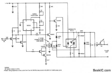
This stimulus isolator uses a photo-SCR and a toroid for shaping pulses of up to 200 V at 200μA.
(View)
View full Circuit Diagram | Comments | Reading(625)
BREATH_MONITOR
Published:2009/7/8 2:07:00 Author:May
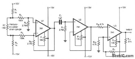
The mercury-in-rubber strain gauge is the detector of breathing. In the model device, the strain gauge produced by Meclimatic, Demark was used. The change in the length of the strain gauge wrapped around the chest during breathing causes a varying electrical resistance of about 0.2 Ω/cm. The constant current passing R1, RT and R4 gives the constant component on the output of U1 differential amplifier. The change in the resistance of the strain gauge, which results from breathing, produces proportional varying in output voltage of U1 amplifier. The voltage follower, based on U2, separates the output voltage of the filter from the input stage amplifier. U3 works as a noninverter amplifier with regulated gain. This device should be supplied with a stabilized constant voltage of ±15 V. (View)
View full Circuit Diagram | Comments | Reading(1771)
Color_TV_chroma_signal_processor
Published:2009/7/21 6:21:00 Author:Jessie
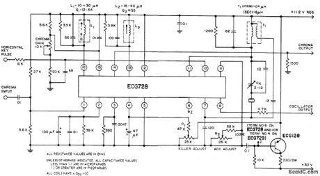
Color TV chroma signal processor. The ECG728 provides subcarrier regeneration and total chroma signal processing prior to demodulation. The coils of the chroma amplifier and bandpass amplifier are stagger-tuned to provide a com-bined typical bandpass of 3.08 to 4.08 MHz. A burst separator amplifier injects the burst signal into the 3.58 MHz oscillator. The ACC detector and killer detector sense the burst level or absence of burst, respectively, by monitoring the osoil-lator's response to the burst injection level. The thresholdsfor the ACC and killer are independently adjusted by resistors R2 and R1 at terminals 9 and 4. The chroma input is at pin 14 and the oscillator output is at pin 8.Pin 6 is a zener diode for use as a regulated voltage reference at 11.9 volts (courtesy GTE Sylvania Incorporated). (View)
View full Circuit Diagram | Comments | Reading(903)
LOW_NOISE_FET_PREAMPLIFIER
Published:2009/7/21 6:21:00 Author:Jessie
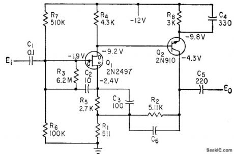
For 600-ohm source, 3-db response is 0.5 cps to 700 kc, with voltage gain of 10.5, using common-emitter direct-coupled amplifier stage after fet stage, with 26 db of feedback. With 1-meg source, upper limit is 20 kc.-E. G. Fleenor, Low-Noise Preamplifier Uses Field-Effect Transistors, Electronics, 36:15, p 67-69. (View)
View full Circuit Diagram | Comments | Reading(1654)
10_CPS_TO_100_KG_BANDPASS
Published:2009/7/21 6:20:00 Author:Jessie
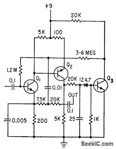
Input impedance is over 1 meg. Can be used in microphone case to raise power level of signal above that of interference. Both positive and negative feedback are used. Q1 and Q3 are 2N1086A, and Q2 is 2N414.-J. J. Tiemann, Transistor Amplifier with Adjustable Impedance and Gain, Electronics, 35:15, p 68-69. (View)
View full Circuit Diagram | Comments | Reading(764)
AUTOMATIC_INPUT_IMPEDANCE_MATCHER
Published:2009/7/21 6:18:00 Author:Jessie
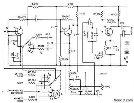
Uses controlled amounts of negative feedback to maintain practically constant voltage sensitivity for impedances from 10 ohms to over 10,000 ohms.-Preamp Matches Input Impedance, Electronics, 31:13, p 81. (View)
View full Circuit Diagram | Comments | Reading(680)
30_MC_VARIABLE_BANDWIDTH_RADAR_PREAMP
Published:2009/7/21 6:17:00 Author:Jessie
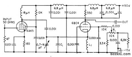
Bias control R1 on grounded-grid 6BC4 triode provides continuous change of bandwidth from 200 kc to 15 Mc, for changing search range. Insertion loss is 0 db.-R. Hirsch, Voltage-Variable Bandwidth Filter, Electronics, 35:22, p 46-47. (View)
View full Circuit Diagram | Comments | Reading(966)
Triac_heater_temperature_control_circuit
Published:2009/7/21 6:16:00 Author:Jessie
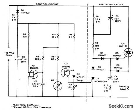
Triac heater temperature control circuit (courtesy Motorola Semiconductor Products Inc.). (View)
View full Circuit Diagram | Comments | Reading(2202)
Color_TV_chroma_processing_system_with_a_PLL_featuring_APC_and_ACC
Published:2009/7/21 6:15:00 Author:Jessie
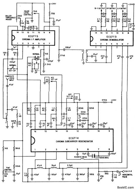
Color TV chroma processing system with a PLL featuring APC and ACC (courtesy GTE Sylvania Incorporated). (View)
View full Circuit Diagram | Comments | Reading(830)
L_F_D_F_PREAMP
Published:2009/7/21 6:15:00 Author:Jessie
Negative feedback provides stability, yet gain is sufficient so noise contributions of preamplifier to 15-500 kc direction-finding receiver are negligible. Output of preamp feeds receiver through 100 feet of 100-ohm balanced transmission line.-L. E. Orsak and D. W. Martin, Direction Finding at Low Frequencies, Electronics, 33:38, p 74-77. (View)
View full Circuit Diagram | Comments | Reading(622)
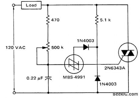
Low_cost_light_dimmer_using_an_SBS_and_triac
Published:2009/7/21 6:14:00 Author:Jessie

Low-cost light dimmer using an SBS and triac. Shunting the SBS with two 20K resistors minimizes the flash-on effect (courtesy Motorola Semiconductor Products Inc.). (View)
View full Circuit Diagram | Comments | Reading(967)
ELECTROMETER_PREAMP
Published:2009/7/21 6:13:00 Author:Jessie
Transformer T1 feeds drive coil of vibrating capacitor C1 used in place of conventional chopper for measuring picoampere currents. Output of electrometer, taken from Q2 of preamp, goes to amplifier that is source of feedback signal. -V. J. Caldecourt, Using a Vibrating Capacitor as an Electrometer Input, Electronics, 35:14, p 48-50. (View)
View full Circuit Diagram | Comments | Reading(1352)
Triac_overvoltage_protection_circuit_with_automatic_reset
Published:2009/7/21 6:13:00 Author:Jessie
Triac overvoltage protection circuit with automatic reset. If the voltage at point A exceeds 11 volts during any half-cycle D6 fires and turns on SOB Q1, removing power from the load (courtesy Motorola Semiconductor Products Inc.). (View)
View full Circuit Diagram | Comments | Reading(1473)
Hysteresis_free_power_controller_using_an_SBS_and_a_triac
Published:2009/7/21 6:10:00 Author:Jessie
Hysteresis-free power controller using an SBS and a triac (courtesy Motorola Semiconductor Products Inc.). (View)
View full Circuit Diagram | Comments | Reading(806)
| Pages:966/2234 At 20961962963964965966967968969970971972973974975976977978979980Under 20 |
Circuit Categories
power supply circuit
Amplifier Circuit
Basic Circuit
LED and Light Circuit
Sensor Circuit
Signal Processing
Electrical Equipment Circuit
Control Circuit
Remote Control Circuit
A/D-D/A Converter Circuit
Audio Circuit
Measuring and Test Circuit
Communication Circuit
Computer-Related Circuit
555 Circuit
Automotive Circuit
Repairing Circuit