
Circuit Diagram
Index 977
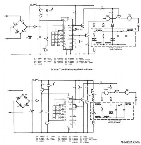
TONE_DIALING_TELEPHONE
Published:2009/7/7 21:11:00 Author:May
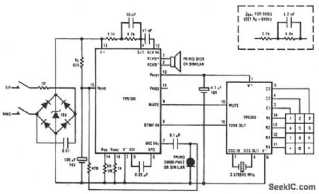
This circuit shows the TP5700 directly interfacing to a low-voltage DTMF generator.VREG1 supplies the necessary 2-V minimum bias to enable the TP5380 to sense key closures and pull its mute output high.VREG1 then switches to a 3-V regulated output to sustain the tone dialer during tone generation. The TP5700 DTMF input incorporates the necessary load resistor to V- and provides gain, plus AGC action, to compensate for loop length. A muted tone level is heard in the receiver. For DTMF generators with a higher output level than the TP5380, a resistive potentiometer should be added to reduce the level at the speech circuit DTMF input. (View)
View full Circuit Diagram | Comments | Reading(4643)
WATER_LEAK_ISOLATOR
Published:2009/7/7 21:10:00 Author:May
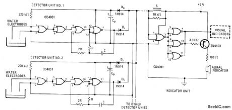
Master indicator monitors large number of two-electrode waterleak detectors simultaneously, with each detector indicating presence of water by producing unique tone signal. Only two wires are needed between detectors and master indicator unit.Each detector location has quad NOR gate. First gate is water sensor, second is inverter, and last two form astable MVBR. When sensing electrodes are dry, resistance between them is above 500K and MVBR is disabled. When water drops resistance below 100K, MVBR oscillates at audio frequency determined by its RC time constant, equal to 1/1.4RC where R is in ohms and C is in farads. CP value in farads should be 1/1000 of lowest frequency used by detectors. L in henrys is about 1/600 of lowest frequency.-F. E. Hinkle, Multiplexed Detectors lsolate Water Leaks, Electronics, Dec. 11, 197S, p 116-117. (View)
View full Circuit Diagram | Comments | Reading(2635)
VISIBLE_RED_CONTINUOUS_LASER_GUN
Published:2009/7/7 21:09:00 Author:May


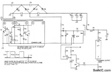
Q1 and Q2 switch the primary windings of transformer T1 via a square wave at a frequency determined by its magnetic properties. Diodes Dl and D2 provide base return paths for the feedback current of Q1 and Q2. The output winding of T1 is connected to a multiple section voltage multiplier. That multiplier consists of capacitors C1 through C5 and diodes D3 through D6. Resistors R3 and R4 divide the 800 V taken off at the junction of C3, and C5 for charging the dump capacitor C9 in the ignitor circuit. The ignitor, consisting of the T2 pulse transformer and capacitor discharge circuitry, provides the high-voltage dc pulse to ignite the laser the SCR1 dumping the energy of capacitor C9 into the primary of T2. The high-voltage pulses in capacitor C11 through rectifier diode D9. When C11 is charged to a LT1, ignition takes place and a current now flows that is sufficient to sustain itself at the lower voltage output of the voltage multiplier section. The path for this sustaining current is through the secondary of T2 and ballast resistors R11 and R12. The ignitor circuit is now deactivated by the clamping of Q3 emitter via Q4 being turned on by the voltage drop occurring across R10. This voltage drop will only occur when the laser tube is ignited and causes the SCR1 to cease firing; otherwise, the ignitor circuit would continue to operate, unnecessarily drawing on the limited power available.
(View)
View full Circuit Diagram | Comments | Reading(782)
RINGER_RELAY
Published:2009/7/7 21:06:00 Author:May
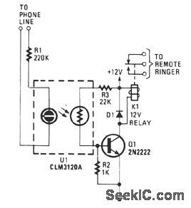
When the phone rings, the ring signal from the telephone company lights a neon lamp within a CLM3120 optocoupler. That causes a drop in the resistance of the CdS cell output of the device, turning on transistor Q1. When Q1 tums on, relay K1 is energized. The circuit should be connected in series with the lamp that is to be activated. (View)
View full Circuit Diagram | Comments | Reading(995)
SIX_GAME_VIDEO
Published:2009/7/7 21:05:00 Author:May

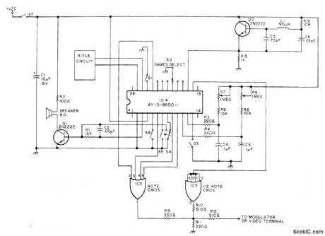
General Instruments AY-3-8500-1 MOS chip gives choice of hockey, squash, tennis, two types of rifle shoot, and practice games, all with sound effects and automatic scoring on 0-15 display at top of TV screen.Can be used with standard TV receiver (using RF modulator circuit) or with video monitor, S4 grounds base of Q1 when in manualserve mode, to eliminate steady boing when ball leaves playing field. R5-R8 position players on field.Article covers operation in detail and gives suitable rifle circuit. Supply is +6V. 2-MHz clock is at upper right.-A. Dorman, Six Games on a Chip, Kilobaud,Jan. 1977, p 130, 132, 134, 136, and 138. (View)
View full Circuit Diagram | Comments | Reading(3466)
FOUR_CHANNEL_ANALOG_MULTIPLEXER
Published:2009/7/7 21:04:00 Author:May

Buffered input and output provide very high input impedance and low output impedance for analog signal selection or time-division multiplexing with Harris HA-2400/HA-2405 IC that combines functions of analog switch and high-performance opamp. Bandwidth is about 8 MHz. Signal is fed back from output to digitally selected input channel to place that channel in voltage-follower configuration with noninverting unity gain.- Linear & Data Acquisition Products, Harris Semiconductor, Melbourne, FL, Vol. 1, 1977, p 7-36-7-38 (Application Note 514). (View)
View full Circuit Diagram | Comments | Reading(2830)
ELECTRONIC_TELEPHONE_SET_WITH_REDIAL
Published:2009/7/7 21:03:00 Author:May
View full Circuit Diagram | Comments | Reading(996)
TWO_CHANNE_LOGIC_CONTROLLED
Published:2009/7/7 21:02:00 Author:May
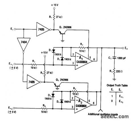
Two CA3080A operational transconductance amplifiers are programmed on and off alternately by control logic, for multiplexing two inputs each up to ±5 V into single output. When control line E, is high or 1, input 1 appears at output; for logic 0, input 2 appears at output. Both channels operate at unity gain. Control logic is TTL-compatible.-W. G. Jung, IC Op-Amp Cookbook, Howard W. Sams, Indianapolis, IN, 1974, p 458-462. (View)
View full Circuit Diagram | Comments | Reading(734)
EIGHT_CHANNEL_MUX_DEMUX
Published:2009/7/7 20:58:00 Author:May

Provides for monitoring of all eight channels continuously at remote location instead of scanning channels at receiver, Each output of DG508 eight-channel analog multiplexor in receiver feeds its own opamp for driving readout. Similar DG508 at transmitter feeds inputs over single-wire line under control of MM74C90 presettable decade counter which also feeds pulse train over separate channel to receiver for timing and synchronization. 15-V reset pulse superimposed on 5-V clock pulses keeps channels synchronized.- Analog Switches and Their Applications, Siliconix, Santa Clara, CA, 1976,p 7-71-7-74. (View)
View full Circuit Diagram | Comments | Reading(1084)
OSCILLATOR_FOR_CHANNELS_2_6
Published:2009/7/7 20:56:00 Author:May
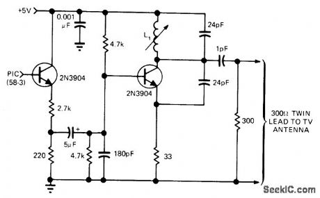
Transmitter serving as interface between video game and TV set can be tuned with L1 to vacant chan, nol in low TV band. Regular antenna should be disconnected when output of oscillator is fed to TV set via twin-line, to avoid broadcasting game signals. L1 is 4tums No. 18 spaced 3/8 inch on 1/4-inch slug-tuned form.-B. Matteson, King Pong Game Offers Hockey and Tennis Alternatives to TV Re-Runs, EDN Magazine, Aug. 5, 1975, p 47-55. (View)
View full Circuit Diagram | Comments | Reading(857)
HANDS_FREE_TELEPHONE
Published:2009/7/7 20:55:00 Author:May
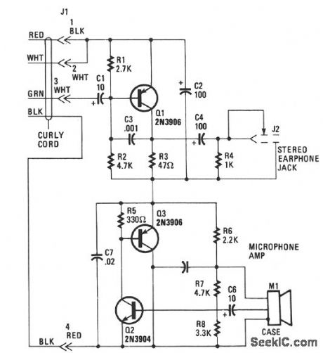
Transistor Q1 of the headset amplifier circuit amplifies the 30 mV signal, that would have gone to the earphones, to.5 V, which sufficiently drives the stereo earphones. Capacitor C1 blocks any dc current from shorting back into the telephone base. Capacitor C2 provides the very important ac signal short around the amplifier. Capacitor C3 provides high-frequency rolloff characteristics and prevents the amplifier from oscillating. Capacitor C4 is a dc block to the 35-Ω impedance of the stereo earphones, and resistor R4 bleeds off any charge build up to prevent a popping sound when the stereo earphones are plugged into the mini-earphone jack J2. The headset amplifier has only about 2 Vdc across it. The microphone amplifier circuit is composed of transistors Q2 and Q3 in an inverted-Darlington configuration.Another, and perhaps easier, way to understand the operation of this circuit is to consider Q3 as an emitter-follower stage. The electret microphone has a built-in FET IC amplifier that needs at least 3 V at 0.4 mA of clean supply power in order to provide an output impedance of 200 to 800 Ω. Resistors R6 and C5 provide that clean dc power to the FET IC and also provide the bias to Q2 without an ac feedback, which would have reduced Q2's gain. Capacitor CG blocks the output dc bias from the FET IC. (View)
View full Circuit Diagram | Comments | Reading(1127)
VHF_MODULATOR_
Published:2009/7/7 20:52:00 Author:May
Developed as interface between General Instruments AY-3-8500-1 TV game chip and antenna terminal of TV set. Adjust C1 to frequency of unused channel to which receiver is set for playing games. Article gives all circuits but covers construction only in general terms.-S. Ciarcia, Hey, Look What My Daddy Built!, 73 Magazine, Oct. 1976, p 104-108. (View)
View full Circuit Diagram | Comments | Reading(3028)
TELEPHONE_CONTROLLED_NIGHT_LIGHT
Published:2009/7/7 20:50:00 Author:May
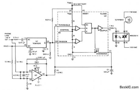
When the telephone rings, or when the handset is lifted, the night light is turned on and remains on while the conversation takes place. When the handset is replaced in the cradle, the light remains on for about 11 s. During standby conditions, the -28 Vdc bias on the phone line maintains the output of U3 in a high state. When the ac ring signal is applied to the phone line, it is processed by the ring detector U1, producing a negative output pulse at pin 2 for each ring. These pulses trigger U2, causing its output to become high and the discharge transistor to turn off. The high output of U2 activates optoisolator U4, which turns on the night light. Each ring retriggers the timer and discharges C1, preventing it from reach-ing the 2/3 VDD threshold level. Thus, the night light will remain on while the phone is ringing and for about 11 s after the last ring. After 11 s, C1 will be charged to the U2 threshold level (2/3 VDD) resulting in the U2 output returning to a low level and its discharge output turning on, discharging C1. The lamp will turn off if the phone is not answered.
When the phone is answered, a 1-KΩ load is placed across the phone. This removes the differential input to op amp U3, causing its output to become low, and capacitor C1 starts discharging through R1. As long as the voltage across C1 remains low, timer U2 cannot start its cycle and the lamp will remain on. When the phone is hung up, the low impedance is removed from the phone line and the differential voltage across the line causes the U3 output to become high. This allows C1 to start charging, initiating the timing that will turn off the night light. (View)
View full Circuit Diagram | Comments | Reading(1163)
60_LED_HYPNOTIC_SPIRAL
Published:2009/7/7 20:50:00 Author:May

LEDs are mounted on display board in spiral arrangement and wired in matrix connected to ICs so each LED is lighted in sequence as IC1 and lC2 carry out counting function. IC3 is square-wave oscillator with frequency determined by C1 and setting of R2. Output pulses are used to clock lC1 to advance count, with carry output of IC1 clocking every tenth count. At end of 60 counts, both ICs reset to zero for new sequence. Inherent current limiting of ICs makes dropping resistors unnecessary for LEDs.-F. Blechman, Digitrance, Modern Electronics, Dec, 1978, p 29-31. (View)
View full Circuit Diagram | Comments | Reading(3660)
16_CHANNEL_SIMPLIFIED_SEQUENTIAL_MUL_TIPLEXING
Published:2009/7/7 20:46:00 Author:May
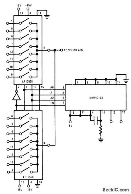
Two National LF13508 eight-channel multiplexors are connected so enable pins are used to disconnect one multiplexer while the other is sampling. Any number of eight-channel multiplexers can be connected in this way if speed is not prime system requirement.- FET Databook, National Semiconductor, Santa Clara, CA, 1977, p 5-79-5-81. (View)
View full Circuit Diagram | Comments | Reading(764)
TV_GAME_CONTROLLER
Published:2009/7/7 20:45:00 Author:May
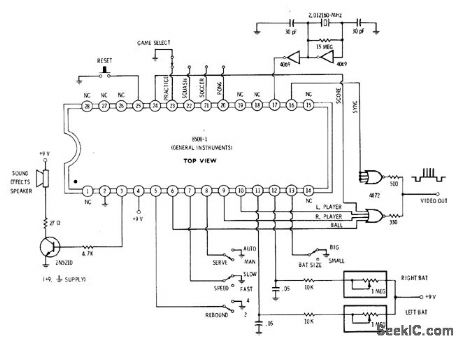
Single General Instruments 8500 lC contains most of electronics needed for pong, hockey, squash, or practice games using screen of TV set. Desired game is selected by grounding one of pins 20-23. Connect ball, player, and score outputs to four-input 0R circuit to generate composite video for com bining with sync output. Final output can be fed directly to video amplifier of TV set or fed to suitable RF modulator. Sound output is fed to Ioudspeaker through transistor audio amplifier.No connection on pin 5 gives two rebound angles, while grounding gives four rebound an gles. Open pin 7 gives fast speed, and grounding gives slow speed. 0pen pin 13 gives small bats, and grounding gives large bats.-D. Lan-caster, CMOS Cookbook, Howard W. Sams, Indianapolis, IN, 1977, p 166. (View)
View full Circuit Diagram | Comments | Reading(1120)
SINGLE_CHIP_PULSE_TONE_DIALER
Published:2009/7/7 20:43:00 Author:May
The XR-75990 single-chip pulse/tone Dialer is a silicon gate CMOS circuit which performs both pulse and tone functions. It is designed to operate directly from the telephone line or on a separate small power supply. A 17-digit buffer is provided for redial feature. (View)
View full Circuit Diagram | Comments | Reading(2116)
HIGH_SPEED_16_CHANNEL
Published:2009/7/7 20:43:00 Author:May
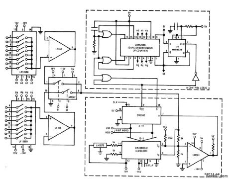
Fast two-channel multiplexer using National AM182 dual analog switch provides second-level multiplexing by accepting outputs of each LF13508 eight-channel multiplexer and feeding these outputs sequentially into 8-bit successive-approximation A/D converter. Technique makes throughput rate of system independent of analog switch speed. With maximum clock frequency of 4.5MHz,throughput rate is 31.250 samples per second per channel- FET Databook, National Semiconductor, Santa Clara, CA, 1977, p 5-79-5-80. (View)
View full Circuit Diagram | Comments | Reading(1062)
HOWLING_BOX
Published:2009/7/7 20:40:00 Author:May

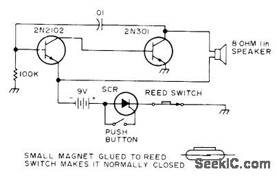
Tone oscillator driving loudspeaker is sealed into wood or plastic box, with reed switch mounted on one face of box and pushbutton of other switch projecting out through hole in box. Place DO NOT TOUCH label on button. When button is pushed despite yvaming, SCR latches and applies power to AF oscillator. Only way to turn off howling is to hold large permanent magnet against location of reed switch, to oppose field of magnet glued on switch and make reed contacts open. If mercury swhch is used in box in place of pushbut-ton, alarm goes off when box is picked up.-P.Walton, Now What Have I Done?, 73 Magazine, May 1975, p 81. (View)
View full Circuit Diagram | Comments | Reading(768)
SOUND_ACTIVATED_TAPE_SWITCH
Published:2009/7/7 20:38:00 Author:May
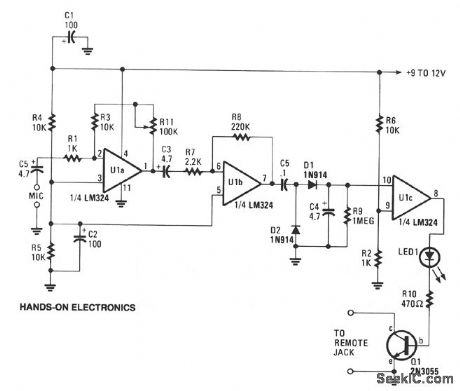
This circuit can cause a cassette recorder to automatically turn on and record when a sound or noise is present. Another use, is when the sound-activated switch is used to turn on a cassette player so that it operates as a burglar-alarm detector and sounder. Op amps U1a and U1b are connected in tandem to amplify the sounds picked up by the detector's mike. The amplified audio voltage, output at pin 7 of U1b, is fed to a voltage-doubler circuit, consisting of D1 and D2. The elevated voltage from the doubler circuit is input to the positive input of op amp U1c, which is operating as a simple comparator circuit. The other input of Ulc is connected to a voltage divider that sets the switching point for the dc signal voltage, to turn on when the signal level is greater than about 1.5 V. As the comparator switches on, its output at pin 8 becomes positive and supplies a forward bias to turn on D3 and Q1, which in turn, starts the recorder. The rc combination of C4/R9 sets the cassette's run time after the input sound has ceased, preventing the recorder from chopping-up or turning-off between closely spaced sounds or words picked up by the mike. The delay time is roughly 6 to 8 seconds. R11 sets the circuit's gain. Connect a low-impedance cassette mike to the amplifier's input, and connect the output of Q1 to the cassette's remote input or to the internal input and set the recorder to the record position. Talk and adjust the amplifier's gain with R11 for the desired sensitivity. (View)
View full Circuit Diagram | Comments | Reading(2676)
| Pages:977/2234 At 20961962963964965966967968969970971972973974975976977978979980Under 20 |
Circuit Categories
power supply circuit
Amplifier Circuit
Basic Circuit
LED and Light Circuit
Sensor Circuit
Signal Processing
Electrical Equipment Circuit
Control Circuit
Remote Control Circuit
A/D-D/A Converter Circuit
Audio Circuit
Measuring and Test Circuit
Communication Circuit
Computer-Related Circuit
555 Circuit
Automotive Circuit
Repairing Circuit