
Circuit Diagram
Index 969
PROPORTIONAL_CONTROL_FOR_OVEN
Published:2009/7/8 1:32:00 Author:May
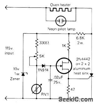
Thermistor RV1 and resistor-pot combination form voltage divider across 10-V zener, with output applied to UJT. Voltage across capacitor is ramp during positive half-eycles of AC Iine, slope of which is function of temperature and setting of 5K pot, When ramp reaches firing voltage of UJT, it turns on SCR and applies power to load, Negative half of AC input tums off SCR and cycle repeats. When oven temperature is low, SCR fires early in cycle to give more heat. When preset temperature is reached, SCR fires very late in cycle to compensate for heat lost by oven. Designed for 100'F environmental test chamber.-I. Math, Math's Notes, CQ, Sept. 1978, p 63 and 82-83.
(View)
View full Circuit Diagram | Comments | Reading(954)
SILICON_DIODE_SENSOR
Published:2009/7/8 1:30:00 Author:May
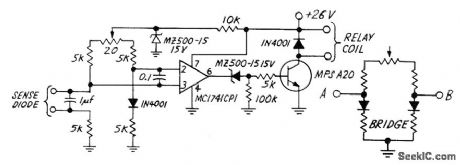
Ordinary silicon diode having temperature coefficient of about -2 mV/℃over wide temperature range serves for sensing temperature differentials up to ±10°F with resolution of about 0.3°F. Two diodes connected in resistor bridge provide voltage proportional to temperature difference at terminals A and B.Pot suppliesvariable offset current corresponding to presettable temperature offset range. Low output voltage of bridge is amplified by opamp such as Motorola MC1741 which gives output swing of 30 V for input change of 0.3 mV. Buffer transistor is added for handling Ioad such as motor control relay.- Industrial Control Engineering Bulletin, Motorola, Phoenix, AZ, 1973, EB-4.
(View)
View full Circuit Diagram | Comments | Reading(1398)
DIFFERENTIAL_THERMOMETER
Published:2009/7/8 1:18:00 Author:May
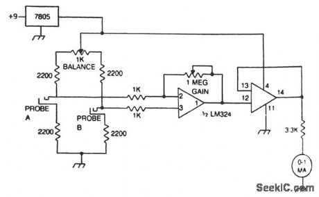
The differential thermometer uses two probes and shows the temperature difference between them, rather than the exact temperature. The thermometer uses a conventional meter as an indicator, and it covers a total range of 20 ° - 10 °low to 10 °high. (View)
View full Circuit Diagram | Comments | Reading(4641)
TESLA_COIL
Published:2009/7/8 1:11:00 Author:May
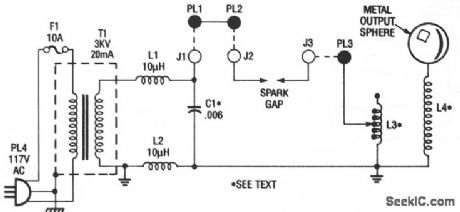


Power is fed to transformer T1, a small neon-sign transformer, which steps the voltage up to about 3000 Vac. The stepped-up output of T1 is fed through L1 and L2 and across C1, causing the capacitor to charge until enough power is stored in the unit to produce an arc across the spark gap. The spark gap, which momentarily connects C1 and L3 in parallel, determines the amount of current transferred between C1 and L3.The arcing across the spark gap sends a series of high-voltage pulses through L3, giving a sort of oscillated effect. The energy fed through L3 is transferred to L4 via the magnetic coupling between the two coils. Because of the turn ratio that exists between L3 and L4, an even higher voltage is produced across L4. Coil L4 steps up the voltage, which collects on the top-capacitance sphere. There, it causes an avalanche breakdown of the surrounding air, giving off a luminous discharge.The rotary spark gap is a simple add-on circuit for the Tesla Coil, consisting of a variable dc power supply and a small, 5000-rpm, dc motor. The circuit allows you to vary the output of the Tesla coil by adjusting the rotating speed of the motor. A rotary gap is far more efficient than a stationary gap, because the stationary gap could cut-out and require readjustment. (View)
View full Circuit Diagram | Comments | Reading(2074)
TWO_SIMPLE_TEMPERATURE_TO_TIME_CONVERTERS
Published:2009/7/7 23:55:00 Author:May
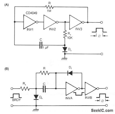


Both of these converters use CM0S inverters. Figure 105-1A shows a free-running circuit having both the pulse duration and pulse pause dependent on temperature of the diode DS. It can be used where a synchronization between the converter and something else is not required.
Figure 105-1B shows a one shot circuit that produces a pulse with its duration dependent of temperature of diode DS. The additional diode Df should have inverse current low enough to not influence the discharging process in the network rc when the INVA output is low. A silicon component or a GaAsP LED can be used.The converter is intended for a digital system producing a RADY pulse which disappears after the conversion process is ended. The pulse duration is approximately:where VD is the sensor diode forward voltage and VDD is the supply voltage of the CM0S chip.Resistance R must be much higher than RS A 0.1-μF capacitor can be applied in parallel with DS, if necessary, to repulse stray pickup and noise in a long cable. The circuits described can be used with a temperature sensitive resistor instead of the diode DS. (View)
View full Circuit Diagram | Comments | Reading(996)
160_W_LINEAR_SSB
Published:2009/7/7 23:48:00 Author:May
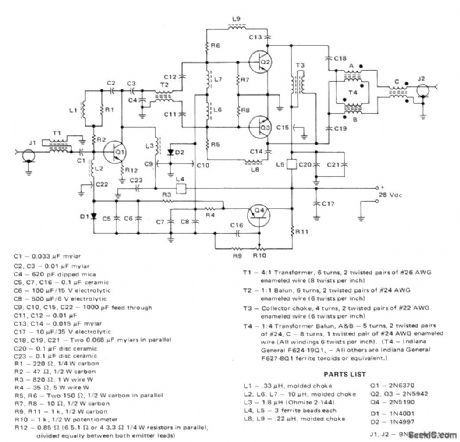
Designed for operation at fixed land location, using 28-VDC supply. Circuit covers 3-30 MHz band, using driver stage to providetotal power gain of about 30 dB, lf heatsinks are used, cooling fans are not normally re-quired because average power for speech operation is about 15 dB below peak levels.-H.Granberg, Broadband Linear Power Amplifiers Using Push-Pull Transistors, Motorola, Phoenix, AZ, 1974, AN-593, p 3. (View)
View full Circuit Diagram | Comments | Reading(813)
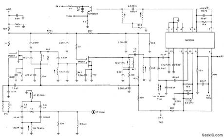
35_4_MHz_TUNABLE_IF_WITH_NOISE_BLANKING
Published:2009/7/7 23:47:00 Author:May

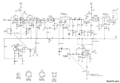
MC1550G is followed by Silicon General 563402T mixer that provides good conversion gain with very light oscillator loading. Mixer output is fed to 40673 amplifier that builds up noise spikes for blanker consisting of 1N60 diode gate and 40673 pulse amplifier. Blanker is fed from envelope detector that controls gate feeding FL1 dual ceramic filter providing IF selectivity. IF stage following blanker uses SD304 dual-gate MOSFET, transformer-coupled to ceramic filter FL2 at IF output. Article gives construction details.-R. Megirian, The Minicom Receiver, 73 Magazine, April 1977, p 136-149. (View)
View full Circuit Diagram | Comments | Reading(1687)
ISOLATED_TEMPERATURE_SENSOR
Published:2009/7/7 23:44:00 Author:May
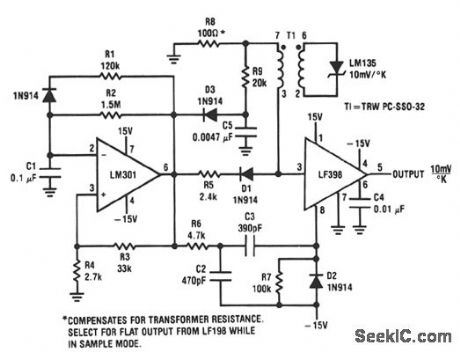
View full Circuit Diagram | Comments | Reading(2090)
O_63°C_TEMPERATURE_SENSOR
Published:2009/7/7 23:41:00 Author:May
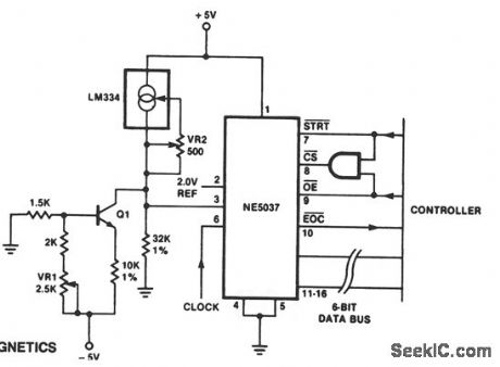
The temperature sensor provides an input to pm 3 of the NE5037 of 32 mV/°C。This 32 mV IS the value of one LSB for the NE5037. The LM334 is a three-terminal temperature sensor and provides a cur-rent of 1 μA for each degree Kelvin. The 32-KΩ resistor provides the 32 mV for each microamp through it, while the transistor bleeds off 273 μA of the temperature sensor (LM334) current. This bleeding lowers the reading by 273 K, thus converting from Kelvin to Celsius. To read temperature, conversion is started by sending a momentary low signal to pin 7 of the NE5037. When pin 10 of the NE5037 becomes low, conversion is complete and a low is applied to pin 9 of the NE5037 to read data on pins 11 and through 16. Note that this temperature data is in straight binary format. The controller can be a microprocessor in a temperature control application, or discrete circuitry in a simple temperature reporting application. (View)
View full Circuit Diagram | Comments | Reading(1662)
BROADBAND_MIXER
Published:2009/7/7 23:36:00 Author:May
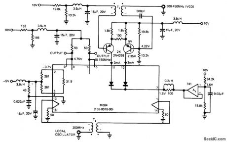
Uses Tektronix M084 multiplier as broadband mixer having linear output within -3 dB limit from 2 MHz to above150 MHz. Current-gain cell in multiplier takes advantage of logarithmic relationship between current and voltage in a semiconductor. Output function includes product of two Input signals,a300-450MHz swept VCO signal and a 300-MHz local oscillator signal.-M .Jaffe, Build a Low Cost Wideband Mixer with a Monolithic Multiplier, EDN Magazine. May 20,1975,p63-64. (View)
View full Circuit Diagram | Comments | Reading(1235)
THERMOCOUPLE_MULTIPLEX_SYSTEM
Published:2009/7/7 23:33:00 Author:May
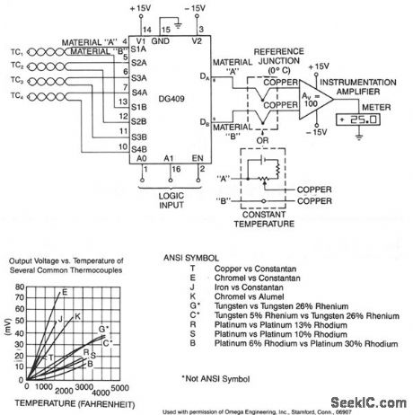
ANSI SYMBOL T Copper vs Constantan E Chromet vs Constantan J Iron vs Constantan K Chrornel vs Alumel G Tungsten vs Tungsten 26%Rhenium c TUNgsten 5% Rhenium vs Tungsten 26%Rhenium R Platlnum vs Platinum 13%Rhodium S Platinum vs Platinum 10%Rhodium B Platinum 6% Rhodium vs Platinum 30% Rhodium
Not ANSI Symbol
To decouple the sensors from the meter amplifter, either a reference junction at 0°C or a bucking voltage set at room temperature may be used. The latter method is simpler, but is sensitive to changes in ambient temperature The table above shows the output voltage vs temperature of several colmmon types of thermocouples. (View)
View full Circuit Diagram | Comments | Reading(1033)
STANDARD_PARALLEL_TRANSISTOR_OUTPUT_DOUBLER
Published:2009/7/21 7:01:00 Author:Jessie
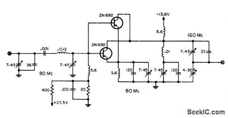
Input is tuned to 80 Mc and output to 160 Mc. Parallel tuned circuit with built-in trap is required in output circuit to suppress 80-Mc fundamental. Conversion power gain is 6 db. Maximum power is 650 mw.-W. A. Rheinfelder, Choosing the Best Transmitter Output Stage, EEE, 11:10, p 48-53. (View)
View full Circuit Diagram | Comments | Reading(819)
455_kHz_WITH_PRODUCT_DETECTOR_AND_BFO
Published:2009/7/7 23:32:00 Author:May
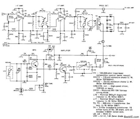
Used in 1.8-2 MHz communication receiver having wide dynamic range. Input comes from diode-switched bandpass filter giving choice of 400-Hz or 2.1-kHz bandwidths. Output for AGC amplifier is taken from primary of T3.AGO voltage, ranging from +2 V for minimum gain to +9 V for maximum gain, is applied to pins 7 of both IF opamps. Product detector uses quad 1N914A diodes. Varicap CR10 and R1 vary BF0 output from 453 to 457 kHz. Two-part artide gives all other circuits of receiver.-D.DeMaw, His Eminence-the Receiver, QST, Part 2-July 1976, p 14-17 (Part 1-June 1976, p 27-30). (View)
View full Circuit Diagram | Comments | Reading(1964)
LEVEL_SHIFTER_WITH_HIGH_CURRENT_DRIVE
Published:2009/7/7 23:31:00 Author:May
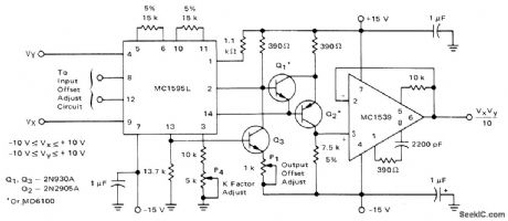
Motorola MC1539 opamp is used as source-follower output stage for three-transistor llevel shifter of MC1595L Iinear four-quadrant multiplier, to improve current drive capabilities. 0utput voltage is in range of ±10 V. Input offset adjusting circuits are 10K pots in series with 10K resistors between ±15 V, with 1K to ground from each side of paralleled pots.-E. Renschler, Analysis and Basic Operation of the MC1 595, Motorola, Phoenix, AZ, 1975, AN-489 p11. (View)
View full Circuit Diagram | Comments | Reading(929)
FOUR_OUADRANT_MULTIPLIER_SQUARER
Published:2009/7/7 23:26:00 Author:May
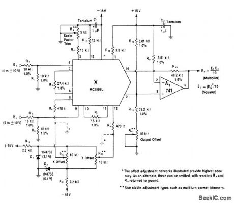
Basic1595 multiplier block and 741 current-to-voltage converter convert input voltages Ex and Ey to output equal to one-tenth of their product when connected as shown for multiplier use. To operate as squarer of Ex, connect pins 4 and 9 together and omit R5 and R6 at Ey input. Output is then one-tenth of square of Ex.-W. G. Jung, IC Op-Amp Cookbook, Howard W. Sams, Indianapolis, IN, 1974, p 255-257. (View)
View full Circuit Diagram | Comments | Reading(729)
Low_noise_TV_IF_system_with_two_FET_amplifiers
Published:2009/7/21 6:59:00 Author:Jessie
Low-noise TV IF system with two FET amplifiers (courtesy Motorola Semicon,-ductor Products Inc.). (View)
View full Circuit Diagram | Comments | Reading(924)
ELECTRONIC_HEAT_SNIFFER_
Published:2009/7/7 23:23:00 Author:May

Sensing element Q1 is a 2N3904 general-purpose npn transistor, although any general-purpose npn unit in a TO-92 style case will do. IC1, an LM334, supplies Q1 with a constant current that is independent of temperature. An LM324 quad op amp, IC2, forms a high input-impedance differential amplifier (IC2a, IC2b, and IC2c) with a gain of about 99. IC2d is used as a voltage comparator. When Q1 senses a rise or fall in temperature, the base-to-emitter voltage decreases. That decrease in voltage causes the input to IC2a at pin 3 to deviate from the reference voltage that's fed to IC2b at pin 5, which is set by potentiometers R5. The difference between the input and the reference is amplified by IC2c. That amplified voltage is fed to IC2d where it is compared to a control voltage set by potentiometer R13. The setting of R13 determines the threshold and is set at a point that's equal to the ambient temperature. The output of IC2d at pin 14 is fed to the base of transistor Q2. When the output of IC2d is high, LED1 lights and Q2 turns on. With Q2 turned on, a ground path through the transistor is provided for buzzer PB1.The circuit can be built on perforated construction board using point-to-point wiring. All components, except Q1, are mounted on the board. Transistor Q1 is mounted at the tip of the heat-sensing probe. (View)
View full Circuit Diagram | Comments | Reading(1264)
Color_TV_chroma_processor_using_an_ECG797_16_pin_QIP_with_AFPC_ACC_andkiller
Published:2009/7/21 6:52:00 Author:Jessie
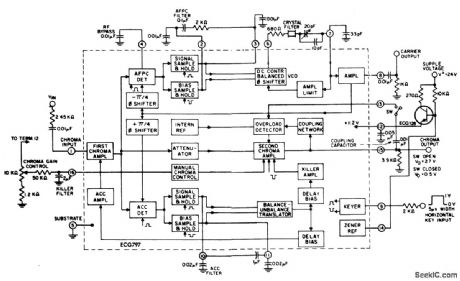
Color TV chroma processor using an ECG797 16-pin QIP with AFPC, ACC, andkiller (courtesy GTE Sylvania Incorporated). (View)
View full Circuit Diagram | Comments | Reading(807)
APPROXIMATING_ARC_TANGENTS
Published:2009/7/7 23:22:00 Author:May
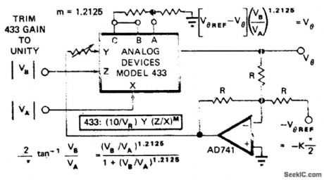
Analog Devices 433 multiplier/divider IC approximates arc tangent to 0. 75% Article presents mathematical basis for approximation used.-D.H Sheingold, Approximate Analog Functions with a Low-cost Multiplier/Divider.EDN Magazine,Feb,5.1973,p50-52. (View)
View full Circuit Diagram | Comments | Reading(719)
PIEZOELECTRIC_FAN_BASED_TEMPERATURE_CONTROLLER
Published:2009/7/7 23:18:00 Author:May
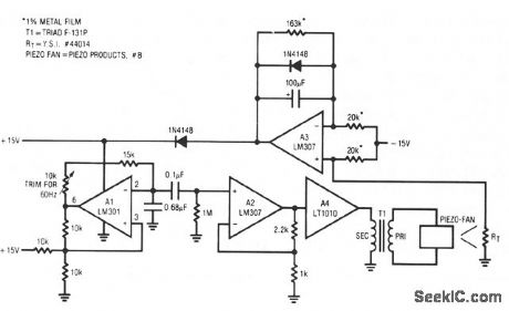
The fan employed is one of the new electrostatic type which is very retable, because it contains no wearing parts. These devices require high-voltage drive. When power is applied, the thermistor, located in the fan's exhaust stream, is at a high value. This value unbalances the A3 amplifier driven bridge. A1 receives no power and the fan does not run. As the instrument enclosure warms, the thermistor value decreases until A3 begins to oscillate. A2 provides isolation and gain, and A4 drives the transformer to generate high voltage for the fan. In this fashion, the loop acts to maintain a stable instrument temperature by controlling the fm's exhaust rate. The 100-μF time constant across the error amplifier pins is typical of such configurations. Fast time constants will produce audibly annoying hunting in the servo. Optimal values for this time constant and gain depend upon the thermal and airflow characteristics of the enclosure being controlled. (View)
View full Circuit Diagram | Comments | Reading(861)
| Pages:969/2234 At 20961962963964965966967968969970971972973974975976977978979980Under 20 |
Circuit Categories
power supply circuit
Amplifier Circuit
Basic Circuit
LED and Light Circuit
Sensor Circuit
Signal Processing
Electrical Equipment Circuit
Control Circuit
Remote Control Circuit
A/D-D/A Converter Circuit
Audio Circuit
Measuring and Test Circuit
Communication Circuit
Computer-Related Circuit
555 Circuit
Automotive Circuit
Repairing Circuit