
Circuit Diagram
Index 979
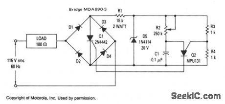
OVERVOLTAGE_INDICATOR
Published:2009/7/21 10:28:00 Author:Jessie
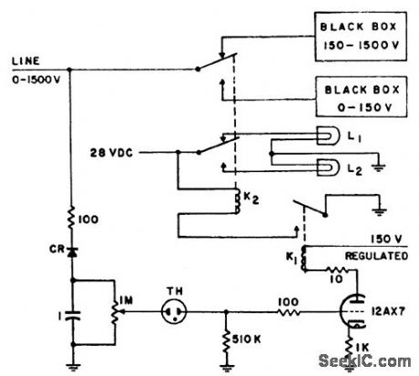
Routes line voltage automatically to black box designed to handle it. Potentiometer is set so neon lamp TH fires at 152 V. This applies high negative voltage to grid of tube, deenergizing relays K1 and K2 so line voltage is applied to upper black box. This condition also exists when system is first connected to line. After tube is warmed up, it switches to low-voltage box if line is below 152 V. Rectifier CR is any 2,000-V low-current rectifier, such as Sarkes Tarzian 126-100-H-Q. NE68 glow lamp TH must be in lightproof box; NE2 can be used only if suitably aged.-Overvoltage Indicator, Electronic Circuit Design Handbook, Mactier Pub. Corp., N.Y., 1965, p 124. (View)
View full Circuit Diagram | Comments | Reading(701)
PULSE_WIDTH_MODULATION_LAMP_BRIGHTNESS_CONTROLLER
Published:2009/7/7 9:57:00 Author:May
At half brightness, the lamp current is pulsed on and off (Fig. 50-12b) by the voltage developed across the resistor and capacitor at the current-sense output. Lamp current is sensed by the current-sense out-put. A simple pulse-width modulation lamp-brightness control circuit can also be built with the device. When the device powers up, the sense output is low, pulling the comparator output and the on input low, and turning the FET switch on. When the switch is on, current from the sense output charges the capaci-tor in the rc timing network to the 200-mV comparator threshold voltage. The comparator trips, turning the switch off. The charge then leaks off the capacitor, its voltage drops below 100 mV, and the FET is again turned on. The average current through the load is basically a function of the resistor value. The pulse-width modulation frequency on the other hand, is a function of the capacitor value. (View)
View full Circuit Diagram | Comments | Reading(821)
8_W_FLUORESCENT_LAMP_INVERTER
Published:2009/7/7 9:56:00 Author:May
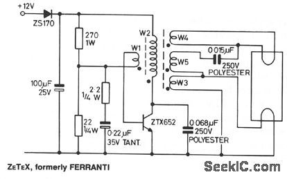
This circuit has been designed to drive an 8-W fluorescent lamp from a 12-V source using an inexpen-sive inverter based on the ZTX652 transistor. The inverter will operate from supplies in the range of 10 to 16.5 V, thus making it suitable for use in on-charge systems such as caravanettes as well as periodically charged systems, such as camping lights, outhouse lights, etc. Other features of the inverter are an inaudi-ble 20-kHz oscillator and reverse polarity protection. (View)
View full Circuit Diagram | Comments | Reading(1222)
LINE_VOLTAGE_OPERATED_AUTOMATIC_NIGHT_LIGHT
Published:2009/7/7 9:55:00 Author:May
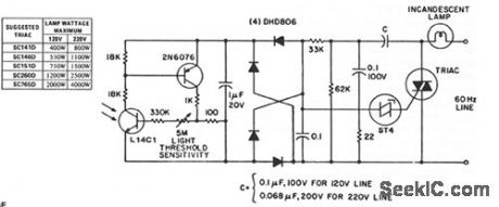
This circuit has stable threshold characteristics from its dependence on the photo diode current in the L14C1 to generate a base emitter voltage drop across the sensitivity setting resistor. The double phase shift network supplying voltage to the ST-4 trigger insures triac triggering at line voltage phase angles small enough to minimize RFI problems with a lamp load. This eliminates the need for a large, expensive inductor, contains the dV/dt snubber network, and utilizes lower voltage capacitors than the snubber ofrfi suppression network normally used. The addition of a programmable unijunction timer can modify this circuit to turn the lamp on for a fixed time interval each time its environment gets dark. Only the additions to the previous circuit are shown in the interest of simplicity. When power is applied to the lamp, the 2N6028 timer starts. Upon completion of the time interval, the H11C3 is triggered and turns off the lamp by preventing the ST-4 from triggering the triac. The SCR of the H11C3 will stay on until the L14C1 is illuminated and allows the 2N6076 to commutate it off. Because of capacitor leakage currents, tempera-ture variations and component tolerances, the time delay may vary considerably from nominal values. (View)
View full Circuit Diagram | Comments | Reading(771)
PHASE_CONTROL_1
Published:2009/7/7 9:53:00 Author:May
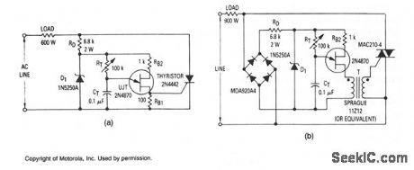
The most elementary application is a half-wave control circuit. The thyristor is acting both as a power control device and as a rectifier, providing variable power to the load during the positive half cycle and no power to the load during the negative half cycle. The circuit is designed to be a two terminal control which can be inserted in place of a switch. If full-wave power is desired as the upper extreme of this control, a switch can be added which will short circuit the SCR when RT is turned to its maximum power position. Full-wave control might be realized by the addition of a bridge rectifter, a pulse transformer, and by chang-ing the thyristor from an SCR to a TRIAC, shown in Fig 50-9b. In this circuit,RB1 is not necessary since the pulse transformer isolates the thyristor gate from the steady-state UJT current. Occasionally, a circuit is required to provide constant output voltage regardless of line voltage changes. Adding potentiorneter P1 to the circuits will provide an approximate solution to this problem. The potentiometer is adjusted to provide reasonably constant output over the desired range of line voltage. (View)
View full Circuit Diagram | Comments | Reading(1117)
SOLID_STATE_LIGHT_DISSOLVER
Published:2009/7/7 9:51:00 Author:May
The dinuning action is controlled by varying the amount of current passed through triac Q4 and, thus, the lamp plugged into ac receptacle SOl. Unijunction transistor Q3 operates as a relaxation oscillator whose output pulse frequency depends on how fast capacitor C2 recharges after firing. Transistors Q1 and Q2 furnish the charging current, with the R3/C1 and RI/R2/C1 time-constant networks controlling the turn-on and turn-off times. Inside IC1 is a LED, a detector, and a small triac. In circuit, the low-level pulses coming from Q3 make the LED in IC1 emit short bursts of light that are picked up and converted into electrical current pulses by the internal detector. This small current triggers the internal triac, which then outputs the pulses to the gate of power triac Q4, triggering it on so that it delivers current to the lamp. Potentiometer R4 serves as a master control of the pulse rate and provides both manual control and a limit in the brightness of the lamp plugged into SO1. Momentarily pressing 52 causes the lamp to instantly turn on. Choke L1 suppresses any spikes produced by the power triac and limits interference with AM radio reception. No safeguards against interference need to be made for FM and TV reception, since these media are immune to this type of noise. (View)
View full Circuit Diagram | Comments | Reading(644)
800_W_SOFT_START_LIGHT_DIMMER
Published:2009/7/7 9:50:00 Author:May
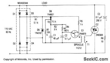
The zener provides a constant voltage of 20 V to unijunction transistor Q1, except at the end of each half-cycle of the input when the line voltage drops to zero. Initially, the voltage across capacitor C1 is zero and capacitor C2 cannot charge to trigger Q1. C1 will begin to charge, but because the voltage is low, C2 will be charged to a voltage adequate to trigger C1 only near the end of the half cycle. Although the lamp resistance is low at this time, the voltage applied to the lamp is low and the inrush current is small. Then the voltage on C1 rises, allowing C2 to trigger Q1 earlier in the cycle. At the same time, the lamp is being heated by the slowly increasing applied voltage. By the time the peak voltage applied to the lamp has reached its maximum value, the bulb has been heated sufficiently to keep the peak inrush current at a reasonable value. Resistor R4 controls the charging rate of C2 and provides the means to dim the lamp. Diode D6 and resistor R7 improve operation at low-conduction angles. (View)
View full Circuit Diagram | Comments | Reading(0)
TRIAC_LIGHT_DIMMER
Published:2009/7/7 9:48:00 Author:May
View full Circuit Diagram | Comments | Reading(174)
PHASE_CONTROL
Published:2009/7/7 9:48:00 Author:May
This circuit uses a PUT for phases control of an SCR. The relaxation oscillator formed by Q2 provides conduction control of Q1 from 1 to 7.8 ms or 21.6° to 168.5°. This constitutes control of over 97% of the power available to the load. Only one SCR is needed to provide phase control for both the positive and negative portion of the sine wave by putting the SCR across the bridge-composed of diodes D1 through D4. (View)
View full Circuit Diagram | Comments | Reading(1102)
LAMP_LIFE_EXTENDER
Published:2009/7/7 9:46:00 Author:May
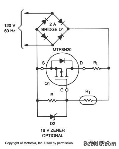
Lamp life can be extended by improving the conditions under which its filament is operated. This includes eliminating the inrush overcurrent surge and reducing the mechanical stress (vibration) on the filament caused by an ac source, The circuit shown controls the inrush current to the lamp without the 10 to 15 times-rated current stage that normally occurs when power is applied to a cold lamp. It does so by adjusting the inrush current over time to the inverse of the value normally experienced.RL is a standard tungsten lamp in the range of 15 to 250 W, R is 10-Ω and RT is a negative temperature coefflcient resistance that is initially 1.65 MΩ and decreases, by self-heating, to 150 KΩ in approximately 0.5 s. Use of the TMOS device allows high Ω values for R and RT, keeping drive power at a negligible level.This circuit has a number of advantages: very low power dissipation, long life, low-cost components, no significant effect on lamp ratings, negligible effect on efficiency, negligible RFI, and it can be used in hazardous environments. (View)
View full Circuit Diagram | Comments | Reading(730)
LIGHT_MODULATOR
Published:2009/7/7 9:44:00 Author:May
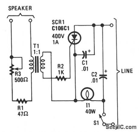
The lights seem to dance in time with the music. Line-voltage lamps of about 40 to 100 Mr do nicely. The current for the lamp is from an SCR. When low-level audio is present across T1, SCR1 is not triggered into conduction. A louder signal, how-ever, triggers the SCR so that the lamp lights and follows the sounds. Since SCR1 is operated by an alternating current, the rectifier moves out of the avalanche condition when the gate current is low. Potentiometer R3 lets you adjust the power reach-ing transformer T1, so that with normal operating volume, SCR1 triggers again and again, except dur-ing quiet passages. (View)
View full Circuit Diagram | Comments | Reading(808)
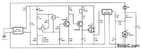
PSEUDORANDOM_SEQUENCER
Published:2009/7/7 9:43:00 Author:May
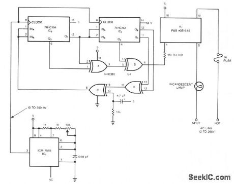
This pseudorandom sequencer drives a solid-state relay. If you power a low-wattage lamp from the relay, the lamp will appear to fiicker like a candle's flame in the wind; using higher-wattage lamps allows you to simulate the blaze of a fireplace or campfire. You can enhance the effect by using three or more such circuits to power an array of lamps.The circuit is comprised of an oscillator IC1 and a 15-stage, pseudorandom sequencer, IC2 through IC4. The sequencer produces a serial bit stream that repeats only every 32, 767 bits. Feedback from the sequencer's stages 14 and 15 go through IC4D and back to the serial input of IC2. Note the rc network feeding IC4C; the network feeds a positive pulse into the sequencer to ensure that it won't get stuck with all zeros at power-up. The leftover XOR gates IC4A and IC4B further scramble the pattern. The serial stream from IC4B drives a solid-state relay that features zero-voltage switching and can handle loads as high as 1 A at 12 to 280 Vac. (View)
View full Circuit Diagram | Comments | Reading(753)
HALOGEN_LAMP_DIMMER
Published:2009/7/7 9:41:00 Author:May
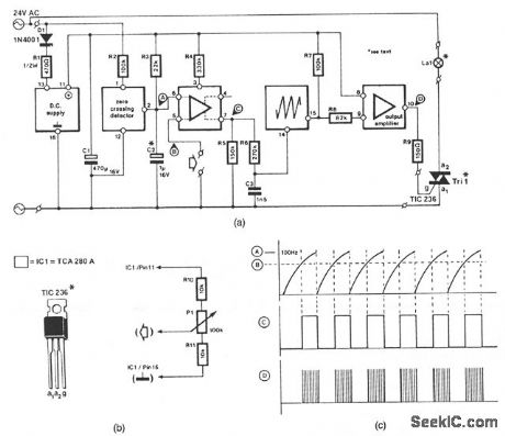
This circuit is suitable for fttting into slide projectors without a dimmer facility as with 24-Vac fed halo-gen lamps. With a few small alterations, it can also be used for dimming 12-V halogen lamps, but not those in a car, because these are fed from a dc source. The circuit shown in Fig. 50-1a is intended for operation from a 24-Vac supply, and can handle a lamp load of up to 150 W. For loads up to 250 W, the TIC236 should be replaced by a TIC246.Figure 50-1b shows detail of the connection of a potentiometer to the intensity control input of the TCA280A. Voltage divider R10-P1-R11 is fttted externally and can be fed from the stabilized voltage avail-able at pin 11 of IC1. The minimum and maximum intensities of the lamp are determined by R10 and R11, respectively. (View)
View full Circuit Diagram | Comments | Reading(2767)
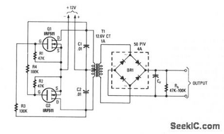
POWER_INVERTER
Published:2009/7/7 9:39:00 Author:May
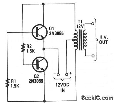
The transformer can be any 6.3 or 12.6 V type. Apply the 12-Vdc input so the positive goes to the transformer's center tap and the negative goes to the two transistor emitters. Any bridge-type rectifier and filter can be used at the output, if you need dc. (View)
View full Circuit Diagram | Comments | Reading(3896)
PRECISION_VOLTAGE_INVERTER
Published:2009/7/7 9:39:00 Author:May
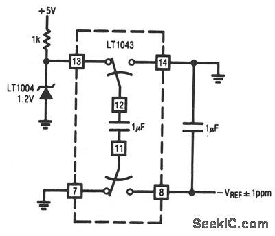
This circuit allows a reference to be inverted with 1 ppm accuracy, features high input impe-dance, and requires no trimming. (View)
View full Circuit Diagram | Comments | Reading(1234)
COMPLEMENTARY_OUTPUT_VARIABLE_FREQUENCY_INVERTER
Published:2009/7/7 9:38:00 Author:May
U1 is a 4060 12-stage binary ripple counter that is used as a free-running oscillator; its frequency of oscillation is: 1/2.2 C1R2. The output of U1 is applied to U2, a 14-stage binary ripple counter that pro-vides square-wave outputs of 1/2, 1/4, 1/g, and 1/16 of the clock frequency. These signals are combined in U3 and U4 to provide a complementary drive for Q1 and Q2.Outputs from U3 and U4 are ac-coupled to Q1 and Q2 via C2 and C4, respectively. R3 and R4 adjust the gate drive to Q1 and Q2. Q1 and Q2 alternately draw current through opposing sides of the primary to synthesize an ac input voltage at a given frequency. Only one side of the primary of T2 is driven at one time, so maximum power output is half of the transformer rating. (View)
View full Circuit Diagram | Comments | Reading(1097)
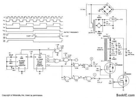
MEDIUM_POWER_INVERTER
Published:2009/7/7 9:36:00 Author:May
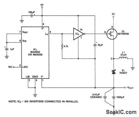
In this circuit, a CMOS inverter, such as the CD4069, is used to convert the open drain L, output to a signal suitable for driving the gate of an external P MOSFET The MTP8P03 has a gate threshold voltage of 2.0 V to 4.5 V, so it will have a relatively high resistance if driven with only 5 V of gate drive. To increase the gate drive voltage, and thereby increase efficiency and power handling capability, the negative supply pin of the CMOS inverter is connected to the negative output, rather than to ground. Once the circuit is started, the P MOSFET gate drive swings from + 5 V to - VOUT . At start up, the - VOUT is one Schottky diode drop above ground and the gate drive to the power MOSFET is slightly less than 5 V. The output should be only lightly loaded to ensure start up, since the output power capability of the circuit is very low until - VOUT is a couple of volts.This circuit generates complementary output signals from 50 to 240 Hz. Digital timing control ensures a separation of 10 to 15° between the fall time of one output and the rise time of the complementary out-put.The digital portion of inverter U1 to U4 controls the drive to Q1 and Q2, both MTE60N20 TMOS devices. These devices are turned on alternately with 11.25°separation between complementary out-puts. A +12-V supply for CMOS gates U1 to U4 is developed by T1, D3, D4, C7, and U6. The power supply for the TMOS frequency generator is derived from the diode bridge, U5, and capacitor C7; it is applied to the center tap of T2. (View)
View full Circuit Diagram | Comments | Reading(1176)
SECONDARY_EMISSION_PENTODE_TRIGGER
Published:2009/7/21 9:04:00 Author:Jessie
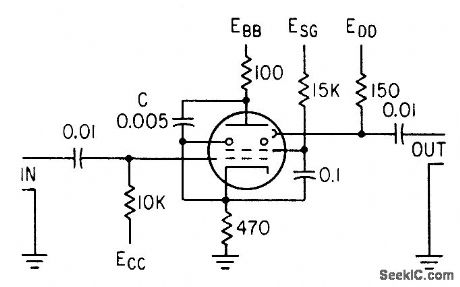
Produces positive output pulse across dynode loud each time it is triggered by positive grid pulse. Used in high-speed, short-duration pulse work.-E. J. Martin, Jr., How to Use the Secondary-Emission Pentode, Electronics, 33:41, p 60-63. (View)
View full Circuit Diagram | Comments | Reading(719)
POWER_MOSFET_INVERTER
Published:2009/7/7 9:33:00 Author:May
This inverter can deliver high-voltage ac or dc, with a rectifier and filter, up to several hundred volts. The secondary and primary of T1-a 12.6 to 440 V power transformer, respectively-are reversed; e.g., the primary becomes the secondary and the secondary becomes the primary. Transistors Q1 and Q2 can be any power FET. Be sure to heat sink Q1 and Q2. Capacitors C1 and C2 are used as spike suppressors. (View)
View full Circuit Diagram | Comments | Reading(2249)
Color_TV_chroma_processor_with_ACC_color_killer_and_an_injection_lock_reference_system
Published:2009/7/21 8:58:00 Author:Jessie
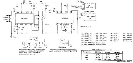
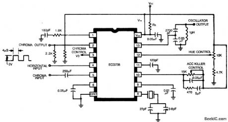
Color TV chroma processor with ACC, color killer, and an injection lock reference system. fypical power supply voltage is 9 to 11.5 volts. Hue control range is 100 degrees. The oscillator output signal is 180 mV PMS (courtesy GTE Sylvania Incorporated). (View)
View full Circuit Diagram | Comments | Reading(979)
| Pages:979/2234 At 20961962963964965966967968969970971972973974975976977978979980Under 20 |
Circuit Categories
power supply circuit
Amplifier Circuit
Basic Circuit
LED and Light Circuit
Sensor Circuit
Signal Processing
Electrical Equipment Circuit
Control Circuit
Remote Control Circuit
A/D-D/A Converter Circuit
Audio Circuit
Measuring and Test Circuit
Communication Circuit
Computer-Related Circuit
555 Circuit
Automotive Circuit
Repairing Circuit