
Circuit Diagram
Index 975
MODEL_TRAIN_SWITCHING
Published:2009/7/7 21:58:00 Author:May
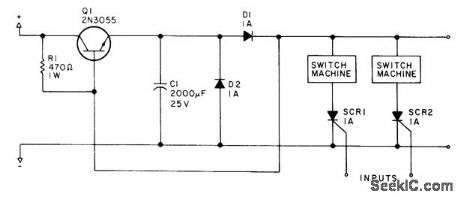
individual SCRs are triggered by logic-level signals independently to initiate discharge of large capacitor C1 through solenoid of model railroad tracks witch.-D. W. zimmerli,Two Hobbies:Model Railroading and Computing,Kilobaud Aug1978,p 62-68. (View)
View full Circuit Diagram | Comments | Reading(1001)
PRECISION_SQUARER
Published:2009/7/7 21:57:00 Author:May
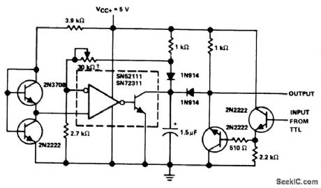
Circuit using differential comparator IC accepts input from TTL anddelivers square of input signal voltage to output. Adjust 30K pot to set clamp level. - The Linear and Interface Circuits Data Book for Design Engineers, Texas Instruments, Dallas, TX, FROM 1973, p 6-116. (View)
View full Circuit Diagram | Comments | Reading(1327)
XY÷Z_CIRCUIT
Published:2009/7/7 21:54:00 Author:May

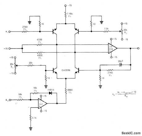
Developed for controlling amplitude of video signal from photodiode ary over 2 to 1 range. Circuit provides 3-dB band-width of 3 MHz, using CA3046 transistor array combined with LM318 opamp connected as analog divider, with half of 747 opamp sewing as current source. Article covers initial adjustments of circuit. Basic circuit may be used as full XY ÷ Z multiply/divide element with differential bipolar signals on one numerator input.-A. R. Kopp, An Analog Multiplier/Divider Circuit, EDN Magazine, May 5, 1973, p 74-75.
(View)
View full Circuit Diagram | Comments | Reading(1831)
ADD_ON_TELEPHONE_HOLD_BUTTON
Published:2009/7/7 21:52:00 Author:May
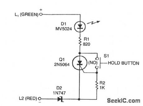
A sensitive-gate SCR provides a line-holding current of 20 to 40 mA, depending on loop resistance. It also lights an LED to give the user a positive indication that the telephone line is on hold. The 20 to 40 mA should prove sufficient to hold the majority of lines, but it might require increasing-by decreasing the size of R1-in individual instances. When any receiver in the same loop is lifted, the low impedance of the offhook telephone set shunts holding current away from the SCR, thereby releasing the line and extinguishing the LED. Zener diode D2 ensures that the line-holding current drops below the SCR's minimum conduction current. If the calling party tires of waiting on hold and hangs up, the release of the central-office relays from the calling side also releases the line from the hold mode. (View)
View full Circuit Diagram | Comments | Reading(740)
SCOER_DISPLAY
Published:2009/7/7 21:52:00 Author:May
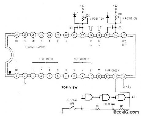
National 5841 IC is used for display of video game scores on TV receiver, as well as for time and channel number displays.Properly conditioned H and V pulses must be applied to pins 18 and 19 to interface TV. Output video on pin 15 must be buffered and summed into existing video inside TV set. Display position is controlled by H and V pots. Horizontal display size depends on clock frequency.Grounding M input gives only channel number.Positive voltage at M gives both channel and time. Grounding D input provides 5-slot time display, while positive D input gives 8-slot time display. Channel inputs are applied continuously in negative-logic form, with time inputs multiplexed externally.-D. Lancaster, CMOS Cookbook, Howard W. Sams, Indianapolis, IN, 1977, p 158. (View)
View full Circuit Diagram | Comments | Reading(1086)
ASUP2_SUP_BSUP2_SUP
Published:2009/7/7 21:48:00 Author:May
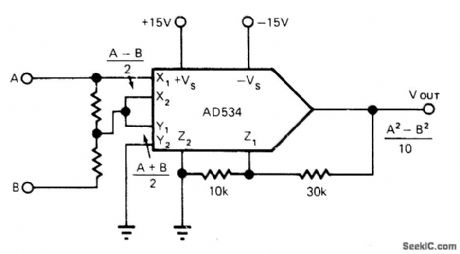
Transfer function Vour = (A2-B2)/10 is easily generated by AD534 analog multiplier.Differential inputs on Z terminals permit addition of feedback attenuator to decrease scale factor (or increase signal gain) from 40 to nominal value of 10. Feedback attenuation increases output offset proportionally; to make offset adjustment, connect 4.7-megohm resistor between Z1 and wiper of 50K pot connected across power supplies.-R. Frantz, Analog Multipliers-New IC Versions Manipulate Real-World Phenomena with Ease, EDN Magazine, Sept. 5, 1977, p 125-129. (View)
View full Circuit Diagram | Comments | Reading(893)
COIN_FLIPPER
Published:2009/7/7 21:47:00 Author:May
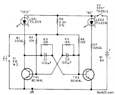
One of LEDs comes on when S1 is pressed, to simulate tossing of coin. LEDs can be labeled HEADS and TAILS if desired. Transistor types are not critical. For true random results, voltage between collectors of transistors should be 0 V with S2 closed and S1 open.-Circuits, 73 Magazine, June 1975, p 161. (View)
View full Circuit Diagram | Comments | Reading(0)
The_ECG_1064_chip
Published:2009/7/21 7:29:00 Author:Jessie
The ECG 1064 chip(see page 651).
(View)
View full Circuit Diagram | Comments | Reading(716)
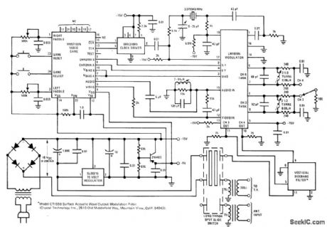
VIDEO_MODULATOR
Published:2009/7/7 21:44:00 Author:May
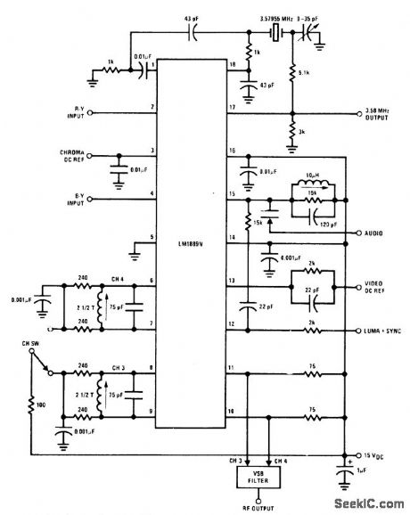
National LM1889N serves to interface dudio, color difference, and luminance signals to antenna terminals of TV receiver. Circuit allows video information from video games, test equipment, videotape reorders, and similar sources to be displayed on black-and-white or color TV receivers. LM1889N consists of sound subcarrier oscillator, chroma subcarrier oscillator, quadrature chroma modulators, and RF oscillators and modulators for two low VHF channels.- MOS/LSl Databook, National Semiconductor, Santa Clara, CA, 1977, p 4-48-4-49. (View)
View full Circuit Diagram | Comments | Reading(3971)
PARALLEL_TELEPHONE_CONNECTION
Published:2009/7/7 21:42:00 Author:May
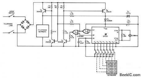
When the handset is lifted and power is applied to the circuit, Q2 is fed base current through R2, which in tum drives Q1. C2 is charged via R3 in series with D1 to (VZ1 - 0.7) V. When the minimum operating VDD voltage is reached, power on reset occurs via the rc network of C1 and R8. Q2 is maintained in the on condition by G1, while Q3, and hence Q4, are held off by G2. The DF320 network appears in parallel with the telephone as an impedance more than 10 KΩ in the standby condition with the telephone network connected in circuit through Q1. On recognition of the first keyed digit, the DF320 clock is started. M1 then goes to logic 1 causing Q2 and Q1 to turn off, and Q3 and Q4 to turn on. Hence, the majority of the line loop current now flows through Q4 and Z1. When impulsing occurs, Q3 and Q4 are turned off by DP acting on G2. Line loop current is then reduced to approximately 50 μA taken through R2, R4, and G2 in series. When dialing in, complete M1 goes to logic O, causing the telephone network to be reconnected. The DF320 then returns to the static standby condition. If the line loop is interrupted by the cradle switch during dialing, impulsing will continue until C2 discharges to a voltage, such that R8 pulls CE to logic O, causing the DF320 to reset. The diode bridge protects the network from line polarity reversal. (View)
View full Circuit Diagram | Comments | Reading(1310)
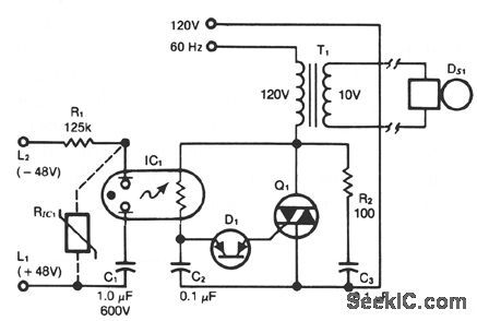
Triac_AC_static_contactor
Published:2009/7/21 7:29:00 Author:Jessie
Triac AC static contactor (courtesy Motorola Semiconductor Products Inc.). (View)
View full Circuit Diagram | Comments | Reading(693)
MULTIPLEXING_BCD_SWITCHES
Published:2009/7/7 21:40:00 Author:May
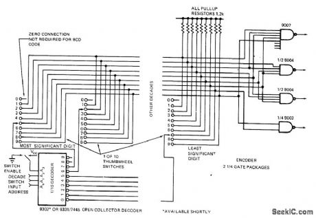
Multiplexing technique reduces number of interconnections between thumbwheel switches and counters, displays, or industrial control equipment being programmed remotely Ten decades of BCD switches require only 10 interconnections, as compared to 50 without multiplexing, All 10outputs of low-cost single-pole decade switches are paralleled. with wiper arm connections being brought out separately Parallel outputs are fed into simple encoder using four NAND gates to generate4-bit BCD output code. Wiper of each switch is addressed from active low open-collector decoder. In operation,3-bit input address determines which decade switch is addressed, and switch position then determines which encoder NAND gates are activated.-E. Breeze, Putting the, ”Thumb″ on Thumbwheel Switch Multiplexing, EDN Magazine, Aug,1,1972, p56. (View)
View full Circuit Diagram | Comments | Reading(1551)
223_MC_TELEMETRY_TRANSMIITER
Published:2009/7/21 7:28:00 Author:Jessie
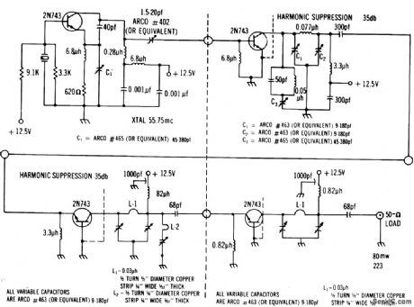
Crystal-controlled Colpitts delivers 10 mw to first doubler. Second doubler has trap to eliminate 11.5-Mc fundamental. Power output to final is about 45 mw at 223 Mc. Class C final delivers 100 mw to 50-ohm load.-Texas Instruments Inc., Solid-State Communications, McGraw-Hill, N.Y., 1966, p 326. (View)
View full Circuit Diagram | Comments | Reading(700)
DICE_OR_ROULETTE_RUNDOWN
Published:2009/7/7 21:39:00 Author:May
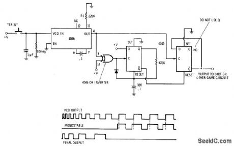
4046 PLL connected as VCO is set at twice desired maximum rate for dice or roulette-wheel counters. Pressing spin button momentarily to start action charges 1-uF capacitor to sypply voltage and jumps VCO to highest frequency. Output frequency then decreases rapidly as capacitor is discharged by 10megohm resistor. Output is stopped by using retriggerable mono to drive other half of 4013 dual D flip-flop. When frequency drops below value at which monotimes out, mono resets flip-flop and holds it to stop display.-D. Lancaster, CMOS Cookbook, Howard W. Sams, Indianpolis, IN, 1977, p 252-254. (View)
View full Circuit Diagram | Comments | Reading(3291)
OPTICALLY_INTERFACED_RING_DETECTOR
Published:2009/7/7 21:38:00 Author:May
This ring detector, utilizing a neon-LDR (light-dependent resistor) optocoupler, simplifies interfacing with telephone lines. (View)
View full Circuit Diagram | Comments | Reading(831)
PULSE_DIALING_TELEPHONE
Published:2009/7/7 21:36:00 Author:May

The TP5700 or TP5710 can reduce the number of components required to build a pulse-dialing telephone, as shown. The usual current source can be eliminated by using the VREG1 output to power a TP50982A low-voltage (1.7 V) pulse dialer via a blocking diode. A low forward-voltage drop diode such as a Schottky type is necessary because VREG1 is used in its nonregulated mode and its output voltage might fall to 2 V on a 20-mA loop. A 100-μF decoupling capacitor is required to hold up the pulse dialer supply voltage during dialing. This capacitor will take about one second to charge up when the telephone is first connected to the line, but thereafter, the 20-MΩ resistor, required to retain the last-number dialed memory, will keep this capacitor charged. Partial muting is obtained by directly connecting the N-channel opendrain mute output of the pulse dialer to the RCV in pin on the speech circuit. A fully muted pulse dialer design requires the use of a shunt-mode dialer, such as the TP50981A or TP50985A. (View)
View full Circuit Diagram | Comments | Reading(3281)
HOCKEY_TENNIS_HANDBALL
Published:2009/7/7 21:34:00 Author:May
Uses National have sound. MM57100 TV game chip to provide logic for generatingbackgrounds, paddles, ball, and dig ital scoring Circuit generates all necessary timing (sync, blanking, and burst) to interface with interface directly to antenna terminals of set.-MM57100 TV game chip to provide Iogic for ing (sync, blanking, and burst) to interface with circuit of standard TV receiver. With addition ofchroma, audio, and RF modulator, circuit will interface directly to antenna terminals of set.-''MOS/LSI Databook, National Semiconductor,Santa Clara, CA, 1977, p 4-37-4-47. (View)
View full Circuit Diagram | Comments | Reading(1023)
PHOTOELECTRIC_AC_POWER_SWITCH
Published:2009/7/7 21:32:00 Author:May
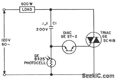
For a dark photocell, high resistance, the voltage across the diac rises rapidly with the line voltage due to the current through C1, triggering the diac early in the cycle.When the photocell resistance is less than about 2000 Ω,the drop across it is limited to less than the diac triggering voltage,and the load power is shut off. (View)
View full Circuit Diagram | Comments | Reading(1778)
SUN_TRACKER
Published:2009/7/7 21:29:00 Author:May
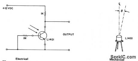
In solar cell array applications and solar instrumentation, it is desirable to monitor the approximate position of the sun to allow efficient automatic alignment. The L14G1 lens can provide about 15° of accuracy in a simple level sensing circuit, and a full hemisphere can be monitored with about 150 phototransistors. The sun provides = 80 mW/cm2 to the L14G1 when on the centerline. This will keep the output down to≤0.5 V for θ≤7.5°. The sky provides ≈0.5 mW/cm2 to the L14G1 and will keep the output greater than 10 V when viewed. White clouds viewed from above can lower this voltage to ≈5 V on some devices. This circuit can directly drive TTL logic by using the 5-V supply and changing the load resistor to 430 Ω. Different bright objects can also be located with the same type of circuitry simply by adjusting the resistor values to provide the desired sensitivity. (View)
View full Circuit Diagram | Comments | Reading(4065)
SIMPLE_TOUCHTONESUPTM_SUP_GENERATOR
Published:2009/7/7 21:29:00 Author:May
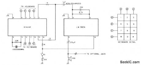
The oscillator is a Motorola MC14410CP chip using a 1-MHz crystal. The chip generates both the high and low tones, feeding the energy to the amplifier through 1-K resistors and the 1-μF capacitor. Values for the output resistors can vary from a few hundred Ω to about 60 KΩ. The value of the resistor shunting the crystal can vary from about 3 to 15 MΩ. The amplifier consists of an LM-380N. (View)
View full Circuit Diagram | Comments | Reading(767)
| Pages:975/2234 At 20961962963964965966967968969970971972973974975976977978979980Under 20 |
Circuit Categories
power supply circuit
Amplifier Circuit
Basic Circuit
LED and Light Circuit
Sensor Circuit
Signal Processing
Electrical Equipment Circuit
Control Circuit
Remote Control Circuit
A/D-D/A Converter Circuit
Audio Circuit
Measuring and Test Circuit
Communication Circuit
Computer-Related Circuit
555 Circuit
Automotive Circuit
Repairing Circuit