
Circuit Diagram
Index 976
SOLAR_TRIGGERED_SWITCH
Published:2009/7/7 21:28:00 Author:May

View full Circuit Diagram | Comments | Reading(715)
_LIGHT_CONTROLLED_ONE_SHOT_TINER
Published:2009/7/7 21:27:00 Author:May
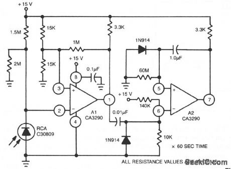

This circuit uses A1 of the CA3290 BiMOS dual voltage comparator to sense a change in light diode current. A2, a one-shot timer, is triggered by the A1 output. If the light source to the photodiode is interrupted, the circuit output switches to a low state for approximately 60 s.
(View)
View full Circuit Diagram | Comments | Reading(690)
Color_TV_AFT_circuit
Published:2009/7/21 7:28:00 Author:Jessie
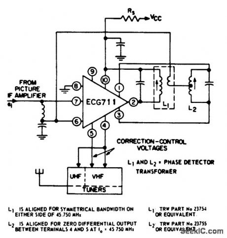
Color TV AFT circuit. The supply is +30 volts, resistor Rs is 1.5K, the bypass capacitor between pin 10 and ground is 0.001 μF, the capacitor across L1 is 91 pF, the capacitor across L2 is 68 pF, the series coil and capacitor at pins 6 and 7 are 3.3 μH and 0.001 μF and the input frequency at 45.75 MHz (courtesy GTE Sylvania Incorporated). (View)
View full Circuit Diagram | Comments | Reading(948)
WARNING_LIGHTAND_MARKER_LIGHT
Published:2009/7/7 21:26:00 Author:May
A flashing light of high brightness and short duty cycle is often desired to provide maximum visibility and battery life. This necessitates using an output transistor, which can supply the cold filament surge current of the lamp while maintaining a low saturation voltage. The oscillation period and flash duration are determined in the feedback loop, while the use of a phototransistor sensor minimizes sensitivity varia-tions. (View)
View full Circuit Diagram | Comments | Reading(912)
1_kHz_N_PATH_NOTCH_FILTER
Published:2009/7/7 21:24:00 Author:May
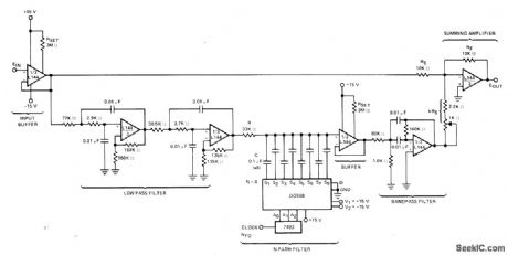
Combination of DG508 eight-channel CMOS multiplexer with low-pass and bandpass active filters provides 1-kHZ notch filter having Q of 1330 and 3-dB bandwidth of 0.75 Hz at 1 kHz. Low-pass filter introduces 180° phase shift at 1 kHz. Amplifier sums original signal in phase-shifted bandpass output from N-path filter, canceling 1-kHz components in original signal to produce desired notch characteristic.-″Analog Switches and Their Applications, SiIiconix. Santa Clara,GA,1976,p5-18-5-20. (View)
View full Circuit Diagram | Comments | Reading(2312)
LIGHTED_DISPLAY_BRIGHTNESS_CONTROL
Published:2009/7/7 21:24:00 Author:May
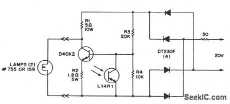
This circuit provides a very low cost method of controlling light levels. Circuit power is obtained from a relatively high source impedance transformer or motor windings, normally used to drive the low-voltage lamps used in these functions. It should be noted that the bias resistors are optimized for the 20-V, 30-Ω source, and they must be recalculated for other sources. The L14R1 is placed to receive the same ambient illumination as the display and should be shielded from the light of the display lamps. The illumination level of lighted displays should be lowered as the room ambient light dims, to avoid undesirable or unpleasant visual effects.
(View)
View full Circuit Diagram | Comments | Reading(650)
LIGHT_LEVEL_DETECTOR
Published:2009/7/7 21:22:00 Author:May
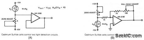
If R, the sensor matching resistor, is equal to the dark resistance of the cadmium sulfide cell, the amplifier output will range from 0 to≈ 2 as the light level ranges from dark to bright. The circuit in Fig. B operates similarly, but use the standard noninverting configuration instead of the voltage-follower configuration; this allows for variable gain. Although the dark resistance of the cadmium sulfide cell is only ≈7 KΩ, the principles of operation apply to other types of detectors which require the high-input impedance of the HA-5180 for reasonable linearity and useability. (View)
View full Circuit Diagram | Comments | Reading(744)
LIGHT_SENSITIVE_AUDIO_OSCILLATOR
Published:2009/7/7 21:21:00 Author:May
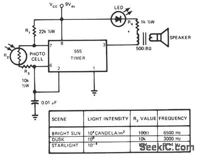
This circuit's frequency of oscillation increases directly with light intensity. The greater the light intensity, the higher the frequency of the oscillator. The 555 timer operates in the astable oscillator mode where frequency and duty cycle are controlled by two resistors and one capacitor. The capacitor charges through R1 and R2, and discharges through R2, a standard photo cell. Resistor R3 limits the upper frequency of oscillation to the audio range. The lower range of approximately 1 pps is set 'oy the value of R2, approximately 10-MΩ, with the photo cell almost totally dark.A loudspeaker provides audio output, and an LED is used as a pilot light that flashes when the frequency falls below about 10 to 12 Hz. Extremely sensitive, especially on the dark end of the photocell resistance range, the unit can detect lightning many miles away, providing a rapid frequency increase with each flash of lightning. When used with a flashlight at night, the device becomes a simple optical radar for the blind, showing angular direction to a light-reflecting object, as well as height and distance to the object when hand scanned back and forth.This light-sensitive audio oscillator can also serve as an audible horizontal level device by noting the position of a liquid bubble illuminated by a light source. Thus, you can sense fluid levels as well as the vibration state of a fluid surface level. (View)
View full Circuit Diagram | Comments | Reading(1032)
SERIES_TELEPHONE_CONNECTION
Published:2009/7/7 21:21:00 Author:May
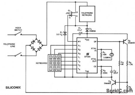
Here is a simple method of series connection into the telephone set suitable for PABX or short line applications. When the telephone handset is lifted, C1 is charged via Dl to (VZ1 - 0.7) V and DF320 power on reset occurs. When the first keyed digit is recognized, Ml goes to logic 1, muting the telephone network by switching on the low on resistance JFET Q1, and maximizing the line-loop current for impulsing. lmpulsing occurs through DP switching Q2, and hence Q3 turns off. Rapid discharge of C1 through Z1 is prevented during line break by blocking diode D1. When dialing is complete, the circuit returns to the static standby condition, and Q1 is switched off. The circuit reset, during a line interruption by the cradle switch, is for the parallel connection mode. (View)
View full Circuit Diagram | Comments | Reading(2531)
HEADS_TAILS_FLIPPER
Published:2009/7/7 21:18:00 Author:May
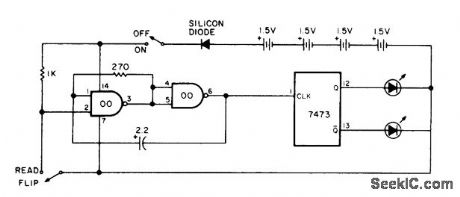
Uses only half of 7400 quad NAND gate as gated clock driving half of 7473 JK flip-flop. With power switch closed, LEDs representing heads and tails flash on and off at clock frequency, Closing FLIP switch stops clock randomly, leaving one LED on to give equivalent of tossing coin for heads/tails call.-G. Young,JK Flip-Flops and Clocked Logic, Kilobaud, July 1977, p 66-70 and 72-73. (View)
View full Circuit Diagram | Comments | Reading(1352)
OPTICAL_SENSOR_TO_TTL_INTERFACE
Published:2009/7/7 21:17:00 Author:May
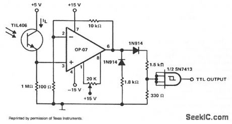
This circuit is designed to detect a low light level at the sensor, amplify the signal, and provide a TTL-level output. When the optical sensor detects low-level light, on condition, its output is small and must be amplified. An amp with very low input bias current and high input resistance must be used to detect the on condition. When sensor TlL406 is in the on condition, its output is assumed to be 250 nA (allowing a safety margin). This results in a 250-mV signal being applied to the noninverting input of amplifier OP-07.Because of the circuit configuration, the OP-07 provides a gain of 100 and its output is in positive saturation. The OP-07 output level is applied to a loading network that provides the basic TTL level. (View)
View full Circuit Diagram | Comments | Reading(3076)
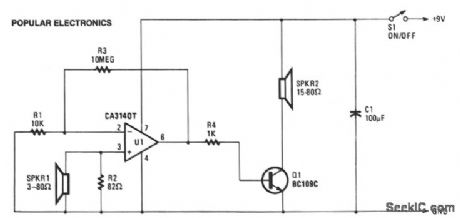
SPEAKERPHONE
Published:2009/7/7 21:17:00 Author:May
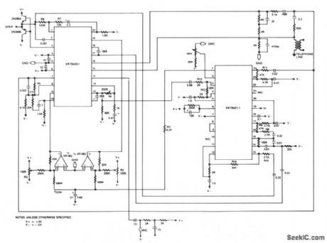
This circuit consists of two audio channels, a control circuit, and a hybrid interface circuit. The gain of each audio channel is controlled by the control circuitry, with the use of a voltage controlled amplifier (VCA). The inputs to the control circuit are obtained from each of the audio channels. The hybrid interface circuit performs three important functions. First, it couples the Tx channel signal to the telephone line. Second, it couples the signal on the telephone line to the Rx channels. And, finally, it cancels a majority of the TX signal that can couple into the Rx channel. The amount of TX signal that appears on the RX channel is called sidetone. (View)
View full Circuit Diagram | Comments | Reading(0)
LIGHT-CONTROLLED_LAMP_SWITCH
Published:2009/7/7 21:16:00 Author:May
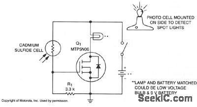
A school drama needed lamps that automatically turned on and off when spot lights did the same.Lamp switching had to be wireless, durable, dependable, simple and inexpensive. With stage and spot lights off, very little light falls on the CdS photocell, so its internal resistance is several megohms and R1 keeps the gate of Q1 at nearly zero volts, which keeps it off. When a spot or stage light hits the photocell, its resistance drops to several hundred ohms, raising Q1's gate voltage, which turns it on and applies power to the lamp. (View)
View full Circuit Diagram | Comments | Reading(994)
THREE_CHANNEL_FOR_DATA
Published:2009/7/7 21:15:00 Author:May
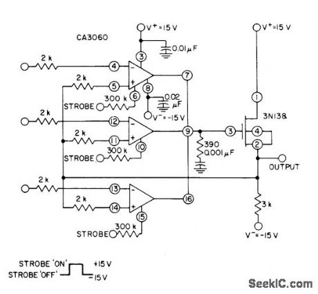
Each input channel uses CA3060 variable opamp as high-impedance voltage follower driving output MOSFET serving as buffer and power amplifier. Cascade arrangement of opamps with MOSFET provides open-loop voltage gain in excess of 100 dB.- Circuit Ideas for RCA Linear ICs, RCA Solid State Division, Somerville, NJ, 1977, p16. (View)
View full Circuit Diagram | Comments | Reading(733)
LOW_LIGHT_LEVEL_DROP_DETECTOR
Published:2009/7/7 21:15:00 Author:May
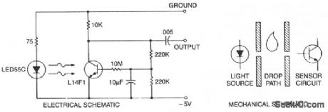
This self-biasing conftguration is useful any time small changes in light level must be detected, for example, when monitoring very low f1ow rates by counting drops of fluid. In this bias method, the photodarlington is dc bias stabilized by feedback from the collector, compensating for different photodarlington gains and LED outputs. The 10-μF capacitor integrates the collector voltage feedback, and the 10-MΩ resistor provides a high base-source impedance to minimize effects on optical performance. The detector drop causes a momentary decrease in light reaching the chip, which causes collector voltage to momentarily rise, generating an output signal. The initial light bias is small because of output power constraints on the LED and mechanical spacing system constraints. The change in light level is a fraction of this initial bias because of stray light paths and drop translucence. The high sensitivity of the photodarlington allows acceptable output signal levels when biased in this manner. This compares with unacceptable signal levels and bias point stability when biased conventionally, i.e., base open and signal output across the collector bias resistor.
(View)
View full Circuit Diagram | Comments | Reading(1101)
PLOP_FOR_GAMES
Published:2009/7/7 21:15:00 Author:May
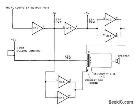
Section 1 of 7406 TTL hex inverter can be attached to output port and driven by program loop, to provide sound effects for computer games. When output port goes to logic1 (greater than +2 V). action of inverter is such that paralleled inverters 3 and 4 go to 0 and draw current through primary of T1, making loudspeaker produce single plopping sound.When outputport goes to 0, another plop is produced. If output port is switched between 0 and 1 fast enough, loudspeaker output will be tone at switching frequency.-D. Parks, Adding Plop to Your System, Kilobaud, May 1977, p 98. (View)
View full Circuit Diagram | Comments | Reading(826)
TIME_MULTIPLEXING_TWO_FM_CHANNELS
Published:2009/7/7 21:13:00 Author:May
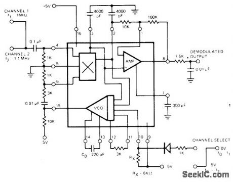
Digital programming capability of Exar XR-215 PLL IC makes possible time-multiplexing de-modulator between two FM channels, at 1.0 and 1.1 MHz. Channel-select logic signal is applied to pin 10, and both input channels are applied simultaneously to PLL input pin 4.- Phase-Locked Loop Data Book, Exar Integrated Systems, Sunnyvale, CA, 1978, p 21-28. (View)
View full Circuit Diagram | Comments | Reading(690)
FLAME_MONITOR
Published:2009/7/7 21:13:00 Author:May
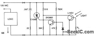
Monitoring a flame and directly switching a 120-V load is easily accomplished using the L14G1 for point sources of light. For light sources which subtend over 10°of arc, the L14C1 should be used and the illumination levels raised by a factor of 5. This circuit provides zero voltage switching to eliminate phase controlling. (View)
View full Circuit Diagram | Comments | Reading(763)
TELEPHONE_REPEATER
Published:2009/7/7 21:12:00 Author:May
View full Circuit Diagram | Comments | Reading(878)
LASER_DIODE_PULSERS
Published:2009/7/7 21:11:00 Author:May
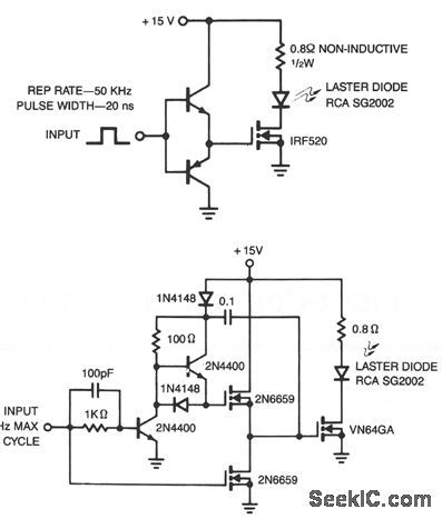
The laser diode pulser is a simple drive circuit capable of driving the laser diode with 10-A, 20-ns pulses. For a 0.1% duty cycle, the repetition rate will be 50 kHz. A complementary emitter follower is used as a driver. Switching speed is determined by the fT of the bipolar transistors used and the impedance of the drive source. A faster drive circuit is shown. It can supply higher peak gate current to switch the IRF520 very quickly. This circuit uses a MOSPOWER totem-pole stage to drive the high power switch.The upper MOSFET is driven by a bootstrap circuit. Typical switching times for this circuit are about 10 ns for both turn-on and turn-off.
(View)
View full Circuit Diagram | Comments | Reading(2519)
| Pages:976/2234 At 20961962963964965966967968969970971972973974975976977978979980Under 20 |
Circuit Categories
power supply circuit
Amplifier Circuit
Basic Circuit
LED and Light Circuit
Sensor Circuit
Signal Processing
Electrical Equipment Circuit
Control Circuit
Remote Control Circuit
A/D-D/A Converter Circuit
Audio Circuit
Measuring and Test Circuit
Communication Circuit
Computer-Related Circuit
555 Circuit
Automotive Circuit
Repairing Circuit