
Circuit Diagram
Index 978
8_CHANNEL_CRO_MULTIPLEXER
Published:2009/7/7 20:37:00 Author:May
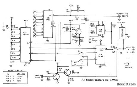
Simple adapter converts any single-trace oscilloscope into professional 8-channel model by multiplexing eight input signals into one output for vertical amplifier. Discrete voltages are picked off resistor divider chain sequentially and added to digital input signal so trace is shifted fast enough to produce eight individual traces. Addressing for 74151 digital multiplexer requires 3 bits of binary code to address all eight channels in sampling sequence. As each channel is sampled, its logic level (1 or 0) appears at pin 5 of 74151 for feed to vertical input of CRO. Developed for troubleshooting in digital circuits.-W. J. Prudhomme, Build an Eight Channel Multiplexer for Your Scope, Kilobaud, April 1977, p 29-32. (View)
View full Circuit Diagram | Comments | Reading(1923)
SOUND_ACTIVATED_SWITCH
Published:2009/7/7 20:33:00 Author:May
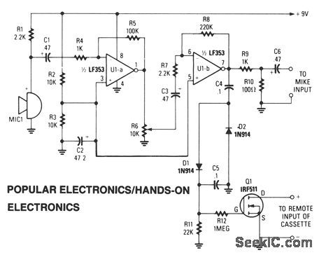
A sensitive electret microphone picks up the sound and feeds the signal to a two-stage amplifter circuit, consisting of U1a and U1b. The amplified output of U1b is fed to a voltage-doubler circuit (comprised of D1, D2, C4, and C5). The output of the doubler is input to the gate of Q1. When the dc voltage reaches the gate's threshold level, Q1 switches on, starting the recorder. Resistor R6 sets the circuit's sensitivity and should be experimented with to obtain the optimum adjustment. (View)
View full Circuit Diagram | Comments | Reading(0)
64_CHANNEL_TWO_LEVEL_HIGH_SPEED
Published:2009/7/7 20:33:00 Author:May
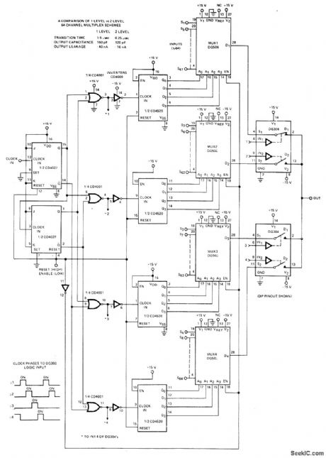
Foul DG506 16-channel multiplexers serve for first multiplexer level, and two DG304 high-speed dual analog switches serve in second level for switching DG506 outputs to single output of multiplexer. As one multiplexor is being sampled at output, other multiplexers are being switched to next address line; this shortens overall system transition time from 1.5μs to 0.25μs. Two-level system also lowers output node capacitance and output leakage. CMOS digital logic controls entire system.- Analog Switches and Their Applications, Siliconix, Santa Clara, CA, 1976, p 7.82-7-84. (View)
View full Circuit Diagram | Comments | Reading(703)
EXTENDED_PLAY_CIRCUIT
Published:2009/7/7 20:30:00 Author:May
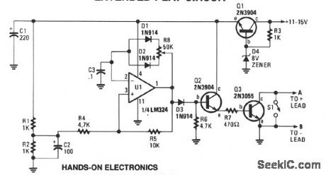
A single op amp-one of four contained in the popular LM324-is operating in a variable pulsewidth, free-running squarewave oscillator circuit, with its timed output driving two transistors that control the on/ off cycle of the tape-drive motor.The oscillator's positive feedback path holds the secret to the successful operation of the variable on/ off timing signal. The two diodes and pulsewidth potentiometer R8 allows the setting of the on and off time, without affecting the oscillator's operating frequency. One diode allows only the discharge current to flow through it and the section of R8 that it's connected to. The other diode, and its portion of R8, sets the charge time for the timing capacitor, C3. Since the recorder's speed is controlled by the precise off/on timing of the oscillator, a simple voltage-regulator circuit (Q1, R3, and D4) is included.Connecting the speed control to most cassette recorders is a simple matter of digging into the recorder and disconnecting either of the motor's power leads, the ground or common side might be best, and connecting the recorder through a length of small, shielded cable to the control circuit. In some recorders, a remote input jack is furnished to remotely turn on and off the recorder. Before going in and modifying a recorder with a remote jack, try connecting the circuit to the external remote input. (View)
View full Circuit Diagram | Comments | Reading(1577)
FOUR_CHANNEL_DIFFERENTIAL
Published:2009/7/7 20:28:00 Author:May
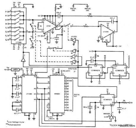
Low-speed high-accuracy data acquisition unit acquires analog input signal differentially with LF13509 IC and preconditions it through LF352 instrumentation amplifier having automatic zeroing circuit. Timing is provided by MM5863 12-bit A/D converter and lower MM74C74 flip-flop. Upper two flip-flops form 2-bit up counter for channel select. Instrumentation amplifier is zeroed at power-up and after each conversion. Maximum clock frequency depends on required accuracy and minimum zeroing time of instrumentation amplifier.- MOS/LSI Databook, National Semiconductor, Santa Clara, CA, 1977, p 5-2-5-22. (View)
View full Circuit Diagram | Comments | Reading(1234)
BATTERY_SPLITTER
Published:2009/7/7 20:23:00 Author:May
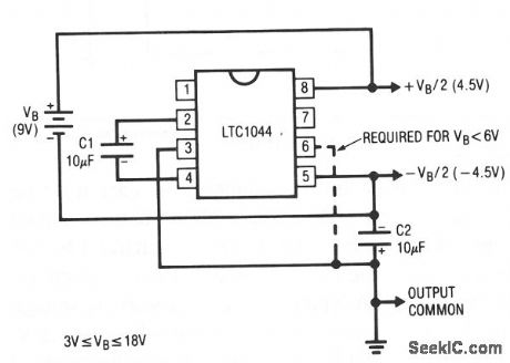
A common need in many systems is to obtain positive and negative supplies from a single battery. Where current requirements are small, the circuit shown is a simple solution. It provides symmetrical ±output voltages, both equal to one half the input voltage. The output voltages are referenced to pin 3, output common. If the input voltage between pin 8 and pin 5 exceeds 6 V, pin 6 should also be connected to pin 3, as shown by the dashed line.Higher current requirements are served by an LT1010 buffer. The splitter circuit can source or sink up to ±150 mA with only 5 mA quiescent current. The output capacitor, C2, can be made as large as necessary to absorb current transients. An input capacitor is also used on the buffer to avoid high frequency instability that can be caused by high source impedance. (View)
View full Circuit Diagram | Comments | Reading(614)
WIDEBAND_DIFFERENTIAL_INPUT
Published:2009/7/7 20:22:00 Author:May
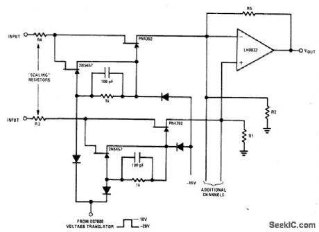
Circuit design using PN4392 FET switches driven by 2N5457 general-purpose FETs allows handling of high-frequency signals at toggle rates up to 1 MHz for multiplexing to any desired number of channels,- FET Databook, Nation Semiconductor, Santa Clara,CA,1977,p 6-26-6-36. (View)
View full Circuit Diagram | Comments | Reading(658)
BATTERY_CAPACITY_TESTER
Published:2009/7/7 20:20:00 Author:May

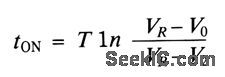
The test circuit gives an indication of the capacity remaining in a battery. By noting the time in seconds that the LED remains on after you depress the test switch S1. The circuit has proven reliable in testing NiCad-, carbon-, and alkaline-type batteries. Closing S1 activates the circuit by applying voltage from the battery under test. Voltage V1 jumps to a value V0= VRR3/(R2 + R3) when the switch closes and then increases with a time constant T = C1 (R2 + R3). The divider R4/R5 fixes V2. The reference circuit IC1 sets VR to approximately 2.5 V. The op amp's output remains high (LED on) until V1 rises to the level of V2, when the LED turns off. Calculate the on-time tON as follows:
(View)
View full Circuit Diagram | Comments | Reading(1120)
64_CHANNEL_TWO_LEVEL
Published:2009/7/7 20:15:00 Author:May
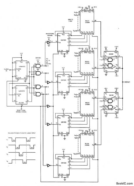
Two-level multiplexing system increases effective switching speeds when transmitting 64 analog signals on single transmission line. Four clock phases are generated with DM7473 2-bit counter that toggles on high-to-low dock edge. DM7400 NAND gates decode flip-flop outputs into required four clock phases. As clock phase goes from low tohigh state, DGt181 analog switch fed by it turns off and corresponding DM7493 4-bit binary counter is triggered to next address state for sampling of that input channel at output. Reset is used to set system for starting on first channel when power is applied.- Analog Switches and Their Applications, Siliconix, Santa Clara, CA, 1976, p 7-11-7-13. (View)
View full Circuit Diagram | Comments | Reading(947)
BFO_MULTIPLEXER
Published:2009/7/7 20:10:00 Author:May
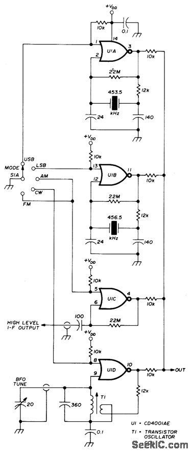
Signal 455-kHz multi-mode detection system using RCA CD4001AE quad NOR gate functions as upper-sideband or lower-sideband crystal oscillator, tunable BF0 for CW, or limiter of IF signal for FM or synchronous AM reception, Desired oscillator or limiter is gated on by grounding its digital control line with S1A. Multimode reception occurs when multiplexed output of oscillators and limiter is applied to product detector-J. Regula, BFO Multiplexor for a Multimode Detector, Ham Radio, Oct. 1975, p 52-55. (View)
View full Circuit Diagram | Comments | Reading(893)
THERMOELECTRIC_COOLING_CONTROL
Published:2009/7/21 21:22:00 Author:Jessie
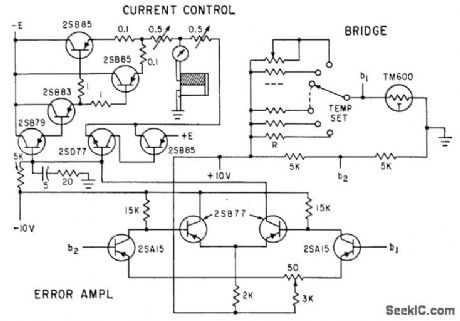
Temperature inside cooling chamber is sensed by thermistor bridge and bridge output is com pared with temperature-setting reference voltage. Difference voltage is amplified and fed to current control circuit of thermoelectric converter.-M. Nagata and Z. Abe, Thermoelectric Elements for Circuit Cooling, Electronics, 34:41, p 54-55. (View)
View full Circuit Diagram | Comments | Reading(1573)
ARC_PROTECTION_CIRCUIT
Published:2009/7/21 10:58:00 Author:Jessie
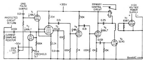
Circuit ignores desired peak pulse currents by sensing their coincidence with drive pulse, but fires trigger thyratton V6 and V7 in absence of drive pulse, to make thyratrons discharge power supply before breakdown and flashover of high-voltage electron device under test.-D. D. Mawhinney, Latest Thing in Arc-Protection Circuits, Electronics, 36:8, p 54-55. (View)
View full Circuit Diagram | Comments | Reading(832)
LIFESAVER
Published:2009/7/21 10:55:00 Author:Jessie
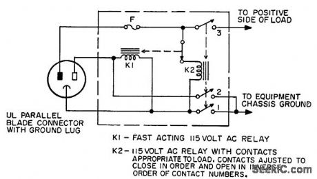
Used with transformerless line-operated equipment to minimize possibility of chassis being hot. Relays are so arranged that they automatically search for proper relationship of voltages between hot, neutral and ground terminals before power is applied to equipment. Only limitation is failure to protect against rare fault in which both neutral and conduit ground are at line potential with respect to earth ground.-R. E. Pafenberg, Lifesaver Circuit, EEE, 10:7, p 26-27. (View)
View full Circuit Diagram | Comments | Reading(732)
ANALOG_SWITCH
Published:2009/7/7 20:07:00 Author:May
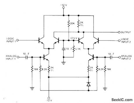
Circuit using Signetics 511 transistor array provides digital selection of either of two analog signals. When logic input at left is zero, signal at analog input 1 goes to output and other analog input signal is rejected. Similarly, when logic 0 is applied to logic input 2, analog input 2 goes to output. Eight-channel analog multiplex switch can be formed by combining four 511 analog switches with Signetics 8250 binary-to-octal decoder. Analog signals up to 200 kHz are switched without amplitude degradation.- Signetics Analog Data Manual, Signetics, Sunnyvale, CA, 1977, p 753-754. (View)
View full Circuit Diagram | Comments | Reading(0)
OVERLOAD_PROTECTION_FOR_REGULATED_POWER_SUPPLY
Published:2009/7/21 10:54:00 Author:Jessie
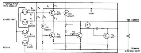
When rated load current is exceeded in series-regulated power supply, D1 conducts and collector voltage of Q1 acts as clamp to prevent further increase in load current. At short-circuit, load current is only fraction of full value.-K. L. Burfeindt, Over-load Protection Without High Power Dissipation, Electronics, 36:13, p 36-37. (View)
View full Circuit Diagram | Comments | Reading(807)
COMMUTATING_BANDPASS_FILTER
Published:2009/7/7 20:04:00 Author:May
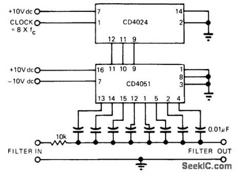
CD4051 analog multiplexer serves for commutation and switching of eight low-pass filter sections. Multiplexer is driven by CD4024 binary counter that is clocked at 8 times desired 100-kHz center frequency Can be tuned by varying commutating frequency.J Tracy, CMOS Offers New Aρproach to Commutating Filters. EDN Magazine, Feb,5,1974.ρ94-95.
(View)
View full Circuit Diagram | Comments | Reading(4420)
THYRATRON_PROTECTION_IN_HIGH_VOLTAGE_SWITCH
Published:2009/7/21 10:31:00 Author:Jessie
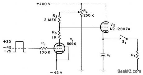
C1 is charged to some value up to 400 V, then discharged into load R5 by gas tube represented by S1. V2 acts as cathode follower to charge C1 as long as V1 does not conduct. When operation of S1 is desired, V2 is turned off by turning on V1 long enough for S1 to operate and recover, using square-wave input pulse. Circuit action prevents destruction of thyratron switch and load without sacrificing pulse rate. Tubes need separate filament transformers.-Voltage Controlled High Voltage Switch, Electronic Circuit Design Handbook, Mactier Pub. Corp., N.Y., 1965, p 233. (View)
View full Circuit Diagram | Comments | Reading(985)
1_kHz_COMB_FILTER
Published:2009/7/7 19:58:00 Author:May
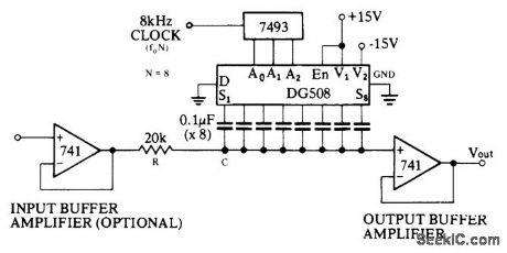
DG508 eight-channel CMOS multiplexer is used in comb filter having fundamental frequency of 1 kHz. Sampling action provides response at each harmonic multiple except at 8 and 16 kHz (no response at Nf0 or 2Nf0). Used in selective filtering of periodic signals from background of nonperiodic noise interference, 7493 TTL binary counter provides necessary 3-bit binary count sequence from 8-kHz clock. Q is 50.- Analog Switches and Their Applications, Siliconix, Santa Clara, CA, 1976, p 5-17-5-18. (View)
View full Circuit Diagram | Comments | Reading(2084)
BASIC_GTO_FOR_POWER_SUPPLY_OVERLOADS
Published:2009/7/21 10:30:00 Author:Jessie

Gate-turnoff scr (GTO) provides superior overload protection for d-c power supplies. Chief advantages are elimination of tum-on current surges, switching off within 30 microsec of overload, automatic load sensing, and reset, and no appreciable effect on power supply efficiency.-W. C. Mosley, GTO Protection Circuitry for DC Supplies, EEE, 12:11, p 57-59. (View)
View full Circuit Diagram | Comments | Reading(1234)
CONSTANT_BRIGHTNESS_CONTROL
Published:2009/7/7 9:59:00 Author:May

An automatic control maintains a lamp at a constant brightness over a wide range of supply voltages. This circuit utilizes the consistency of photodiode response to control the phase angle of power line voltage applied to the lamp and can vary the power between that available and ≈ 30% of available. This provides a candlepower range from 100% to less than 10% of nominal lamp output. The 100-μH choke, resistor, and capacitors form an rlc filter network that is used to eliminate conducted RFI. (View)
View full Circuit Diagram | Comments | Reading(869)
| Pages:978/2234 At 20961962963964965966967968969970971972973974975976977978979980Under 20 |
Circuit Categories
power supply circuit
Amplifier Circuit
Basic Circuit
LED and Light Circuit
Sensor Circuit
Signal Processing
Electrical Equipment Circuit
Control Circuit
Remote Control Circuit
A/D-D/A Converter Circuit
Audio Circuit
Measuring and Test Circuit
Communication Circuit
Computer-Related Circuit
555 Circuit
Automotive Circuit
Repairing Circuit