
Index 203
ELLIPTICAL_PAITERN
Published:2009/7/10 22:21:00 Author:May
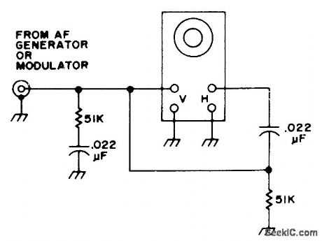
Connection shown gives Lissajous-type elliptical pattern on CRO from ordinary AF signal generator. Modulation can be added to eithervertical or horizontal feed for CRO.-Novice Q & A, 73 Magazine, March 1977, p 187. (View)
View full Circuit Diagram | Comments | Reading(622)
MICROPOWER_THERMOMETER
Published:2009/7/10 22:20:00 Author:May
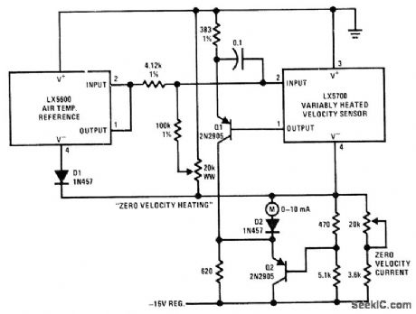
Low power consumption makes circuit attractive for battery-operated equipment. Uses National LX5600 temperature transducer covering -55℃ to +125℃, whose output is directly propor-tionalto absolutetemperature at l0 mV/K, Both zero and scale factor ale independently selectable. Thermometer is pulsed at low duty cycle to reduce power consumption, with sample and hold usedto obtain continuous output between pulses. Supply range is 8-12 V; 8.4-V mercury battery will give over 1 year of operational Iife. Output can be used to drive meter for direct readout. MVBR Q1-Q2 drives LX5600 through R9. C1 and R3 control OFF time, and C1, R1, R4, and R7 control ON time. Q3 issample transistor. Output is 0-50 μA for 50-100°F temperature change. Formulas in box give values for other ranges.-R. C. Dobkin, Micropower Thermometer, National Semiconductor, Santa Clara, CA, 1974, LB-27. (View)
View full Circuit Diagram | Comments | Reading(1285)
OPTOISOLATOR_FOR_PROBE
Published:2009/7/10 22:18:00 Author:May

Offsets need for potentially dangerous practice of floating oscilloscope with respect to ground. Also permits simultaneous display of two voltages with correct polarity on double-beam oscilloscope when one of them is floating. Texas Instruments TIL112 optocoupler used has bandwidth of about30 kHz, Three rangesgive choice of 1 :1, 10:1, and 100:1 input attenuation. Set RV2 to bias phototransistor of optocoupler to center of its linear range (about 4.5 V between pins 4 and 5), then set RV1 to give unity input/output ratio on range 1. RV3 is set to give zero DC output when input telminals are shorted, but can be omitted if zeroing of output level is unnecessary.-A. F. Sargent, Simple C.R.O. Input Isolating Probe, Wireless World, Feb. 1976, p 76. (View)
View full Circuit Diagram | Comments | Reading(1164)
5O0_W_VARIAB[E_PULSE_WIDTH_REGULATOR
Published:2009/7/10 22:16:00 Author:May
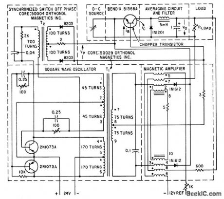
Chopper transistor supplies pulsewidth-modulated pulses to averaging circuit and filter. Filter output voltctge is compared to extemal reference voltage by magnetic am plifier, which changes pulse width to decrease devicttion. Chopper is driven by two-transistor square-wave oscillator modulated by mag-netic amplifier.-P. Bahhasctr, New Iransistor Regukttor Handles 500-Watt Outputs, Elec-tronics, 35:38, p48-49. (View)
View full Circuit Diagram | Comments | Reading(513)
HEXADECIMAL_ENTRY
Published:2009/7/10 22:15:00 Author:May
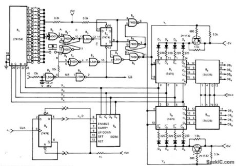
Permits entering program into microprocessor in hexadecimal notation, in much less time than is required with binary notation. Binary switches from input port of μP are replaced with 16-key keyboard shown. To enter hexadecimal number 3B, turn on power; press 3 button, press decimal bar, then press B button; operate loading switch, then press decimal bar again to set keyboard for next entry. Article traces keyboard operation through circuit.-B. K. Erickson, Talk to Your μP with a Hex-Latching Keyboard, EDN Magazine, Nov. 20, 1976, p 319-320. (View)
View full Circuit Diagram | Comments | Reading(2000)
SIMPLE_RIPPLE_SUPPRESSOR
Published:2009/7/10 22:15:00 Author:May
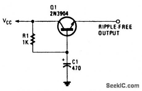
This circuit, at times called a capacitance multiplier, is useful for suppressing power-supply ripple. C1 provides filtering equal to a capacitor of (B+1) C1, where B=dc current gain of Q1 (typically > 50). (View)
View full Circuit Diagram | Comments | Reading(0)
REGULATED_CHARGE_PUMP
Published:2009/7/10 22:13:00 Author:May
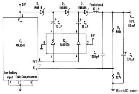
The dc-dc converter substitutes a voltage tripler in place of the external inductor and the diode that's typically associated with the switching regulator, IC1. Inverting and noninverting amplifiers in the MOS-FET-driver (IC2) activate a diode-capacitor tripling network (D1 through D3, C1 through C3).A 50-kHz oscillator residing within IC1 produces the EXT signal (pin 6). IC2 converts this signal into drive signals (180°out of phase) for the tripler. The resulting charge-discharge action in the capacitors recharges C3 toward 10 V every 20 μs. The ferrite bead limits output ripple to about 20-m Vpp for a 50-mA load. Conversion efficiency is about 70% for the 5-V input, 10-V output configuration. (View)
View full Circuit Diagram | Comments | Reading(778)
LOW_POWER_TOUCH_TONE_DECODER
Published:2009/7/10 22:11:00 Author:May
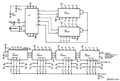
This decoder will respond to a preselected 4-digit DTMF number. IC7 is a Radio Shack IC device (part #276-1303). The logic is all CMOS. The digits are selected by SW1 and SW2, a pair of 8-position DIP switches. (View)
View full Circuit Diagram | Comments | Reading(1956)
SCANNING_ASCI_NECODER
Published:2009/7/10 22:10:00 Author:May
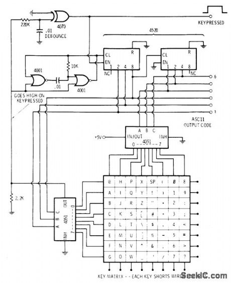
Converts key action into composite parallel ASCLL code. Circuit includes debouncing and two-key rollover. Two 4001 quad two-input NOR gate sections form 50-kHz clock that is gated. When clock is allowed to run, two cascaded 4520 binary counters are driven for continuous cycling through all their counts. Slower counter pro-duces 1-of-8 decoded output for 4051 1-of-8 switch. Faster counter drives second switch that monitors sequential rows of characters.When key is pressed, output from +5Vthrough both selectors stops gated oscillator and holds count. Resulting ASCll output is then routed to external output logic for control and shift operations. When key is released, scanning resumes and continues until new key is pressed.If second key is pressed before first is released, nothing happens until first key is released.Scanning then resumes and stops at second key location, to give two-key rollover permitting faster typing with minimum error.-D. Lancaster, CMOS Cookbook, Howard W. Sams, Indianapolis, IN, 1977, p 358-359. (View)
View full Circuit Diagram | Comments | Reading(779)
V_F_AND_F_V_CONVERTERS_FOR_DPM
Published:2009/7/10 22:08:00 Author:May
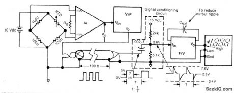
Signaltransmitted as variations in frequency in 0-10kHz range is conerted back to voltage for driving digital panel meterto give indication of temperature value sensed by 100-ohm resistive thermal device (RTD) in bridge V/Fand F/V converters can be almost any commercial modelsdes gned for 0-10 V and 0-10 kHz,Instrument amplifier can be Datel AM201 or equivalent.-E.L.Murphy,Sending Transducer Signals over 100 Feet?, lnstruments & Control Systems,June 1976, p35-39. (View)
View full Circuit Diagram | Comments | Reading(607)
12_V_INPUT_SIMPLE_INVERTER
Published:2009/7/10 22:05:00 Author:May
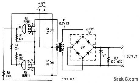
Using two power MOSFETs, this inverter can deliver ac or dc up to several hundred volts. T1 is a 12.6-V CT to 120-, 240-, or 480-V transformer for 60-Hz application. (View)
View full Circuit Diagram | Comments | Reading(1879)
DUPLEX_AUDIO_LINK
Published:2009/7/10 22:05:00 Author:May
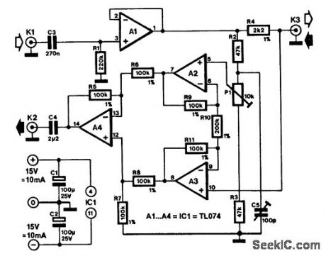
Duplex communication is, of course, not a new technique: it has been used, for instance, in telephone systems for many years. Those systems, however, use transformers to achieve duplex-this circuit does it with the aid of electronics.The principle is fairly simple. Two senders impose signals (U1 and U2, respectively) on to the audio cable. The voltage across the cable is then (U1+ U2)/2. The receivers at both sides of the cable deduct their side's sender signal from the cable signal: the result is that the signal is sent from the other end of the cable. This principle is the basis of the circuit shown. Notice that a similar circuit is required at either end of the link.Op amp A1 is connected as a buffer amplifier and serves as sender. The send signal is imposed on the cable via R4. Terminating the cable by R4 results in the voltage across the cable being only half the voltage output of A1. This does not detract from the operation of the circuit, however. At the same time, R4 ensures that signals emanating from the other end of the link cannot get to the output of A1; if they could, they would be short-cii-cuited by the output.The receiver is a differential amplifier consisting of op amps A2 through A4. The quality of the differential amplifier depends largely on the resistors used with the op amps; 1% types are, therefore, essential.The cable signal, (U1+ U2)/2, is applied to one input of the differential amplifier and the (halved) output signal of A1 to the other. Because the differential amplifier has a gain of 6 dB, the received signal applied to K2 has the same level as the original signal.The circuit is calibrated by connecting the cable to it and to its twin circuit, then injecting a 1-kHz sinusoidal signal and a 5-Vrms level to its input. The input bus of the other circuit must be short-circuited during the calibration. Adjust P2 for minimum signal at K2. Next, increase the frequency of the input signal to 10 kHz and adjust C5 for a minimum signal at K2. Repeat the procedure with the other circuit. The signal suppression at 1 kHz is of the order of 80 dB; at 20 kHz, it is approximately 60 dB.
(View)
View full Circuit Diagram | Comments | Reading(896)
ELECTRONIC_TELETYPE_KEYBOARD
Published:2009/7/10 22:04:00 Author:May
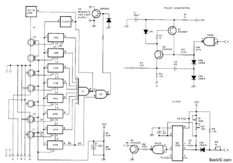
Uses eight 7474 shift register sections in combination with pulse generator that is discharged through appropriate toroid core to create correct markspace coding for energizing magnet drivers of Teletype. Developed to permit communication by handicapped people. Simplified keyboard has one set of alphabetic characters and five numeries for BCD input, Outputs of shift registers drive 7430 NAND gate U2. If keyboard is to be used at 60 WPM, adjustR1 so 555 oscillates at 45 Hz. Toroids are Indiana General CF.102 having 10-turn primaries.-L. A Stapp, Electronie Teleprinter Keyboard, Ham Radio, Aug.1978, p 56-57.
(View)
View full Circuit Diagram | Comments | Reading(1335)
CURSOR_FOR_TV_TYPEWRITER
Published:2009/7/10 22:04:00 Author:May
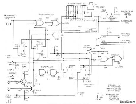
Complete CMOS logic cursorand update system is shownfor system using RAM memory,direct memory access, and writing during vertical intenral for displaying 512 characters per page on TV screen, Extemal 7.5-Hz source is required to make undedine cursorflash to indicate position at which next character will be entered on screen.-D, Lancaster, TV Typewriter Cookbook, Howard W .Sams,Indianapoils,IN,1976,p 128-129 (View)
View full Circuit Diagram | Comments | Reading(647)
FOUR_CHANNEL_ADAPTER_FOR_CRO
Published:2009/7/10 22:00:00 Author:May
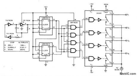
DG201 CMOS analog switch controlled by 50-kHz clock allows display of four input signals simultane-ously on singletrace oscilloscope, Adapter is used in chop mode for signals below 500 Hz. Frequencies above 500 Hz are best viewed in altemate mode with clock frequency of 200 Hz. One of inputs is used to trigger horizontal trace of CRO.- Analog Switches and Their Applications, Siliconix,Santa Clara,CA,1976,p7-63-7-66. (View)
View full Circuit Diagram | Comments | Reading(909)
LOW_Z_INPUT
Published:2009/7/10 21:59:00 Author:May
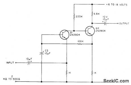
Can be used with low-impedance source, such as 4- to 16-ohm loudspeaker or telephone earphone used as mike. If loudspeaker is put out in yard, sensitivity is sufficient to pick up sounds made by prowlers. Can.be fed into input of any high-fidelity amplifier.-E. Dusina, Build a General Purpose Preamp, 73 Magazine, Nov. 1977, p 98.
(View)
View full Circuit Diagram | Comments | Reading(744)
±7_VDC_OFFSET
Published:2009/7/10 21:58:00 Author:May
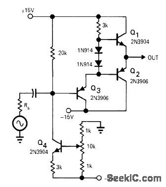
High-impedance current source Q4 provides desired level shiftfor AC signals in video circuit whose DC level controls intensity of CRT. Input and offset signals are fed to base of Q3 which drives complementary-symmetry emitter-follower Q1-Q2. For values shown, level can be shifted about ±7 VOC.-P.B. Uhlenhopp, Variable DC Offset Using a Current Source, EDN|EEE Magazine, Aug. 15, 1971, p46. (View)
View full Circuit Diagram | Comments | Reading(802)
CATHODE_DRIVE_FOR_CRT
Published:2009/7/10 21:57:00 Author:May
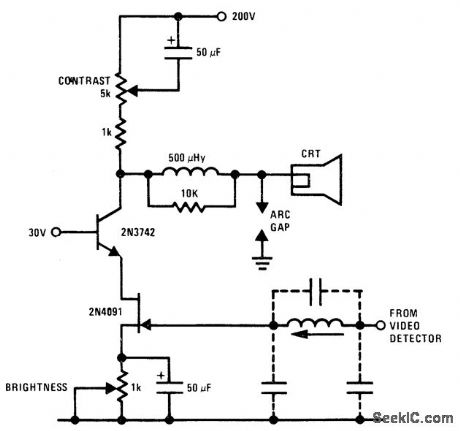
Cascode connection of 2N4091 JFET and 2N3742 bipolar transistor provide full video output for cathode. Gain is about 90. M-derived filter using stray capacitances and variable inductor blocks 4.5-MHz sound frequency from video amplifier. Cascode coAfiguration eliminates Miller capacitance problems of JFET, allowing direct drive from video detector.- FET Databook, Na-tional Semiconductor, Santa Clara, CA, 1977, p 6-26-6-36. (View)
View full Circuit Diagram | Comments | Reading(1049)
COMMUTATOR
Published:2009/7/10 21:57:00 Author:May
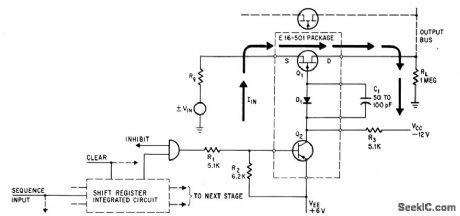
Bipolar pnp trcmsistor, diode, and fet lransislor in basic module form analog switch used as electronic commutator for choppers and telemetry multiplexing.-J, Gulbenk and T. F. Prosser, How Modules Make i Complex Design Simple, Electronics,37:32, p50-54. (View)
View full Circuit Diagram | Comments | Reading(1509)
HIGH_GAIN_INTERCOM
Published:2009/7/10 21:54:00 Author:May
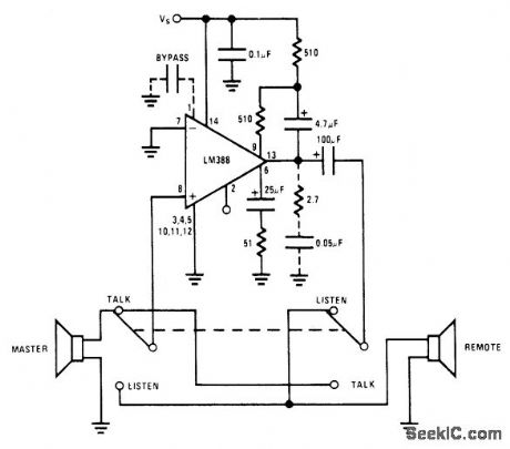
Internal bootstrapping in National LM388 audio power amplifier IC gives output power levels above 1 W at supply voltages in range of 6-12 V, with minimum parts count. AC gain is set at about 300 V/ V, eliminating need for stepup transformer nor mally used in intercoms. Optional RC network suppresses spurious oscillations.- Audip Handbook, National Semiconductor, Santa Clara, CA, 1977, p 4-37-4-41. (View)
View full Circuit Diagram | Comments | Reading(817)
| Pages:203/471 At 20201202203204205206207208209210211212213214215216217218219220Under 20 |
Circuit Categories
power supply circuit
Amplifier Circuit
Basic Circuit
LED and Light Circuit
Sensor Circuit
Signal Processing
Electrical Equipment Circuit
Control Circuit
Remote Control Circuit
A/D-D/A Converter Circuit
Audio Circuit
Measuring and Test Circuit
Communication Circuit
Computer-Related Circuit
555 Circuit
Automotive Circuit
Repairing Circuit