
Index 214
OPTICAL_RECEIVER
Published:2009/7/10 1:54:00 Author:May
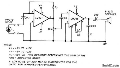
An optical receiver for light-wave communications, this circuit works with AM-type light signals. (View)
View full Circuit Diagram | Comments | Reading(3383)
dc_dc_CONVERTER
Published:2009/7/10 1:53:00 Author:May
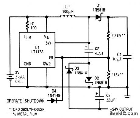
This circuit uses a Linear Technology LT1073 in a -24-V converter. The supply can be two AA cells (3 V) or 5 V. The circuit can deliver 7 mA. (View)
View full Circuit Diagram | Comments | Reading(3515)
6_W_WARBLE_TONE_SIREN
Published:2009/7/10 1:53:00 Author:May

This circuit uses a CMOS chip and a VMOS FET amplifier for 6 W of audio output. 18 W of audio canbe generated usmg a+24-Vdc supply, IC1A and IC1B are used as a 1-Hz oscillator. IC1C and IC1D form a 1-kHz multivibrator that is gated by the 1-Hz signal from IC1A and IC1B. (View)
View full Circuit Diagram | Comments | Reading(1384)
ELECTRONIC_SIREN
Published:2009/7/10 1:52:00 Author:May
The wailing sound of a siren is generated by a VFO consisting of Q1 and Q2. Capacitor C2 provides the feedback for the oscillator. The frequency of the oscillator is varied by the voltage applied to the base of Q1 hrough R3 .When switch S1 is closed, capacitor C1 charges, thus increasing the oscillator frequency.When S1 is released, capacitor C1 discharges, and the oscillator frequency decreases. Capacitor C3 limits the maximum oscillator frequency. The average battery current drain is about 15 mA. (View)
View full Circuit Diagram | Comments | Reading(2582)
WIDEBAND_FET
Published:2009/7/10 1:51:00 Author:May
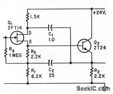
Feedback and bootstrapping techniques give overall input capacitance of 0.4 pf for 30-pf gate capacitance of fet.Transislor serves as source follower.-B. Down, Using Feedback in FET Circuit to Reduce Input Capacitance, Electronics, 37:31, p 63-65. (View)
View full Circuit Diagram | Comments | Reading(842)
μP_CONTROLLED_NEGATIVE_VOLTAGE_CONVERTER
Published:2009/7/10 1:49:00 Author:May
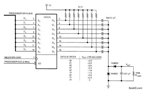
This circuit was used to produce a variable negative voltage for contrast control of an LCD display. A 74F374 generates a square wa:ze that is ac coupled to a rectifter and load. By using the μP clock and data from the processor bus, and properly timed load signal, the dc level generated can be controlled by the μP. (View)
View full Circuit Diagram | Comments | Reading(526)
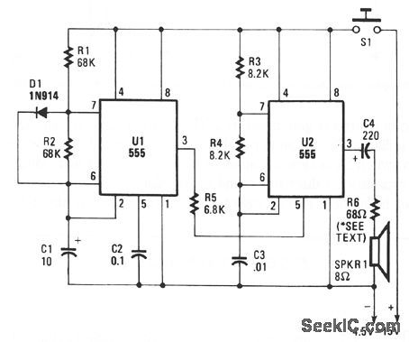
ALTERNATE_WARBLE_TONE_SIREN
Published:2009/7/10 1:49:00 Author:May
This circuit uses two NE555 timers to generate a warble tone. IC1 frequency shifts IC2 by feeding a square waxe to pin 5, the modulation input of IC2. IC1 runs at about 1 Hz (View)
View full Circuit Diagram | Comments | Reading(826)
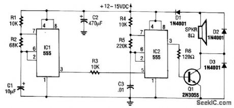
HEE_HAW_SIREN
Published:2009/7/10 1:48:00 Author:May
A pair of timer IC's are the heart of a circuit that simulates the warbling hee-haw of a British police siren. One of the 555 timers, U2, is wired as an astable multivibrator operating at about 900 Hz. The other, U1, operates at approximately 1 Hz. Its output at pin 3 is a square wave with a 50% duty cycle-on and off cycles of about 0.5 second each. The output of U1 is applied to pin 5, the control-voltage terminal of U2. The frequency of the 555 timer IC is relatively independent of supply voltage, but can be varied ever a fairly wide range by applying a variable voltage between pin 5 and ground. When U1's output becomes high, U2 operates at about 800 kHz. That switching between two frequencies produces the warbling hee-haw signal. (View)
View full Circuit Diagram | Comments | Reading(2906)
LINEAR_IC_SIREN
Published:2009/7/10 1:45:00 Author:May


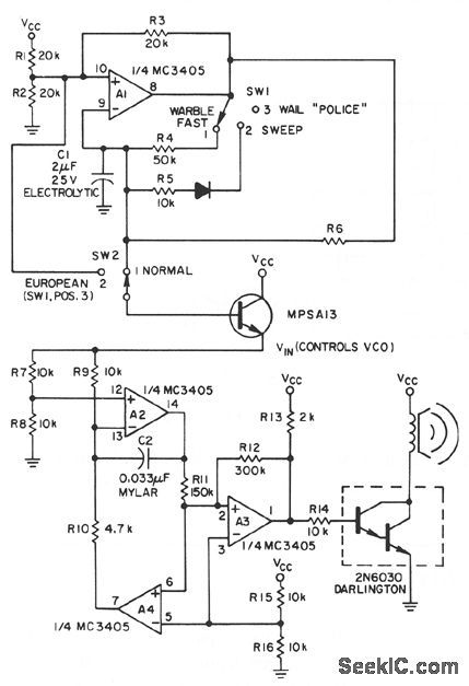
A low-frequency, op-amp oscillator and a VCO, both configured from a single MC3405 dual op amp and dual comparator, are the major components in a siren circuit that can be made to produce various warbles and wails, or serve as an audio sweep generator. The only other active components needed are an MPS A13 small-signal transistor and a 2N6030 power Darlington transistor. (View)
View full Circuit Diagram | Comments | Reading(689)
RECTANGULAR_TRIANGULAR_WAVEFORM_CONVERTER
Published:2009/7/10 1:44:00 Author:May
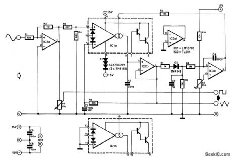
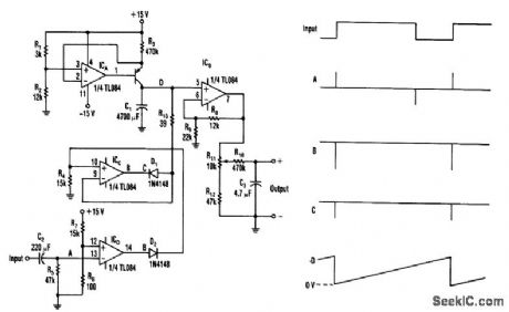
Many function generators are based on a rectangular waveform generator that consists or a Schmitt trigger and integrator. The triangular signal produced by the integrator is then used to form a sinusoidal signal with the aid of a diode network. The converter presented here works the other way around. It con-verts the output of a good-quality sine-wave oscillator into a rectangular and a triangular siant.
The sinusoidal siinal is converted into a rectangular signal by IC2A. Because the output of this gate varies between - 15 V and + 15 V, it is reduced to a value that is suitable for integration by potential divider R3/R4. It is then integrated by transconductance amplifier IC1A and C2. The amplifier has a current output that is controlled by the current through pin 1. The output therefore behaves as a resistance, with which it is possible to influence the integration time.
The voltage across C2 is available in buffered form at the output of impedance inverter IC2B; this is the triangular signal. The amplitude of this signal is compared with a voltage set by P2 and the difference between these voltages, which is the output of IC2C, is applied to the current source at the output of IC1 via R5. This arrangement ensures that the level of the output voltage is virtually independent of the frequency of the rectangular signal or of the sinusoidal input.
One problem with a precision integration is its being affected by offset voltages and bias currents. Feedback loop R6/C1 ensures that the output follows the potential across R4 accurately. However, tiny deviations might be caused by the bias current in circuit IC1, which is not greater than 8 μA at 70℃.The time constant R6/C1 is large for a purpose: to ensure that the triangular signal, even at low fre-quencies, cannot affect the waveform of the signal to be integrated-the rectangular shape must be retained. The converter can process signals at frequencies from 6 Hz (where the amplitude is not affected) to 60 kHz (where the amplitude is reached by 10%).
Because of the long time constants, the time taken for the recovery of the amplitude of the triangular signal at frequencies above 1 kHz is rather long. The peak value of this signal should be set to 1 V.
Diode D1 is a so-called sfaGa'slot-three diodes in one package. It might be replaced by three discrete type 1N4148 diodes. The current drawn by the converter is of the order of 9 mA.
(View)
View full Circuit Diagram | Comments | Reading(1579)
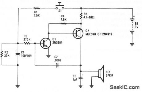
THE_WAILING_SIREN
Published:2009/7/10 1:44:00 Author:May
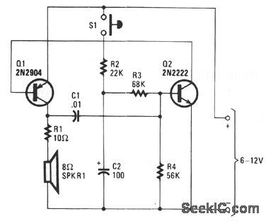
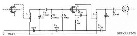
Transistors Q1 and Q2, with feedback provided via C1 from the collector of Q1 to the base of Q2, forms a voltage-controlled oscillator (VCO). Depending on the voltage applied to Q2's base, the VCO frequency ranges from around 60 Hz to 7.5 kHz. The instantaneous voltage applied to the base of Q2 is determined by the values of C2, R2, R3, and R4. When pushbutton switch S1 is closed, C2 charges fairly rapidly to the maximum supply voltage through R2, a 22-KΩ fixed resistor. That causes the siren sound to rise rapidly to its highest frequency. When the button is released, the capacitor discharges through R3 and R4 with a combined resistance of 124 KΩ, causing the siren sound to decay from a high-pitched wail to a low growl. If you want to experiment with the pitch of the sound at its highest frequency, try different values for C1. ncrease its value for lower notes, and decrease it for higher ones. Different values for R2 will change the attack time. A 100-KΩ resistor provides equal attack and decay times. The way you handle the pushbutton varies the effect. (View)
View full Circuit Diagram | Comments | Reading(1034)
PROGRAMMABLE_FREQUENCY_ADJUSTABLE_RATE_SIREN
Published:2009/7/10 1:42:00 Author:May
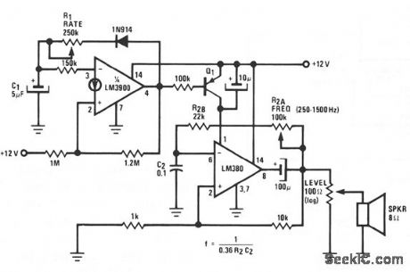
The LM380 operates as an astable oscillator with the frequency determined by R2/C2. Adding Q1 and driving its base, with the output of an LM3900 wired as a second astable oscillator, acts to gate the output of the LM380 on and off, at a rate fixed by R1/C1. (View)
View full Circuit Diagram | Comments | Reading(908)
YELPING_SIREN
Published:2009/7/10 1:41:00 Author:May
Unijunction transistors Q1 and Q2 are both connected as relaxation-type, sawtooth oscillators. Transistor Q1 is the low-frequency control oscillator and Q2 is the tone generator. Sawtooth waveforms are produced at the emitter terminals. Without R4 connecting the two emitters, each oscillator operates inde-pendently, with its frequency determined mainly by the re time constant. With the values shown, Q1 operates from 1. to 1.5 Hz and Q2 operates from 400 to 500 Hz. When R4 is connected between the two emitters, it couples the low-frequency sawtooth from Q1 directly across capacitor C2. That coupling causes the frequency of the tone generator to increase, along with the rise in sawtooth voltage from Q1.The tone generator's frequency drops to its lower design value when C1 discharges and produces the fall-ing edge of the sawtooth. (View)
View full Circuit Diagram | Comments | Reading(2283)
UNNEUTRAIZED_MOS_FET
Published:2009/7/10 1:40:00 Author:May
Low draim-gate capacitance is needed for high power gains above 2 Mc from common-source mos fet.-G.G.Luettgenau and S. H. Barnes, Designing With Low-Noise MOS FETs: A Little Different But No Harder, Electronics, 37:31, p 53-58. (View)
View full Circuit Diagram | Comments | Reading(512)
GEIGER_COUNTER
Published:2009/7/20 0:45:00 Author:Jessie
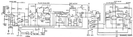
Simple basic monitor provides continuous audio end visual indications of radioactive materials in industrial areas. If recording is required, four leads at right are connected to 10-cps keep-alive mvbr and triode output stage for driving recorder. Will handle count rates up to 10,000 per minute. Strobotron V3 in pulse equalizer provides visual indications.-R. L. Ives, Geiger Radiation Monitor Indicates Continuously, Electronics, 31:43, p 93-95. (View)
View full Circuit Diagram | Comments | Reading(0)
HEE_HAW_ELECTRONIC_SIREN
Published:2009/7/10 1:40:00 Author:May
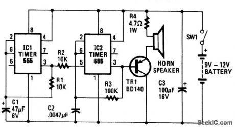
The oscillator based on IC2 is responsible for producing the sound. Its output is connected to the base of TR1, which amplifies it to drive the speaker. Resistor R4 is included in the circuit to limit the current through TR1 to a safe and reasonable level. The oscillation frequency of IC2 is partially dependent on the values of R3 and C2. Another factor that governs the frequency of oscillation is the magnitude of voltage fed to pin 5 of IC2. If a voltage of varying magnitude is fed to pin 5, the internal circuitry of the IC is forced to reset at a different rate, which changes the frequency.IC1 is also connected as an oscillator,but it runs much slower than IC2: around 1 Hz. Each time the IC triggers, the voltage at pin 3 goes high. As pin 3 is connected to pin 5 of IC2, this forces IC2 to change its note. That produces the hee-haw sound of the siren. (View)
View full Circuit Diagram | Comments | Reading(1022)
PERIOD_TO_VOLTAGE_CONVERTER
Published:2009/7/10 1:39:00 Author:May
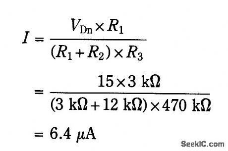
ICA,R1, R2, R3, and Q1 form a current source. The current that charges C1 is given by:
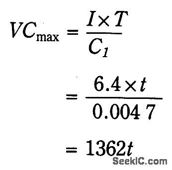
The input signal drives ICD. Because ICD's positiveinp ut (V+)is slightly offset to +0.1V, its steady state output will be around + 13 V. This voltage is sent to ICC through D2, setting ICC's output to + 13 V.Therefore, point D is cut off by D1, and C1 is charged by the current source. Assuming the initial voltage on C1 is zero, the maximum voltage (VCmax) is given by:
If f=1 ms, then VCmax = 362 V.
When the input goes from low to high, a narrow positive pulse is generated at point A. This pulse becomes - 13 V at point B, which cuts off D2. ICC's V+ voltage becomes zero. The charge on C1 will be absorbed by ICC on in a short time. The time constant of C2 and R5 determines the discharge period-about 10 ps. ICB is a buffer whose gain is equal to (R8+R9)÷R9-1.545. ICD's average votiage will be (1362fx1.545)÷2=1052t. R10 and C3 smooth the sawtooth waveform to a dc output. (View)
View full Circuit Diagram | Comments | Reading(792)
TWO_TONE_SIREN
Published:2009/7/10 1:39:00 Author:May

This siren provides a constant audio output, but alternates between two separate tones. The LM13080 is set to oscillate at one basic frequency; this frequency is changed by adding a 200-KΩ charging resistor in parallel with the feedback resistor, R2. (View)
View full Circuit Diagram | Comments | Reading(1434)
RESPONSE_BELOW_2_CPS
Published:2009/7/10 1:39:00 Author:May
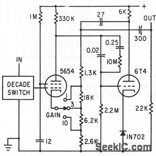
With input resistance of 1,000 meg,piezoelectric gage amplifier gives gain choices of 1,3,or 10 for loads above 2,500 ohms.Decade input swith can provede choice of shunt capacitances for trimming sensitivety of gages.-Extending Piezoeldtric Gage L-F Response,Electronics,36:4,p 100-103. (View)
View full Circuit Diagram | Comments | Reading(561)
ELECTRONIC_BAGPIPE
Published:2009/7/10 1:38:00 Author:May


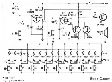
This circuit mimics the dual-tone drone sound that's produced by the unusual wind instrument. Unijunction transistors Q1 and Q2 are connected in similar audio-oscillator circuits. Each of the oscillator frequencies is determined by one of the two resistors selected by one of the pushbutton switches, S4 through S11. The odd-numbered resistors in R7 to R21, determine the frequency for the Q1 oscillator circuit and the even-numbered resistors in R8 through R22, determine the frequency for Q2's circuit.When S4 is pressed, the positive supply is connected to both R7 and R8 through isolation diodes D1 and D2, causing both oscillators to operate. A narrow, fast-rising positive pulse is developed at B1 of both Q1 and Q2 for each cycle of operation. Transistors Q3 and Q4 serve as a simple audio mixer, which is used to combine the pulses from each oscillator. The mixed signal at the collectors of Q3 and Q4 is coupled through R6 to the base of Q5, which amplifies and drives an 8-Ω speaker, SPKR1. Switches, S2 and S3 are used to reduce the oscillator's frequency by about 50% when closed, to produce a new group of tones. (View)
View full Circuit Diagram | Comments | Reading(2202)
| Pages:214/471 At 20201202203204205206207208209210211212213214215216217218219220Under 20 |
Circuit Categories
power supply circuit
Amplifier Circuit
Basic Circuit
LED and Light Circuit
Sensor Circuit
Signal Processing
Electrical Equipment Circuit
Control Circuit
Remote Control Circuit
A/D-D/A Converter Circuit
Audio Circuit
Measuring and Test Circuit
Communication Circuit
Computer-Related Circuit
555 Circuit
Automotive Circuit
Repairing Circuit