
Index 202
PHONE_IN_USE_INDICATOR
Published:2009/7/10 23:08:00 Author:May
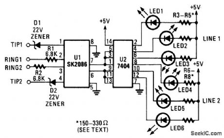
The circuit receives its power from a 15-V wall adapter (not shown). The circuit takes advantage of the fact that the phone line voltage drops from 48 to 10 V when an extension is taken off the hook. When the voltage on a line drops, the optoisolator/coupler is turned off so that the inputs to the line-1 hexinverters (U2 pins 1. 3. and 5) float high. The corresponding outputs (U2 pins 2. 4. and 6) go low and light the line-1 LEDs. (View)
View full Circuit Diagram | Comments | Reading(1092)
NORMALLY_OFF_GTO_CHOPPER
Published:2009/7/10 23:01:00 Author:May
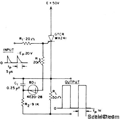
Small trigger at input generates high.power pulse with duration determined by time constant R2-C1.Gate-turnoff controlled recliner in this circuit will chop 1 kw at 1 kc.-J.W. Motto, Jr, Switching Circuits Using the Gate Turnoff Controlled Rectifier, EEE, 11:3, p52-55. (View)
View full Circuit Diagram | Comments | Reading(511)
SERVOED_SHIELD_FOR_PROBE
Published:2009/7/10 22:59:00 Author:May
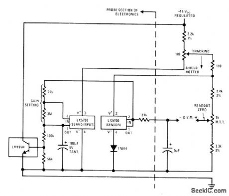
Used when only part of temperature sensor can touch surface being measured. LM195H powertransistor is main power amplifier and at same time serves as 23-W heater that is used to make copper shield track actual temperature of surface to be measured. Uses National LX5700 sensors. Diode in series with ground leg of one sensor permits adjusting pin 3 of that sensor over range of 40-80 mV to make it track with servo thermometer. Digital voltmeter is used to read temperature directly in degrees C.-P. Lefferts, A New Interfacing Concept; the Monolithic Temperature Transducer, National Semiconductor, Santa Clara, CA, 1975, AN-132, p 6. (View)
View full Circuit Diagram | Comments | Reading(555)
VARIABLE_WIDTH_AND_PRF
Published:2009/7/10 22:59:00 Author:May
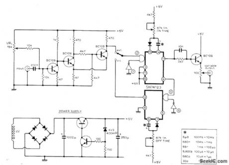
Low-cost pulse generator uses versatile dual monostable IC to provide clock pulses that gan be varied in width over wide range bv changing sizes of two extemal capacitors and adiusting 47K linear pots.Switched bank of six capacitors can be used instead, to give on or off times ranging between 100 ms and 100 ns, asgiven in table. With switch in external position, on-time mono is driven by three transistors connected as Schmitt trigger giving pulse having same trequency as that of input signal. VR1 sets trigger level. Suitable regulated 5-V supply circuit is also shown,-J. Garrett, Pulse Generator, Wireless Workl, Feb.1976,p78. (View)
View full Circuit Diagram | Comments | Reading(602)
VOLTAGE_REFERENCE_TH_ERMOM_ETER
Published:2009/7/10 22:58:00 Author:May
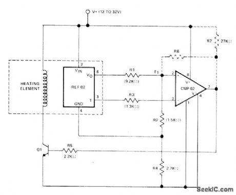
Pre-cision Monolithics comparator CMP-02 tums on heating-element driver Q1 when temperature drops below set point determined by ratio of R1 to R2, as sensed by +5 V voltage reference REF02 serving as thermometer. Circuit also provides adjustable hysteresis, determined by R6 and R7, if this feature is desired. Values in parentheses are for 60℃ set point. REF-02 should be thermally connected to substance being heated. Design equations are given.- Linear & Conversion I.C. Products, Precision Monolithics, Santa Clara, CA, 1977-1978, p 15-4. (View)
View full Circuit Diagram | Comments | Reading(964)
GLITCH_CORRECTOR
Published:2009/7/10 22:58:00 Author:May
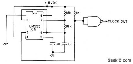
Circuit shown prevents TTL devices from seeing two clock pulses when output of 555 timer has glitch on falling edge atabout 0.8 V.-J Magee,Glitch,73 Magazine, Jan 1976, p10. (View)
View full Circuit Diagram | Comments | Reading(616)
CENTERING_CLOCK_SIGNAL
Published:2009/7/10 22:58:00 Author:May
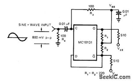
Circuit generates DC bias across complementarv outputs of Motorola MC10131 flip-flop for optimum operation with emitter-coupled logic (10,000 series).Bias is independent of state of flip-flop, which uses toggle frequency of about 150 MHz. Article covers applications for other flip-flops and counters requiring maintenance of best toggle frequency over wide temperature range.-T.Balph and H. Gnauden, Build a Clock Bias Circuit for ECL Flip-Flops, EDN fllagazine, May 5, 1976, (View)
View full Circuit Diagram | Comments | Reading(1103)
PRINTED_CIRCUIT_CHOPPER
Published:2009/7/10 22:54:00 Author:May
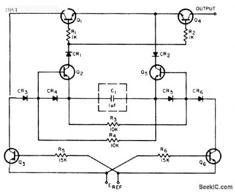
Uses convenlional Bright chopper connected to reference supply through coupler, constructed on ceramic chip. Q1 and Q4 are 2N914 matched pairs, Q2 and Q3 ore 2N2412, and Q5 and Q6 are 2N914. All diodes are IN914.-D.D. Robinson, Application of Integrated Circuits: An Evolutionary Approach, EEE, 12:4, p 42-47. (View)
View full Circuit Diagram | Comments | Reading(533)
SAUARE_WAVE_CLOCK
Published:2009/7/10 22:51:00 Author:May
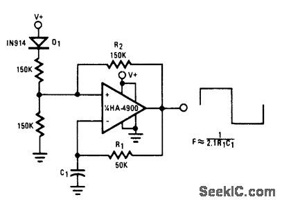
One section of Harris HA-4900/4905 precision quad comparator gives excellent frequency stability as self-starting fixed-frequency square-wave generator for clock applications, R1 and C1 determine frequency, and R2 provides regenerative feedback.For higher precision at frequencies up to 100 kHz, crystal may be used in place of C1.- Linear & Data Acquisition Products, Harris Semiconductor, Melbourne, FL, Vol. 1, 1977, p 2-96. (View)
View full Circuit Diagram | Comments | Reading(512)
ANSWERING_MACHINE_BEEPER
Published:2009/7/10 22:51:00 Author:May
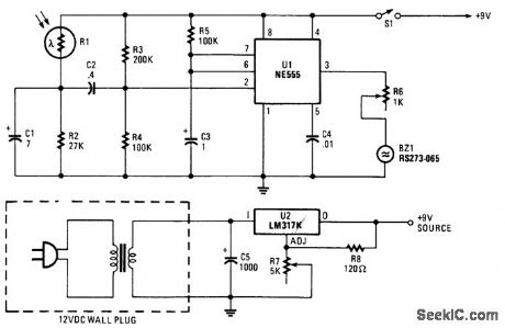
When the light on the answering machine blinks, the resistance of photoresistor R1 charges, triggers the timer (U1), and generates 0.2-s pulse that activates BZ1. R1 is optically coupled to the LED on the answering machine and is properly light shielded. (View)
View full Circuit Diagram | Comments | Reading(570)
TWO_PHASE_CLOCK_TO_1_MHz
Published:2009/7/10 22:51:00 Author:May
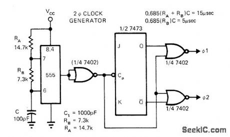
Signetics 555 timer is used as oscillator to generate nonover-lapping clock pulses as required for most two-phase dynamic MOS memories and shift registers. Duty cycle is determined by values of extemal resistors RA and RB which, together with timing capacitor C, determine frequency of os cillation. 7473 flip-flop controls phase that is switched on through 7402 NOR gates. Article gives timing waveforms and equations. Maximum operating frequency is 1 MHz.-G. Schlitt, Monolithic Timer Generates 2-Phase Clock Pulses, EDNMagazine, Aug. 1, 1972, p 57. (View)
View full Circuit Diagram | Comments | Reading(747)
FOUR_PULSE_BURST
Published:2009/7/10 22:45:00 Author:May
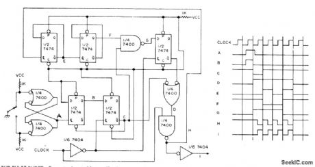
Generates burst of four clock pulses each time switch is pressed, Modifications ean produce any desired number of pulses in burst. Reliability of pulse count is ensured by use of debouncing latch using pair of 7400 gates,VCC is +5V,-E.E.Hrivnak,House Cleaning the Logical Way,73 Magazine, Aug.1974,p 85-90. (View)
View full Circuit Diagram | Comments | Reading(660)
PHOTOCONDUCTIVE_CHOPPER
Published:2009/7/10 22:42:00 Author:May
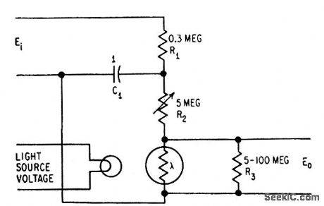
Combines low noise level With resistance to vibration.R1 prevemls bumup of photocell,R2 glves maximum conversion efficency at setting of about 2.2 meg.C1 averages d-c input signal fluctuations so they do not exceed 120-cps chopping frequency of light source.-R.G. Seed,Chopper Uses New Photocells,Electronics,31:21,p90-98. (View)
View full Circuit Diagram | Comments | Reading(460)
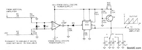
TRIGGERED_SWEEP_FOR_CRO
Published:2009/7/10 22:40:00 Author:May
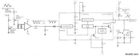
Combination of 555 timer and standard opamp minimizes cost of adding triggered sweep to oscilloscope not having this feature. Timer is triggered by applying vertical-amplifier signal through opamp, initiating charging of sweep capacitor C. When capacitor voltage reaches control voltage of timer (0.33 VCC), flip-flop in timer resets and capacitor discharges to form retrace of sweep.- Signetics Analog Data Manual, Signetics, Sunnyvale, CA, 1977, p 726. (View)
View full Circuit Diagram | Comments | Reading(1596)
CALCULATOR_KEYBOARD_INPUT
Published:2009/7/10 22:36:00 Author:May
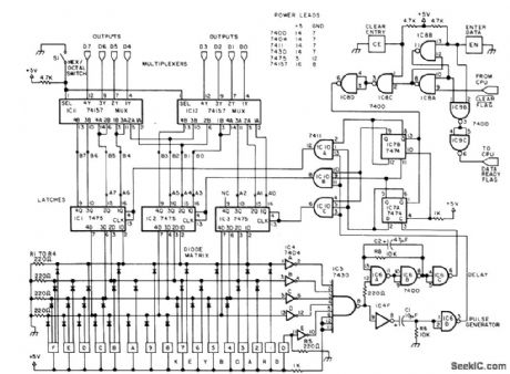
Uses diode matrix that encodes 16 hexadecimal input keys as 4-bit code for microprocessor. Register holds conversion results. Multiplexer gives switch-selected 3-digit octal or 2-digit hexadecimal interpretation to inputs. Control logic serves for keyboard debouncing, cleafing, and entering data.Circuit eliminates need for entering programs with front-panel switches, by using keyboard to enter data in octal or hexadecimal form. Choice of form is achieved with 74157 multiplexors IC11 and IC12, set by S1. Article covers circuit operation in detail and gives 8008 full keyboard input program that defines memory address,with first 2 bytes, then enters loop that loads memory byte by byte in ascending address sequence. RGS-008A interface logic is used to control interface for RGS-008A computer.-J. Hoegerl, Calculator Keyboard Input for the Microcomputer, BYTE, Feb. 1977, p 104-107. (View)
View full Circuit Diagram | Comments | Reading(1926)
ASYNCHRONOUS_SQUARE_WAVE_CHOPPER
Published:2009/7/10 22:31:00 Author:May
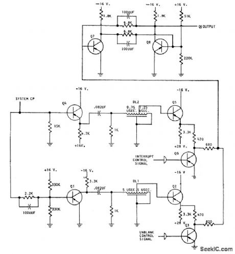

Used to interrupt or chop square wave gen orated with or in between regular system clock pulses, at specified times. Clock pulses are applied to bases of Q1 and Q4. Can be used to generate unblanking pulses without rise time deterioration, for intensifying sine and cosine waves on a radar display.-J.McGruder, Square Wave Chopper, EEE, 10:12, p26-27. (View)
View full Circuit Diagram | Comments | Reading(577)
HEX_KEBOARD_
Published:2009/7/10 22:25:00 Author:May

Circuit provides correct hexadecimal output for each key depressed, along with enable level that indicates when key has been pressed, and three switches for providing eight separate codes serving for program control. When no key is pressed, voltage at point A (lower left) and any horizontal keyboard row is 0 V and voltage on any vertical keyboard column is 5 V. When key is pressed, voltage at A becomes 1 V and voltage at selected row and column becomes 3 V. Comparator outputs for U1 and U2 are decoded with N0R gates and strobed onto data lines with open-collector NAND gates.-J. F. Czebiniak, Simple Hex Keyboard Provides Program Control, EDN Magazine, Jan. 5, 1978, p 27-28.
(View)
View full Circuit Diagram | Comments | Reading(663)
TRIGGERED_SWEEP
Published:2009/7/10 22:24:00 Author:May
Developed for use with general-purpose CR0 in troubleshooting digital circuits, to provide one horizontal sweep of cathoderay beam each time circuit is triggered by input signal pulse. Noninverting input of 741 opamp is connected to vertical amplifier of CRO,and inverting input is used to control trigger level. When input signal rises above trigger level, output of opamp swings to -V and makes output of 555 timer go high, allowing output capacitor to charge at constant cuirent through transistor in series with resistor. Resultis nearly perfect ramp voltage. All diodes are 1N914. an is any PNP switching transiston-W. J. Prudhomme, Trigger Your Oscilloscope, Kilobaud, Aug. 1977, p 34-38. (View)
View full Circuit Diagram | Comments | Reading(2041)
HIGH_Z_PROBE
Published:2009/7/10 22:24:00 Author:May
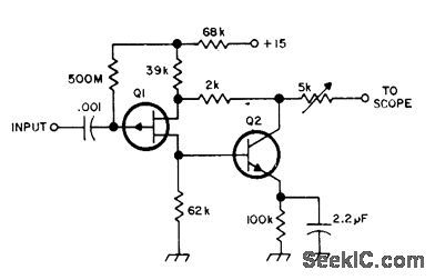
Provides about 1200-megohm input impedance to CRO, with unity gain. Pot adjusts equalization at higher frequencies. Q1 can be U112, 2N2607, 2N4360 or TIM12. Q2 can be 2N706, 2N708, 2N2926, 2N3394 or HEP 50.-Circuits, 73 Magazl'ne, March 1974, p 89. (View)
View full Circuit Diagram | Comments | Reading(1877)
CHOPPER_TYPE_REGULATOR
Published:2009/7/10 22:24:00 Author:May
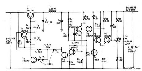
To oblain 10V at 1 amp from satellite solar cell supply with 97% effidency, differential amplifier in comparator stage produces error voltage to con trol Schmitt trigger, driver, and pctss switch.This achieves regulation by chopping current flow into filler for discrele intervals.-C. An-dren, High-Efficiency Voltage Regulator, Electronics, 37;23, p64-5. (View)
View full Circuit Diagram | Comments | Reading(880)
| Pages:202/471 At 20201202203204205206207208209210211212213214215216217218219220Under 20 |
Circuit Categories
power supply circuit
Amplifier Circuit
Basic Circuit
LED and Light Circuit
Sensor Circuit
Signal Processing
Electrical Equipment Circuit
Control Circuit
Remote Control Circuit
A/D-D/A Converter Circuit
Audio Circuit
Measuring and Test Circuit
Communication Circuit
Computer-Related Circuit
555 Circuit
Automotive Circuit
Repairing Circuit