
Index 207
TUNED_RF_WAVEMETER
Published:2009/7/10 5:40:00 Author:May
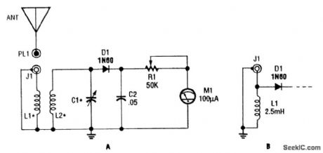
L1 and L2 form a tuned transformer. About a 1:3 turns ratio is optimum. L2 and C1 tune to the desired frequency. The frequency range can be 10 kHz to over 200 MHz, depending on the value of C1.For HP use, C1 can be a 140-pF variable. For VHF, use about 25 μF. Use of a 2.5 pH RE choke will yield an untuned wavemeter. (View)
View full Circuit Diagram | Comments | Reading(814)
LOW_SOURCE_IMPEDANCE
Published:2009/7/10 5:38:00 Author:May
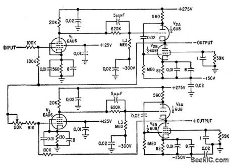
Tubes V1 and V2 provide single-phase inversion with output impedance below 0.5 ohm over 50.kc poss bond when feedback loop is dosed. Output of V2 feeds identical combination V3-V4 to provide second output in phase with input to V1. Trim adjustment is provided to insure unity gain for both outputs. Used in automatk doppler cycle counter for measuring position and velocity of missiles.-B. E. Keiser, Digital-Countor Techniques Increase Doppler Uses, Electronics, 32:21, p 46-50. (View)
View full Circuit Diagram | Comments | Reading(605)
PRECISION_CRYSTAL_FREQUENCY_CHECHER
Published:2009/7/10 5:38:00 Author:May
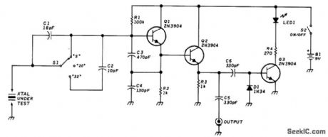
This circuit uses a Colpitts oscillator (Q1) with a buffer amplifier (Q2) to test crystals. S1 selects three load conditions-series (S), 20 pF, and 32 pF. Leads to S1 and the crystal should be kept short. The circuit should be useful over 2-to 20-MHz. (View)
View full Circuit Diagram | Comments | Reading(668)
LOW_LEVEL_1_CPS_TO_500_KC
Published:2009/7/10 5:35:00 Author:May
Features indude input impedance above 30 meg and noise figure below 3 db over wide range of generator resistantes. Bootstrapping of input stage enhances high input impedance of fet. Will operate down to 1 cps without need for large capacitors. Upper frequency limit is 500 kc for generator resistance of 100K. Voltage gain is stable within 0.5 db of 40, from -55 to +125℃.-Texas Instruments Inc., Solid-State Qommunicotions, McGraw.Hill, N.Y., 1966, p 290. (View)
View full Circuit Diagram | Comments | Reading(675)
HIGH_VOLTAGE_GAIN
Published:2009/7/10 5:33:00 Author:May
Provides gain of 3,500 into 10-meg load, by operating transistor in common-base configuration and using constant-current source in collector drcuit, Circuit is balanced, so either transistor can operctie as gain stage while other serves as current source. Feedback overcomes problem of critial d-c bias.-A. J. Adler, High-Gain Ampliner, EEE, 11:8, p 31. (View)
View full Circuit Diagram | Comments | Reading(646)
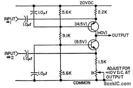
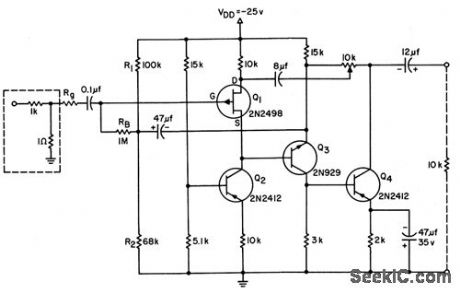
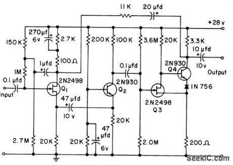
SIGNAL_VOLTAGE_STABILIZER
Published:2009/7/10 5:31:00 Author:May
Main amplifier is followed by emffier-followers to reduce fraction of d-c load current fowing in collector load of omplifier. In this conventional arrangement, overall gain is only about 500.-T. K. Hemingway, Applications of the Constant-Current Diode, Electronics, 34:42, p 60-63. (View)
View full Circuit Diagram | Comments | Reading(500)
FOUR_STATION_TWO_WAY
Published:2009/7/10 5:30:00 Author:May
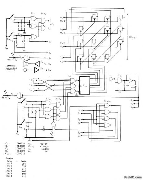
Each station can commumcate pnvately with any one of others.All four stations have identical inputs as at upper left, with fourth station having master circuit. Each two-station combination is assigned 3-bit code as given in table, for selection by switches Sw1-Sw4 All station codes are ORed and decoded by IC4 to drive matrix of analog switches for coupling appropriate audio inputs and outputs. Code 000 is used for systemfree status as indicated by LEDs 1 and 4 being on. LEDs flash for system-busy status. When code is selected, enable inputs of nonselected stations go low to prevent generation of further codes. System can be expanded to six stations by using 4-bit code and CD4514 decoder with larger matrix of analog switches.-B. Voynovich, Multiple Station Two-Way Intercom, Wireless World, March 1978, p 59. (View)
View full Circuit Diagram | Comments | Reading(876)
Light_operated_SCR_alarm_using_a_sensitive_gate_SCR
Published:2009/7/17 4:58:00 Author:Jessie
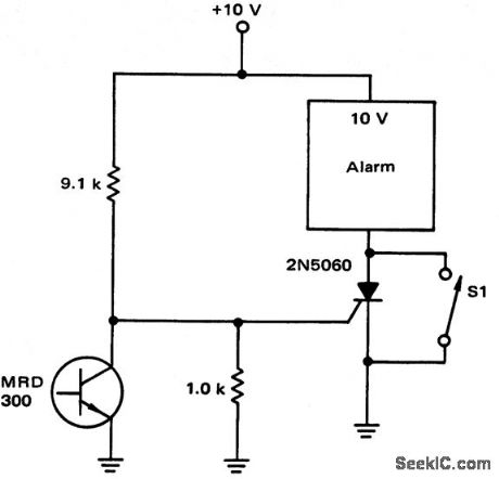
Light-operated SCR alarm using a sensitive gate SCR (courtesy Motorola Semiconductor Products Inc.). (View)
View full Circuit Diagram | Comments | Reading(1064)
DOUBLE_BOOTSTRAPPED_FET
Published:2009/7/10 5:26:00 Author:May
Both drain and source are bootstrapped in 6-db high-input-impedance amplifier, to reduce effect of fet capacitances so they are insignificant compared to stray circuit capacitances at input terminal. 10-K pot provides gain compensation adiustment.-L. J. Sevin, Jr., Field-Effect Transistors, McGraw-Hill, N.Y., 1965, p 69. (View)
View full Circuit Diagram | Comments | Reading(595)
FLIP_FLOP_INDEPENDENT_LAMP_DRIVER
Published:2009/7/10 5:25:00 Author:May
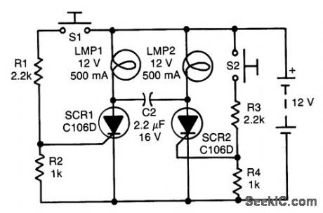
Assume first that SCRt is on and SCR2 is off so that C1 is fully charged, with its LMP2 end positive. The state of the circuit can be changed by pressing S2. As SCR2 turns on, it turns SCR1 off capacitively via its anode. Capacitor C1 then recharges in the opposite manner (i.e., the left end is now positive). The state of the circuit can be changed again by pressing S1, thus driving SCR1 on by way of its gate, and driving SCR2 off capacitively via its anode. (View)
View full Circuit Diagram | Comments | Reading(665)
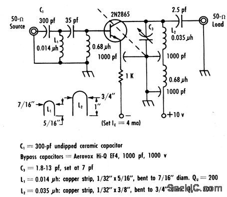
UHFSOURCEDIPPER
Published:2009/7/10 5:24:00 Author:May
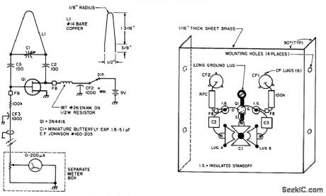
This dipper is useful for UHF experiments in the 420-to-450 MHz amateur band. Because layout can affect performance, follow Fig. 48-2(b) (View)
View full Circuit Diagram | Comments | Reading(773)
100_MC_CASCADED
Published:2009/7/10 5:23:00 Author:May
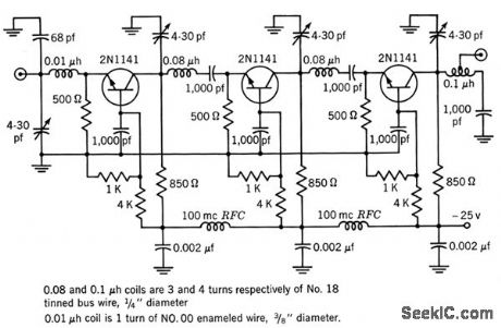
Uses mismatch design technique to obtain desired overall gain of 37.5 db at bandwidth of 9 Mc for three cascaded stages.-Texas Instruments Inc., Transistor Circuit Design, McGraw-Hill, N.Y.,1963,p 290. (View)
View full Circuit Diagram | Comments | Reading(664)
250_MC_R_F_FOR_MILITARY_VHF_BAND
Published:2009/7/10 5:22:00 Author:May
Gives 12.5 db gain and noise figure of only 5 db, with excellent stability.-Texas Instruments Inc., solid-State Communications, McGraw-Hill,N.Y.,1966,p 297. (View)
View full Circuit Diagram | Comments | Reading(651)
WIDEBAND_UNITY_GAIN_FET
Published:2009/7/10 5:21:00 Author:May
Input impedance is about 100 meg, and response is within 3 db from below 10 cps to 1 Mc for 100K generator resistance.-Texas Instruments Inc., Solid-State Communications, MAcGraw-Hill, N.Y., 1966, p 296. (View)
View full Circuit Diagram | Comments | Reading(752)
30_MC_DOUBLE_TUNED
Published:2009/7/10 5:19:00 Author:May
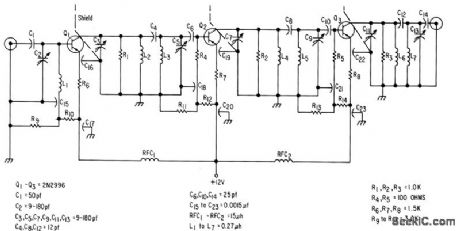
Proper loading provides good stabilily along with gain of 21 db per stage,despite inherent instability of 2N2996 at this frequency. Total power gain is thus 63 db, for noise figure of 2.3 db and bandwidth of 3 Mc.-Texas Instruments Inc., solid-Stale Communications, McGraw-Hill,N.Y, 1966, p 310. (View)
View full Circuit Diagram | Comments | Reading(582)
DIVIDE_BY_N_1_2_CIRCUIT
Published:2009/7/10 5:18:00 Author:May
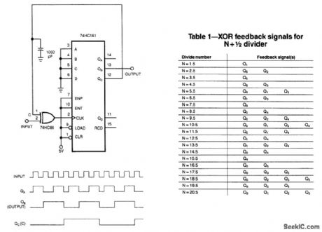
This circuit, instead of dividing by an integer, divides the input signal by N+1/2. With the feedback connections exactly as the figure shows, the circuit divides by 3.5. Point C ultimately controls when the input clocks the 74HC1614-bit counter. When C=0, the positive edge of the input triggers the counter. If C=1, the negative edge of the input triggers the counter. Each time that point C changes level, the circuit shortens the output pulse width of the counter by half of an input cycle. Thus, the counter's divisor depends on how many changes occur at point C during one output period.
Although the figure divides by 3.5, feeding back different counter outputs produces different divisors. Generally, an m-bit binary counter with pure exclusive-OR (XOR) feedback can form an N+1/2 counter, where N ranges from 2m-2+1/2 to 2m-1/2. The divided output is available at the m-1 bit of the counter. (View)
View full Circuit Diagram | Comments | Reading(1131)
A_C_COUPLED_CASCODE
Published:2009/7/10 5:18:00 Author:May
Circuit is uniquely suited to inerectsing bandwidth of low-noise amplifier by reducing miller effect and per mining independent adiustment of operating conditions for optimum noise performance,-Texas Instruments Inc., Solid-Stale Communications, Mc Graw-Hill, N.Y.1966, p 143. (View)
View full Circuit Diagram | Comments | Reading(603)
AF_OUTPUT
Published:2009/7/10 5:17:00 Author:May
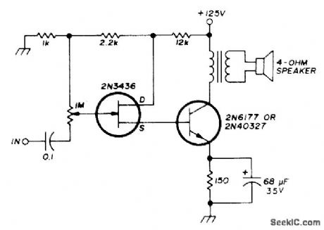
Operates directly from 125-V rectified AC line voltage. Combination of unipolar and bipolar transistors gives desirable amplifying features of each solid-state device.-I. M.Gottlieb, A New Look at Solid-State Amplifiers, Ham Radio, Feb. 1976 p 16-19. (View)
View full Circuit Diagram | Comments | Reading(981)
OP_AMP_POWER_DRIVER
Published:2009/7/10 5:13:00 Author:May
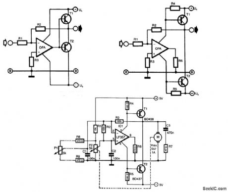
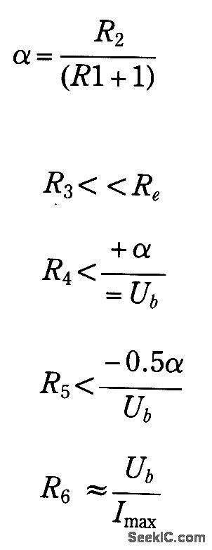
Frequently, the output current of an operational amplifier is inadequate for the application as, for instance, when a small motor or loudspeaker has to be driven. Normally, this is resolved by adding an emitter follower to the circuit as shown in Fig. 27-1(a). Unfortunately, that circuit does not allow the full supply voltage, Ub, to be used, because the output voltage of the op amp must always be 1 to 2 V smaller than ± Ub. To that must be added the drop across the base-emitter junction of transistors T1 and T2.
The circuit shown in Fig. 27-1(b) (principle) and Fig. 27-1(c) (practical) is a more appropriate solu-tion: it was designed specifically for driving small motors. Since the output current of the op amp flows through its supply lines, the driver transistors may also be controlled over these lines.
The value of base-emitter resistors R4 and R5 has been chosen to ensure that in spite or the quiescent current through the op amp, T1 and T2 are switched off. Resistor R6 limits the output current of the op amp. If the op amp is a type with guaranteed short-circuit protection, R6 may be replaced by a jump lead.
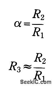
The output voltage is only 50 to 100 mV (collector-emitter saturation voltage of the driver transistors) smaller than the supply voltage. When choosing these transistors, it is therefore essential to take into account the saturation voltage (in addition to the maximum current amplification and power rating).The value of the resistors in an Inverting circuit is calculated from:
where α is the amplification.
In a noninverting circuit (R1 between the -input and ground and the input signal connected to the +input of the op amp), the amplification is:
where Re is the input impedance of the op amps.
The circuit can be used with discrete (single) op amps only, because double or quadruple types in one package share the supply voltage pins. The setting accuracy of the circuit in Fig. 27-1(c) is better than 1%. (View)
View full Circuit Diagram | Comments | Reading(910)
1_W_AT_6_V_
Published:2009/7/10 5:08:00 Author:May
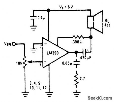
Battery-operated power amplifier using National LM390 IC provides ample power for loudspeaker despite operation from 6-V portable battery.- Audio Handbook, National Semiconductor, Santa Clara, CA, 1977, p 4-41. (View)
View full Circuit Diagram | Comments | Reading(679)
| Pages:207/471 At 20201202203204205206207208209210211212213214215216217218219220Under 20 |
Circuit Categories
power supply circuit
Amplifier Circuit
Basic Circuit
LED and Light Circuit
Sensor Circuit
Signal Processing
Electrical Equipment Circuit
Control Circuit
Remote Control Circuit
A/D-D/A Converter Circuit
Audio Circuit
Measuring and Test Circuit
Communication Circuit
Computer-Related Circuit
555 Circuit
Automotive Circuit
Repairing Circuit