
Index 219
BIT_GRABBER
Published:2009/7/9 23:03:00 Author:May
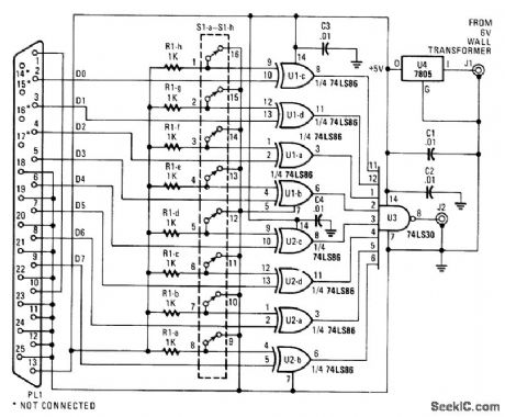
When the user set character (D0 through D7) from a computer matches the character programmed on SIA through S1A, the output from J2 becomes low. This device can be used as a test aid to check printer cable or as a control circuit for interfacing with a computer. (View)
View full Circuit Diagram | Comments | Reading(651)
FACSIMILE_SYNC_PULSE_SHAPER
Published:2009/7/20 1:54:00 Author:Jessie
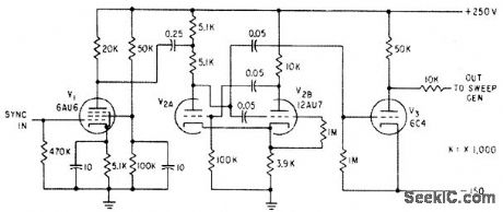
Used to change shape of high-precision sync pulse for facsimile recorder in order to change time of return trace. Amplifier V1 is coupled to plate driven one-shot mvbr whose time constants determine return trace time.-E. W. Winkle, High-Precision Sweep Generator, return trace. Amplifier V1 is coupled to plate. Electronics, 33:50, p 88-90. (View)
View full Circuit Diagram | Comments | Reading(558)
RS_232C_LINE_DRIVEN_CMOS_CIRCUITS
Published:2009/7/9 23:02:00 Author:May
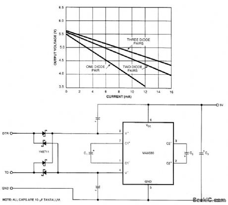
The circuit illustrates a way to power CMOS ICs from RS-232C lines. The MAX680 is normally used to generate a voltage eqqal to ±2 x VCC. This circuit does exactly the opposite. It takes in t 10.5 to ±12 V on the DTR and TD lines and puts out a 5.25- to 6-V signal. A pair of Schottky or silicon diodes rectifies each RS-232C line. The resultant energy is stored by the capacitors attached to the IC's V+ and V - pins. C1 or both C1 and C2 then reverse-charge pump the energy stored at the V+ and V- pins to C3. The input source current of the MAX680 is approximately equal to the voltage drop of any one of the diodes that is divided by the series resistance of 160Ω. When you drive this circuit from a 1488 driver with a ±12-V supply, it can deliver 5 V at 3 mA.
To increase the output current, you can use as many as three sets of diodes on each RS-242 line to provide 5 V at 8 mA. The more diodes you use, the lower the source resistance: RS equals the inversion of the sum of the diodes' conductances. If your circuit requires even more output current, you can place two MAX680s in parallel, tie their V + and V- capacitors together, and use separate C1 and C2 capacitors for each ship. If you do connect the devices in parallel, make sure not to exceed the power capability of the RS-232C lines. (View)
View full Circuit Diagram | Comments | Reading(750)
ANALOG_VOLTAGE_COMPARATOR
Published:2009/7/20 1:52:00 Author:Jessie
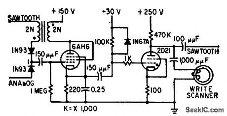
When sawtooth amplitude exceeds analog voltage, positive feedback loop of blocking oscillator is completed through conducting diode and oscillator conducts, triggering thyratron writing circuit for magnetic drum.-H. L. Daniels and D. K. Sampson, Magnetic Drum Provides Analog Time Delay, Electronics, 32:6, p 44-47. (View)
View full Circuit Diagram | Comments | Reading(929)
Z_80_BUS_MONITOR_DEBUGGER
Published:2009/7/9 22:57:00 Author:May
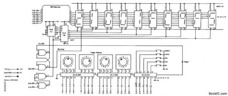
Getting microprocessor designs to work is notoriously difficult when both the software and hardware are new. The usual approach is to run test routines that address memory and I/0, but do not rely on their correct functioning. However, miswiring in any part of the circuit usually leads to a misleading jumble of signals that might require a logic analyzer to interpret.
This simple circuit will trace the program execution and help point to the problems. Although the circuit shows connections for a Z-80, the circuit can very easily be adapted for any 8-bit microprocessor or with additional circuitry for CPUs of any bus width.
The circuit consists of a 5-byte hexadecimal display and comparator, which are wired to a 40-pin IC test clip. The test clip sits over the microprocessor (in this case a Z-80), where it gets power and all the required signals. The address bus and control lines are fed to the comparator, where (by means of switches) a trigger condition can be set. Following the trigger, the next 5 occurrences of either RD or WR will latch the contents of the data bus into the 5 hex displays, each in turn.
For example, select address 0000 M1 Rd and reset the CPU. The displays will show the very first instruction fetch, followed by its data and any consequent action. Even details, such as stack writes and subroutine addresses, are included. lb trace longer por-tions of a program the address switches can be incremented to follow the execution path. (View)
View full Circuit Diagram | Comments | Reading(717)
BEEPER_FOR_TELEPHONE_RECORDING
Published:2009/7/20 1:49:00 Author:Jessie
Generates periodic 1,400-cps tone or beep having 0.2 sec duration, at intervals of about 15 sec, as required by Federal law when recording or broadcasting telephone conversations.-J. Zelle, Phone Calls for Broad-cast, Electronics, 31:45, p 96-101. (View)
View full Circuit Diagram | Comments | Reading(649)
AUTOMATIC_EMERGENCY_LIGHTING_UNIT
Published:2009/7/9 22:53:00 Author:May
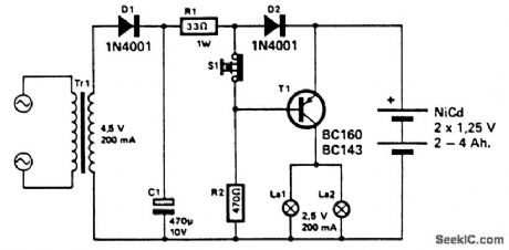
This unit uses a Nicad battery to provide power to an emergency lighting setup. When power fails, T1 becomes forward biased, which lights L1 and L2. The batteries are normally kept charged. When power is on, T1 is cut off and it keeps the lamps extinguished. (View)
View full Circuit Diagram | Comments | Reading(977)
LIGHT_DIMMER
Published:2009/7/9 22:51:00 Author:May
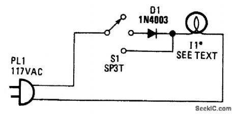
Lamp I1 is a household lamp. When the switch is in the center position, the lamp is operated on half-wave rectified ac; the effective voltage the lamp sees is less, which dims it. I1 can be a lamp up to 200 W or 50 rated at 120 or 240 V, and D1 should be a 200-V PlV or better diode (400PIV for 240-V operation). (View)
View full Circuit Diagram | Comments | Reading(667)
HIGH_IMPEDANCE_DIFFERENTIAL_INPUT
Published:2009/7/9 22:48:00 Author:May
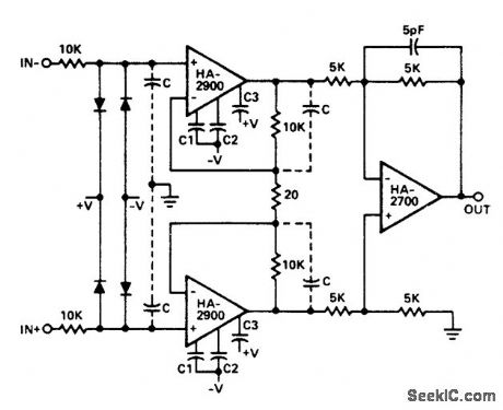
Two Harris HA-2900 chopper-stabilized opamps feed HA-2700 high-performance opamp for instrumentation applications. Circuit provides excellent rejection of ±10 V common-mode input signals. Protection diodes prevent voltages at input terminals from exceeding either power supply. Supply can be ±15 V.- Linear & Data Acquisition Products, Harris Semiconductor, Melbourne, FL, Vol. 1, 1977, p 7-70 (Application Note518). (View)
View full Circuit Diagram | Comments | Reading(768)
LINEAR_OHMMETER
Published:2009/7/9 22:44:00 Author:May
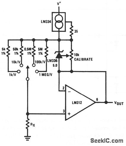
View full Circuit Diagram | Comments | Reading(1967)
002_WEIGHING_ACCURACY
Published:2009/7/9 22:43:00 Author:May
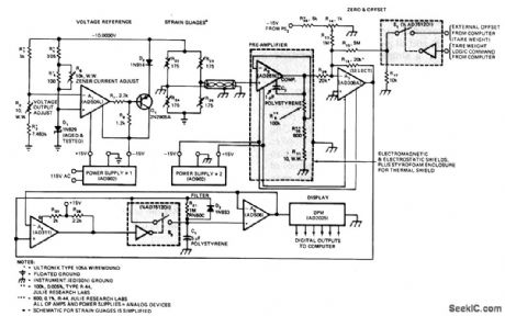
Analog instrument covers up to 300 lb with resolution of 0.01 lb, for monitoring changes in body weight during clinical study. Bonded strain gages distributed symmetrically on platform of scale form bridge network R1-R2-R4-R5 serving as input for circuit that displays weight on digital panel meter and provides digital outputs to computer. Proper grounding is critical; all ground returns should go to single point at each powersupply common line. Article covers circuit operation in detain-J. Williams, This 30-PPM Scale Proves That Analog Designs Aren't Dead Yet, EDN Magazine, Oct. 5, 1976, p 61-64. (View)
View full Circuit Diagram | Comments | Reading(888)
DUAL_8051s_EXECUTE_IN_LOCK_STEP
Published:2009/7/9 22:43:00 Author:May

This hardware-software combination deletes clocks from the slave μP until both μPs synchronize. The firmware loop causes each μP to generate a WR signal once per loop. The circuit exclusive-0Rs the two WR signals to produce a miss-compare pulse. The miss-compare pulse latches into the two JK flip-flops via outputs LOCKSTP1 and LOCKSTP2. A high on these signals indicates that the μPs are in lock-step, causing both μPs' programs' execution to exit the firmware loop. If you use discrete components, you'll probably want to use the 0 output of the JK flip-flop and delete the circuit's inverters.
The listing uses the μPs' ports 1 and 3. You cannot use a memory-mapped location for the lock-stepdetect clear (K input) because this scheme would generate additional WR signals. You could apply this idea to other μPs, perhaps using their RD signals. This way, generating an RD signal to activate the lock-step-detect clear would not affect the synchronization inputs. (View)
View full Circuit Diagram | Comments | Reading(579)
Composite_AM_FM_IF_amplifier_and_detector_circuitry
Published:2009/7/20 2:57:00 Author:Jessie
Composite AM/FM IF amplifier and detector circuitry (courtesy Motorola Semiconductor Products Inc.). (View)
View full Circuit Diagram | Comments | Reading(694)
146_MHz_RECEIVER_PREAMP
Published:2009/7/20 2:56:00 Author:Jessie
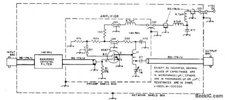
Uses 146-MHz bandpass crystal filter to suppress front-end in-termodulation-distortion products (IMD) in VHF repeater circuits while providing gain of 6-8 dB to overcome filter insertion loss. Also helps front-end overload problems from strong adjacent-channel amateur signals. Filter response is down 40 dB at ±38 kHz and down over 50 dB beyond 60 kHz from filter center frequency. Filter used is Piezo Technology TM-4133VBP.Input and output for filter should be exactly 50 ohms.-J. M. Hood, Monolithic Crystal Filter Application in Amateur VHF Repeaters, QST, July 1975, p 27-29 and 48. (View)
View full Circuit Diagram | Comments | Reading(2218)
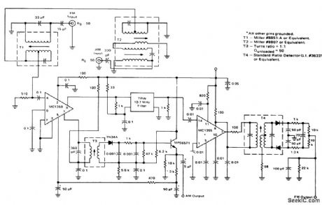
FM_IF_amplifier_detector_and_audio_amplifier_with_1_watt_output
Published:2009/7/20 2:55:00 Author:Jessie
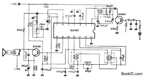
FM IF amplifier detector and audio amplifier with 1-watt output. The ECG1057 is a 14-pin DIP. The circuit shown can be adapted for either 4.5 MHz or 10.7 MHz. Select the IF transformers accordingly. Coils and transformers are standard and can be purchased at Radio Shack (courtesy GTE Sylvania Incorporated). (View)
View full Circuit Diagram | Comments | Reading(1133)
100_Hz
Published:2009/7/20 2:54:00 Author:Jessie

Simple and stable subaudible tone generator serves for access to FM repeaters.Frequency is adjusted to that of repeater with 20K pot. Will operate from car battery.-Circuits, 73 Magazine, Sept. 1973, p 143. (View)
View full Circuit Diagram | Comments | Reading(1116)
CONTROL_FUNCTION_DECODER
Published:2009/7/20 3:07:00 Author:Jessie
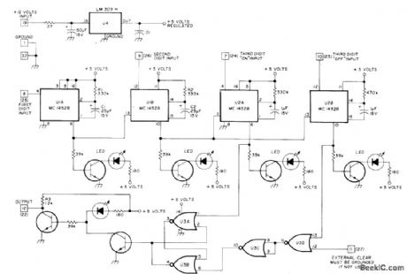
Circuit detects predetermined 3-digit sequence of Touch-Tone signals and sets flip-flop to provide required output for activating desired function.Another 3-digit sequence, differing in only third digit, resets flip-flop for turning off controlled device. Circuit uses two dual mono MVBRs. Output of U1A goes to reset terminal of U1B.Output of U1B goes to reset terminals of monos U2A and U2B. Mono outputs drive RS flip-flop to provide output required for desired control fu notion, such as control of autopath, switching repeater mode from carrier to tone-access, and switching to remote receiver. Q1-Q6 can be almost any NPN silicon transistors, such as 2N3904. U3 can be MC14001 or CD4001. Numbers in boxes and parentheses refer to edge connector pins.-T. E. Doyle, Control Function Decoder, Ham Radio, March 1977, p 66-67. (View)
View full Circuit Diagram | Comments | Reading(932)
DELAYED_VOX
Published:2009/7/20 3:06:00 Author:Jessie
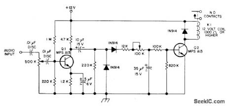
Minimizes unintentional triggering of repeater by using timer requiring 3 s of continuous carrier and audio on input receiver of repeater to turn on transmitter. Repeater is then controlled by its own carrier-operated relay until 20-s lapse in transmission occurs. System then requires another3-s carrier to restore normal operation, Q1 is common-emitter amplifier with gain adjusted by 500K pot. Audio peaks from al feed full-wave diode detector through 10-ptF electrolytic. Series resistance in path through 35-ptF electrolytic controls its charge-up time and thus controls delay of relay pickup. Adjust 100K pot to give desired turn-on delay in range from fraction of second to about 4 s. Resistance divider shown provides relay dropout delay of about 20 s, which pre-vents VOX circuit from dropping out repeater during lapses in speech.-J. Everhart, A Delayed VOX for Repeaters, 73 Magazine, April 1974, p 17 and 19-20. (View)
View full Circuit Diagram | Comments | Reading(5298)
107_MHz_FM_IF_amplifier_with_detector
Published:2009/7/20 3:04:00 Author:Jessie
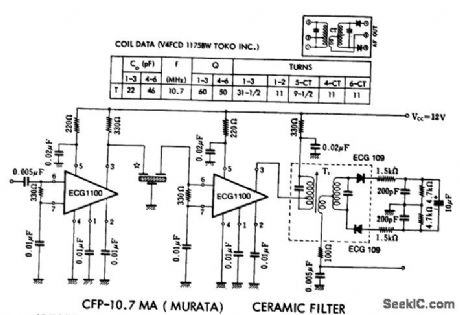
10.7 MHz FM IF amplifier with detector.coil data for the transformer is shown in the table,The ECG1100 is a 7-pin module,Typical voltage gain per unit is 56 dB,Total supply current for the entire circuit is 21 mA.The detector output for a 60 dB Input is go mV(courtesy GTE Sylvania Incorporated). (View)
View full Circuit Diagram | Comments | Reading(3697)
TONE_BURST_FOR_MIKE
Published:2009/7/20 3:04:00 Author:Jessie
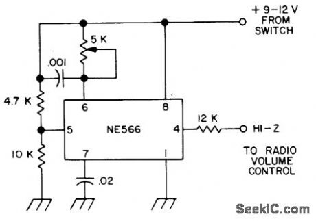
Uses NE566 PLL function generator to provide tone entry into 2-meter repeaters. Output is fed into volume control of any AM transistor radio, and loudspeaker is held in front of transceiver microphone when tone is desired.-F. J. Derfler, An Acoustically Coupled Digital Keyed Squeaker for Tone Burst Entry, 73Magazine, Aug, 1973, p 27-30. (View)
View full Circuit Diagram | Comments | Reading(764)
| Pages:219/471 At 20201202203204205206207208209210211212213214215216217218219220Under 20 |
Circuit Categories
power supply circuit
Amplifier Circuit
Basic Circuit
LED and Light Circuit
Sensor Circuit
Signal Processing
Electrical Equipment Circuit
Control Circuit
Remote Control Circuit
A/D-D/A Converter Circuit
Audio Circuit
Measuring and Test Circuit
Communication Circuit
Computer-Related Circuit
555 Circuit
Automotive Circuit
Repairing Circuit